#HighFrequencyPCB
Explore tagged Tumblr posts
Visit Tumblr Blog
Explore Tumblr blogs with no restrictions, modern design and the best experience.
Last Seen Tumblr Blogs


Fun Fact
12.7% of mobile users access Tumblr.
Text
#SolderMask#PCBDesign#ElectronicsEngineering#CircuitBoard#PCBManufacturing#LaserDirectImaging#UVSolderMask#EcoFriendlyTech#IPCStandards#HighFrequencyPCB#HalogenFree#TechnologyAdvancements#SustainableManufacturing#ElectronicComponents#EngineeringInnovation#USA#Europe#switzerland#germany
0 notes
Text
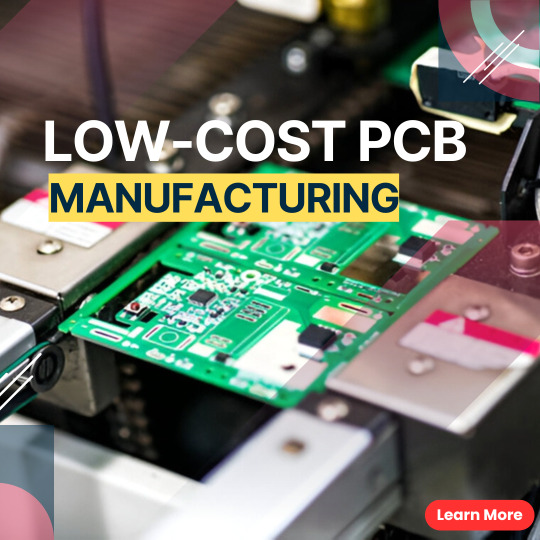
📡 High-Frequency PCB Manufacturing Techniques 🔧
High-frequency PCBs are crucial for advanced communication and RF applications. Here's a breakdown of their manufacturing techniques:
🔍 Key Highlights: ✔️ Material Selection: Use specialized substrates like PTFE, Rogers, or ceramic for minimal signal loss and high stability. ✔️ Precision Etching: Ensures accurate trace dimensions to maintain impedance control. ✔️ Multilayer Design: Essential for complex circuits to support high-speed signal integrity. ✔️ Plating Techniques: Employ advanced methods like ENIG (Electroless Nickel Immersion Gold) for reliable connections. ✔️ Testing Protocols: Rigorous testing for dielectric constant (Dk) and dissipation factor (Df) to ensure performance.
Pro Tip: Focus on low-loss materials and precise manufacturing to enhance signal quality and reduce interference. 🚀
���� Learn more: https://www.viasion.com/blog/low-cost-pcb-manufacturing/
0 notes
Text
Printed Circuit Board Manufacturers
Introduction
In today's technological landscape, printed circuit boards (PCBs) are at the heart of countless electronic devices. Whether it's smartphones, computers, or medical equipment, PCBs play a critical role in connecting and powering various components. When it comes to choosing a PCB manufacturer, it's essential to find a reliable partner that can meet your specific requirements. In this article, we will explore the top 4 PCB manufacturers in the USA, highlighting their strengths and capabilities.
What is a PCB?
Before diving into the details, let's briefly understand what a PCB is. A printed circuit board is a flat board made of non-conductive material, usually fiberglass, with copper tracks etched or printed onto it. These tracks serve as electrical pathways, connecting different electronic components such as resistors, capacitors, and integrated circuits. PCBs provide mechanical support and facilitate the efficient flow of electrical signals, making them vital in modern electronic devices.
Importance of choosing the right PCB manufacturer
Choosing the right PCB manufacturer is crucial for the success of any electronic product. The quality, reliability, and performance of the PCB can significantly impact the overall functionality and longevity of the device. A reputable manufacturer ensures that the PCBs are manufactured to meet industry standards, undergo thorough testing, and are built to withstand various environmental conditions.
Factors to consider when choosing a PCB manufacturer
When selecting a PCB manufacturer, several factors should be taken into consideration:
Quality and reliability: Look for manufacturers with a track record of producing high-quality and reliable PCBs. Quality control measures, certifications, and adherence to industry standards are indicators of a manufacturer's commitment to excellence.
Manufacturing capabilities: Assess the manufacturer's manufacturing capabilities, including equipment, production capacity, and technological expertise. This ensures they can handle your specific project requirements effectively.
Technical support and customer service: Good technical support and responsive customer service are invaluable when it comes to resolving any issues or addressing concerns throughout the PCB manufacturing process.
Pricing and lead times: Evaluate the manufacturer's pricing structure and lead times to ensure they align with your project budget and timeline. Balancing cost-effectiveness with timely delivery is crucial.
Visit for more information on PCB Manufacturers: https://www.acmecircuit.com/blog/
#PCBManufacturers#PCBManufacturing#PrintedCircuitBoard#CircuitBoardAssembly#CircuitBoardManufacturing#PCBBoardManufacturer#HighFrequencyPCB#PCBManufacturersNearMe#PCBManufacturer#PCBSupplier#PCBAssemblyServices#PCBAssemblyManufacturer#ElectronicCableAssembly#ElectronicContractServices#PCBExporters#PrintedCircuitBoardManufacturer#PCBManufacturingCompanies#PCBManufacturerIndia#PCBIndustry#PCBSolutions#ElectronicManufacturing#PCBPrototyping#PCBDesign#ElectronicsProduction#PCBQualityControl#ElectronicsEngineering#PCBTechnology#PCBExperts#PCBInnovation#PCBManufacturingProcess
0 notes
Text
High Speed PCB Design
Maintaining high speed PCB design quality from the driver to the collector on the PCB is not an easy task. One of the most testing issues is dealing with the engendering deferral and relative time postpones bungles. To deal with the time delays, we have to realize how to figure follow length from time postpone an incentive to execute the PCB support steering as needs are. Let me show you the procedure. The high-frequency PCB design also requires selective material for PCB.
Finding a high Speed PCB Design
As per material science, swift sign travels in a vacuum or through the air at a similar speed As light, which is. Looking for high speed PCB design: According to materials science, electromagnetic signals travel in a vacuum or in the air at a speed similar to that of light, that is: Vc = 3 x 10⁸ m/s = 186,000 miles/s = 11.8 inches/ns Due to the influence of the dielectric constant (Er) of the PCB material, the signal passes through the PCB transmission line at a slower speed. In addition, the transmission line structure also affects signal speed.
There are two general PCB follow structures:
stripline
microstrip
The equations for computing the sign speed on a high-frequency PCB are given underneath:
Where:
Vc is the speed of light in a vacuum or through the air
Er is the dielectric steady of the PCB material
Ereffis the compelling dielectric consistent for microstrips; it’s worth lies among one and Er, and is roughly given by:
Ereff≈ (0.64 Er+ 0.36) (1c)
Figuring engendering delay (TPD)
The spread deferral is the time a sign takes to increase over a unit length of the transmission line.
Here is how we determine the diffusion delay from the following lengths and other methods: Where: symbol speed relative to the transmission line In a vacuum or air, it rises to 85 picoseconds per inch (ps/ In).
On PCB transmission lines, the engendering delay is given by:
How to choose High-Speed PCB Design Material
Before selecting the high-speed PCB material for your fast PCB plan, it is essential to decide a worth (or qualities) for DK and Z0 for your transmission line (or lines). Your high-speed PCB board structure programming may enable you to set these qualities and incorporate them as a component of the plan file(s) for your agreement maker (CM). If not, there are dk outlines and impedance mini-computers online to assist you with landing at the best possible qualities. Presently, you are prepared to actualize the 2-advance answer for your fast PCB structure material choices!
Stage 1: Select board material sorts
Pick material sort from types prescribed for high-recurrence PCBs. This incorporates choosing center, prepreg, and substrate materials. You might have the option to profit by half breed development, where sign layer material is picked for high recurrence. Yet, different layers may utilize different materials to diminish manufacturers’ costs.
Stage 2: Select board material thicknesses and copper loads
Utilize your determined or favored qualities for DK and Z0 to choose thickness and copper loads. Make sure to keep up impedance consistency all through sign ways. Your CM ought to be a piece of your material choice procedure as the board manufacture, and PCB gets together stages may expect adjustments to your determinations before your sheets can be made. Rhythm Automation, the industry head in quick, exact PCB model assembling, is prepared to band together with you and help you in upgrading the material determination process.
Also, to assist you with beginning on the best way, we outfit data for your DFM and empower you to see and download DRC documents effectively. In case you’re an Altium client, you can permanently add these documents to your PCB structure programming.
If you are prepared to have your plan made, attempt our statement device to transfer your CAD and BOM documents. If you need more data on rapid PCB plan or making material determinations for your board, get in touch with us.
Impedance Matching in High-Speed PCB Design
It isn’t predominantly to take a gander at the recurrence, yet the key is to take a gander at the steepness of the edge of the sign, that is, the ascent/fall time of the sign. It is commonly viewed as that if the ascent/fall time of the sign (in 10% to 90%) is under multiple times the wire delay, it is fast. The sign must focus on the issue of impedance coordinating. The wire delay is ordinarily 150ps/inch.
Standard Impedance Matching Method
1. Couple Terminal Matching:
Under the condition that the sign source impedance is lower than the trademark impedance of the transmission line, a resistor R is associated in arrangement between the source end of the sign and the transmission line, so the yield impedance of the source end coordinates the trademark impedance of the transmission line, and the sign reflected from the heap end is stifled. Re-reflection happened.
2. Parallel Terminal Matching:
For the situation where the impedance of the sign source is little, the info impedance of the heap end is coordinated with the trademark impedance of the transmission line by expanding the parallel obstruction, to wipe out the reflection at the heap end. The execution structure is isolated into two
Coordinating obstruction choice guideline: For the situation of a high information impedance of the chip, for a solitary opposition structure, the parallel opposition estimation of the heap terminal must be near or equivalent to the trademark impedance of the transmission line; for the double obstruction structure, each parallel obstruction esteem It is double the trademark impedance of the transmission line.
The benefit of parallel end coordinating is primary and straightforward. The notable drawback is that it will bring DC control utilization: the DC control utilization of the single obstruction mode is firmly identified with the obligation cycle of the sign; the binary opposition mode is whether the symptom is high or low. There is DC control utilization; however, the current is not precisely 50% of the single resistor. Moreover, high-speed PCB design guidelines are enough to guide you.
0 notes
Photo


High frequency PCB,used Rogers Duroid/Rt 5880 material,with er(DK)=2.2, thickness 0.8mm,4 days finished before the Chinese New Year holiday , will freight to overseas by DHL.
1 note
·
View note
Link

#circuit board manufacturing#HighFrequencyPCB#AdvancedCircuitsPCB#RigidPrintedCircuitBoards#BlindViasPCB#PCBManufacturing
0 notes
Photo

Printed Circuit Board Manufacturer That You Can Trust On Agile Circuit www.agipcb.com #PCBManufacturingChina #HighFrequencyPCB #AdvancedCircuitsPCB #PCBManufacturing [email protected] https://www.instagram.com/p/Bp6Y9DzH3W7/?utm_source=ig_tumblr_share&igshid=1rwmsd18cc0l5
0 notes
Text
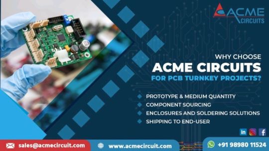
Top PCB Manufacturers In India

https://www.acmecircuit.com Are providers of top quality printed circuit board suppliers, printed circuit board manufacturers & rigid boards suppliers, etc at the industrial level at reasonable rates. For more info please contact us at (+91 98980 11524)
#PCBManufacturers#PCBManufacturing#PrintedCircuitBoard#CircuitBoardAssembly#CircuitBoardManufacturing#PCBBoardManufacturer#HighFrequencyPCB#PCBManufacturersNearMe#PCBManufacturer#PCBSupplier#PCBAssemblyServices#PCBAssemblyManufacturer#ElectronicCableAssembly#ElectronicContractServices#PCBExporters#PrintedCircuitBoardManufacturer#PCBManufacturingCompanies#PCBManufacturerIndia#PCBIndustry#PCBSolutions#ElectronicManufacturing#PCBPrototyping#PCBDesign#ElectronicsProduction#PCBQualityControl#ElectronicsEngineering#PCBTechnology#PCBExperts#PCBInnovation#PCBManufacturingProcess
1 note
·
View note
Text
Material Selection for High frequency PCB
High Frequency Printed Circuit Board is a class of PCBs. These are mostly used in those applications which involve special signal transmissions. These mostly operate in the frequency range of 500 MHz to 2GHz. High frequency PCB is a viable choice for applications involving microwave, mobile, and radio frequency.
Most of the electronic products today involve signal communication. This is more prominent in products that involve satellite and Wi-Fi systems. So, we look towards high frequency boards whenever we need a signal communication in our electronic products.
Today we will discuss all high frequency PCB boards and how you can use them as per your needs and requirements.
Material Selection for High frequency PCB Fabrication
We mostly use high frequency laminates in high frequency PCB. However, these are often difficult to fabricate. Because they must maintain the thermal heat transfer of the application due to the sensitivity of the transmitted signal. So, we need special materials for high frequency PCB manufacturing.
When you are selecting a material for High frequency PCB, you must keep the following in mind,
Dielectric constant
It is the ability of a material to store energy when we apply an electric field. However, it is a directional property which means that it will change with the axis of the material. So, the material you intend to use should have a small dielectric constant. Therefore, it will deliver stable input and there will be no delay in the transmission signal.
Dissipation Factor
Your material should also have a small dissipation factor. Because a high dissipation factor can affect the quality of the transmitted signal. However, a small dissipation factor will allow for less signal wastage.
Loss Tangent
It depends on the molecular structure of the material and it can affect the RF material going through high frequencies.
Proper spacing
It is important in terms of skin effect and cross talk. Crosstalk takes place when the PCB starts interacting with itself and we observe undesired coupling between the components. So, we need to ensure the minimum distance between the plane and trace in order to avoid crosstalk. The skin effect is related to the resistance of the trace. However, skin effect becomes prominent as the resistance increases. So, this can lead to warming the board. Therefore, the trace length and width must be such that it can’t affect the PCB at high frequencies.
The diameter of the VIA
VIAs with smaller diameters have low conductance hence, they are more suited when we are dealing with high frequencies.
Coefficient of thermal expansion
It determines the impact of temperature on the size of the material. So, this becomes important during the assembly and drilling processes. Because even a slight change in the temperature can significantly alter the size of the material. So, you must ensure that the thermal expansion of the foil must be the same as that of the substrate. Otherwise, the foil might dissociate when we subject it to high temperatures.
So, based on these considerations, we recommend the following materials for high frequency PCB,
Taconic RF-35 Ceramic
Rogers RO3001
Taconic TLX
Rogers RO3003
ISOLA IS620 E-fiber glass
Rogers 4350B HF
ARLON 85N
Features of High frequency PCB
High frequency PCB is supposed to give excellent performance. So, they have the following typical features.

Benefits of High frequency PCB
High frequency PCB service is a convenient choice when it comes to wiring. Because they shorten the connection between the various electronic components and hence, they shorten the length of the wiring. So, this consequently improves the speed of signal transmission.
High frequency PCB allows the signal line to form a constant low impedance to the ground. So, this significantly reduces the circuit impedance and provides an improved shielding effect.
Most electronic products have functional requirements of heat dissipation and high frequency PCB are made from such material that facilitates heat dissipation hence, they are an ideal fit.
The PCBs which we use in telecommunication or high-speed products are subjected to high frequencies. So, ordinary PCBs can’t function at these frequencies that is why we need high frequency PCB.
Applications of High frequency PCB
High frequency PCB has a range of applications and we will take a look at some of them,
Medical Applications
We can use high frequency PCB in healthcare or personal monitors such as heart rate monitors, blood glucose monitors, and blood pressure monitors.
You can also use them in medical scanners such as CT scanners, X-Ray scanners, and MRI scanners.
Also, we can also use them in photometers and microscopes.
Industrial Applications
You can use these in electric drills and electric presses.
We may use these for the measurement of various parameters and controlling them. For example, pressure measurement systems and temperature control systems.
Also, you can also use them in power indicators of generators, solar panels, and inverters.
Advance Communication Applications
High frequency PCB enables the efficient transmission of sound signals over long distances. So, this allows for clear communication.
We can use these for various advanced communication functions such as filtering and amplification.
Also, we can use these in microphones, mixing decks, booster stations, and receivers.
Radar systems
We extensively use High frequency PCB in RADAR systems.
These play an important role in the marine and aviation industries.
Submarines and ships rely on these for detecting enemy vessels.
Also, aircraft use these for navigation and safe landing.
If you are looking for high-frequency PCB and can’t find a reliable vendor then you shouldn’t worry. Because MOKO Technology is here to save the day. MOKO Smart has vast experience in manufacturing all kinds of PCBs, including high-frequency PCB. We have a state-of-the-art setup and we have the capability for mass production. Also, our products are of premium quality and have excellent performance hence, we can deliver customized PCBs that are tailormade to meet your needs. Feel free to contact us if you want a quote or if you have any further queries.
0 notes
Text
Design of High Frequency PCB
You are here because you want to learn about high frequency PCB design. This guide explains in detail different factors having an influence on high frequency PCB. Furthermore, we will discuss different challenges to this type of PCB and solution as well. In short, this comprehensive guide expresses everything you need to know regarding high-frequency PCB design.
High frequency PCB is a type of PCB that have wide usage in different applications such as microwave. So let’s dive in and try to explore different incredible aspects of this technology.
High Frequency PCB
Most of you are familiar with the word PCB. If you are not, it is basically an acronym of the Printed Circuit Board. So PCB uses conductive tracks and paths to connect different components on the circuit board electronically. Copper is the main substance of PCB that provides a conductive path on the board.
In addition to this, signal communication plays a key role in different electronic projects. For example, it is crucial in those projects where Wi-Fi and satellite systems involve. So when there is a need for signal communication between two or more objects, high frequency boards come in usage.
So high frequency PCB is a type of circuit board used for signal transmission. For example, companies use it in the microwave, mobile, radiofrequency and high-speed design applications.
Factors that influence a high frequency PCB Design
There are some important factors that have a high impact on high frequency PCB design. So these boards come with high frequency laminates, that are difficult to fabricate. It is because they need to maintain the thermal heat transfer of different applications.
Circuit boards use special materials to attain a high frequency. So characteristics of the high frequency board affect the overall performance of the signal. Furthermore, a slight change in the ER value of the materials can have an impact on the impedance of the board.
Besides above all, dielectric materials also influence a high frequency PCB design. Most of the manufacturers prefer rogers dielectric material. This material is less expensive and it has low DK and DF value as well. Furthermore, it appears to be suitable for prototyping applications and fabrication. In addition, it also reduces signal loss as well.
On the other hand, some manufacturers go with Teflon. Manufacturers use it in high frequency board manufacturing. Moreover, it basically comes with 5 GHz frequency. Moreover, FR4 is another popular material used for RF applications. The applications require 1 GHz to 10 GHz frequency use FR4. However, FR4 based products have their own limitations and drawback.
So in terms of DF, DK and water absorption factor, Teflon is the finest option. However, it is more expensive than FR4. If your project requires more than 10 GHz frequency, Teflon is the best choice.

General specification of high frequency PCB
To achieve high frequency for your needs, you can use different special materials. Furthermore, any change in the Er value of different materials can have a significant impact on the impedance of the board. You can find PCBs with different frequencies. So the typical range of frequency from 500 MHz to 2 GHz.
However, let’s discuss some generic specification of high frequency PCB:
Material: RO4003C, Ro3003, RT5880 and Ro3010
Board Size: Min 6mm x 6 mm or max 457 mm x 610 mm
PP: Rogers 4450F, Domestic-25FR, Domestic-6700
Board Thickness: 4 mm to 5.0 mm
Copper Weight: 5oz to 2.0oz
Solder Mask Sides: As per the file
Solder Mask Color: Green, Blue, Red, White, and Yellow
Min Tracking or Spacing: 3mil/ 3mil
Silkscreen Sides: As per the file
Silkscreen Color: Black, White, and Yellow
Surface Finish: Electroless nickel/ immersion gold, immersion silver, immersion tin –RoHS
Impedance Tolerance: Plus or Minus 10%
Min Drilling Hole Diameter: 6mil
Min Annular Ring: 4 mil
If you want to purchase the best quality high frequency PCB, MOKO Technology is the best option. You can customize these circuit boards according to your needs. For a consultation, you can contact the professional team of MOKO Technology.
How to identify the best high frequency PCB?
It is not a big deal to identify the high frequency PCB. Look at the general specification and the material used to construct PCBs. So you can identify the high frequency PCB. Otherwise, if you are not familiar, you can consult any trustworthy company such as MOKO Technology.
Different useful tips of high frequency PCB design and manufacture
High frequency circuits have a higher layout density and higher integration. So it is crucial to know how to design and manufacture more reasonable and more scientific circuit boards. Let’s have a look some of the most useful tips:
It is better to have the less alternative leads of the pins between different layers of high frequency circuits,
There should be a shorter lead between the pins.
It is important to have less bend between the pins of high frequency electronic devices.
Try to avoid loops while wiring.
Make sure to have good signal impedance matching.
Furthermore, you should increase the high frequency decoupling capacity of the power pins of an integrated circuit block.
The challenge of high frequency PCB design and how to encounter it
During the manufacturing process, you can face different challenges. Below is a brief overview of some common challenges:
1. Scaling
Most circuit board fabricators are familiar with the concept of artwork scaling. As internal layers lose some mass during the lamination process while building FR4 multilayers PCBs. So it is important to scale-up circuitry by known percentage in anticipation of this loss. So the layers return to their as-designed dimensions after the completion of the lamination cycle.
Moreover, laminate materials behave somewhat differently because of being softer than FR4. However, the idea is almost similar to figure out what the material is likely to do. As it goes through the process. It means you should establish separate scale factors for each type. Furthermore, you should create a separate scale for each thickness within a single type even.
Otherwise, registration from layer to layer or drill to pad can be compromised. The fabricator should use the baseline scaling recommendation of the laminate manufacturer with an in-house statistical process. So it will be consistent over time within the special manufacturing environment.
2. Surface Preparation
Multilayer surface preparation is complex for getting a secure bond between layers. So it is specifically true for Teflon types. Therefore, the soft material can be deformed if the preparation is very aggressive. So significant deformation can lead to poor registration. In addition to this, if the deformation is quite obvious, PCB may end up as a non-functional scrap.
Deburring can actually polish the substrate. This can affect adhesion in multilayers. It is because some materials contain pure Teflon. So this product is renowned for its non-stick nature. To replace this material can be costly and result in long delays as well. The only way to avoid such an outcome is to carefully perform this step. So make sure to perform this step correctly.
3. Hole Preparation
Before plating through with copper, you must remove surface irregularities. You should further remove debris and epoxy smear. As a result, the plating will adhere to the hole walls. RF materials such as ceramic or PTFE/ Teflon need different ways for hole preparation.
In this process, try to adjust different drill machine parameters to prevent the substrate from smearing in the first place. During the hole treatment after drilling, the plasma cycle uses various gases from normal boards. If you fail to prepare the holes before plating, interconnection will be poor. That will fail over time. So it is important to form clean holes for long-term reliability.
4. Thermal Expansion Rates
CTE is another crucial factor for long-term reliability. CTE stands for the coefficient of thermal expansion. Manufacturers use it to measure the amount of expansion of different materials. Expansion can go in any of the three axes under thermal stress. If the CTE is lower, the less likely the plated holes will fail from repeated flexing of the copper.
Furthermore, CTE can be complex if you combine high frequency materials with FR4 in hybrid multilayer PCB constructions. It is because the CTE of one material must match with the other materials. Otherwise, different layers will expand at different rates that can be problematic.
In addition to layers, the same is true for vias as well. So material used for plugging vias should match the other materials as well in the stack. So before manufacturing high frequency PCB design, you should consider this important factor.
5. Machining
There are some RF materials that behave very similar to the FR4 laminates while machining. So it is very important to understand some basic differences. For instance, ceramic-impregnated types can be very hard while drilling through on drill bits. So it is very important to reduce maximum hit counts. Moreover, you should customize spindle infeed and RPM settings.
Fibers can also remain inside hole walls. So these can be very difficult to remove. So try to adjust drilling parameters so that fiber occurrence should be minimized.
0 notes
Link

#HighFrequencyPCB#AdvancedCircuitsPCB#RigidPrintedCircuitBoards#BlindViasPCB#PCBManufacturing#PCBAssemblyService#PCBLayoutDesign#PCBManufacturingChina#LowCostPCBPrototype
0 notes

