#Electronic Design Automation Tools (EDA) Market Demand
Explore tagged Tumblr posts
Visit Tumblr Blog
Explore Tumblr blogs with no restrictions, modern design and the best experience.
Last Seen Tumblr Blogs


Fun Fact
In Q3 of 2020, 31% of US users access the Tumblr app daily.
Text
Mastering Chip Design from Anywhere: Explore Online VLSI Physical Design Training
Introduction: The Growing Demand for VLSI Skills In the age of digital electronics, the semiconductor industry continues to expand rapidly. From smartphones to smart homes, chips are the brains behind modern technology. With this expansion, the need for skilled professionals in Very Large Scale Integration (VLSI) has skyrocketed. Among the many specializations in this field, physical design plays a crucial role in transforming circuit diagrams into manufacturable layouts. As a result, many professionals and students are now seeking advanced knowledge through structured training. This article explores the significance of VLSI physical design and how online courses can provide valuable opportunities to build a rewarding career.
Understanding VLSI Physical Design and its Career Potential VLSI physical design involves creating physical layouts of integrated circuits using Electronic Design Automation (EDA) tools. It ensures that logical designs meet performance, power, and area requirements, making it a key stage in chip manufacturing. Due to its complexity and importance, companies prefer hiring engineers who have practical exposure to the field. A physical design course online is one of the most efficient ways to acquire this hands-on knowledge without relocating or disrupting daily schedules. Such courses offer flexible learning, real-world project experience, and expert guidance—all essential for gaining industry-relevant skills.
Who Should Consider Learning Physical Design? Graduates from electronics or electrical engineering backgrounds, as well as working professionals looking to upskill, can benefit significantly from VLSI training. Understanding the nuances of timing analysis, floorplanning, placement, routing, and DRC/LVS verification helps learners prepare for high-paying roles in chip design companies. With the increasing complexity of semiconductor designs, the demand for trained VLSI professionals is only expected to rise in the coming years.
Advantages of Online VLSI Training Programs Online learning offers unmatched flexibility for individuals balancing education and work. Most online platforms offer recorded sessions, live mentorship, real-time tool access, and career guidance. Courses are generally structured to mimic industry workflows, allowing learners to gain practical insight and become job-ready. Moreover, enrolling in a reputed training program adds significant value to a resume, especially in a competitive job market.
Choosing the Right Course for Long-Term Success A smart choice of training can open doors to prestigious semiconductor companies. VLSI physical design courses not only teach theoretical concepts but also focus on tool-based implementation using platforms like Cadence, Synopsys, and Mentor Graphics. These courses build confidence to handle industry-level projects independently. Selecting a course that covers both foundational and advanced topics ensures well-rounded development.
Conclusion: Invest in the Right Learning Path for a Promising Future The VLSI industry offers immense growth opportunities, especially for those who specialize in physical design. Understanding the core processes and practicing real-time applications can significantly boost one’s career prospects. That’s why investing in a reliable training program is essential.
Takshila Institute of VLSI Technologies is one of the leading names offering top-tier training to help aspirants gain practical knowledge in this niche domain. A well-structured physical design course online and expert-led vlsi physical design courses can transform a learner into a valuable asset in the semiconductor industry. Choosing the right training today can pave the way to a successful and rewarding tomorrow.
0 notes
Text
"Build the Skills to Build Your Career"
IPCS
Practical skills and knowledge relevant to the industry are more valuable than ever in today's rapidly changing environment. At IPCS, Kannur, we think that students should be prepared for a successful and long-lasting career, not just a job. IPCS provides a variety of specialized courses designed to satisfy the needs of contemporary sectors, whether you're a recent graduate, a working professional wishing to advance your abilities, or someone looking for a change of pace.
Our core programs—Industrial Automation, Digital Marketing, CCTV & Security Systems, Python & Data Science, and Building Management Systems (BMS)—are thoughtfully crafted to offer practical instruction, real-world applications, and the newest tools and technology.
Let's examine each of these popular programs in more detail and see how IPCS Kannur can support you as you confidently face the future.
1. Digital Marketing: Become an Online Business Expert
The way businesses function has altered as a result of the digital revolution. Digital marketing is becoming the most efficient method for reaching consumers, creating brands, and accelerating growth for both startups and large enterprises.
Our Digital Marketing course at IPCS Kannur is designed to provide students with a thorough awareness of online tactics and resources. Included in the course are:
Optimization of Search Engines (SEO)
Marketing using Search Engines (SEM)
Marketing on Social Media (SMM)
Facebook Ads and Google Ads
Email marketing and content
You will be prepared to work as a social media manager, SEO analyst, digital marketing executive, or even launch your own digital consultancy by the end of the course.
2. CCTV and Security Systems
As security and surveillance issues develop, there is a great demand for skilled individuals with knowledge of CCTV and electronic security systems in a variety of industries, including government, business, and residential.
Both theoretical understanding and substantial practical training are provided in our CCTV and Security Systems course. You shall discover:
Fundamentals of surveillance systems and CCTV
Categories of DVRs, NVRs, and camera
Procedures for wiring and installing
Networking and configuration of IP cameras
upkeep and troubleshooting
Connectivity to alarm and access control systems
Students are prepared to work as CCTV technicians, security system installers, or surveillance system designers after completing this course.
3. Data Science and Python
Data is the new oil. Data is being used by organizations worldwide to make choices, automate procedures, and obtain insights. Given that Python is the most popular language in data science, IPCS provides a thorough course that goes beyond the fundamentals.
The course on Python and Data Science consists of:
Basic Python programming
Data analysis with NumPy and Pandas
Matplotlib and Seaborn data visualization
Scientific learning using Scikit-learn
EDA, or exploratory data analysis
Small-scale initiatives and case studies
Career options including machine learning engineer, data scientist, data analyst, and python developer are made possible by this training. Now is the ideal time to invest in data skills because demand is rising across all industries, including healthcare and finance.
4. Building Management Systems (BMS)
These days, buildings are intelligent, effective, and mechanized; they are no longer passive areas. At the center of this change are Building Management Systems (BMS), which combine multiple subsystems into a single management framework, including HVAC, lighting, power systems, fire alarms, and security.
The BMS training program at IPCS Kannur equips you with practical understanding of:
An overview of building automation
Sensors and controllers
Integration of HVAC
Energy conservation and monitoring
Control logic and system design
Working directly with BMS hardware and software
With chances in real estate, smart city initiatives, construction, and more, graduates of this course are equipped to work as facility managers, building automation technicians, or BMS engineers.
5. Industrial Automation: Modern Industry's Foundation
As we move into the era of Industry 4.0, automation is transforming production systems, logistics, and manufacturing. Automation helps companies increase productivity, safety, and accuracy with everything from PLC-controlled machinery to robotic arms.
One of IPCS's most sophisticated curricula is Industrial Automation, which includes the following topics:
PLC (Programmable Logic Controller) Overview
Systems that use Supervisory Control and Data Acquisition, or SCADA,
Programming for Human Machine Interfaces (HMIs)
The motors and drives (VFD, Servo, Stepper)
Actuators and sensors for industry
Design and wiring of panels
For individuals who want to work as automation engineers, PLC programmers, or control system technicians, this course is perfect. In order to keep you ahead of the curve, IPCS also provides specialist modules in robotics and IoT.
Why Choose IPCS Kannur?
In technical and professional training, IPCS is a reputable name for a number of reasons:
Professional Trainers: We have certified trainers and seasoned professionals on our faculty that bring industry knowledge to the classroom.
Active Learning: Lab work, real-world projects, and practical workshops are essential components of every one of our courses.
Industry Partnerships: For internships, guest lectures, and job placements, we work with businesses.
Batches that are flexible: You can choose from fast-track, weekend, and weekday alternatives to fit your schedule.
Placement Support: We help students get in touch with leading companies in India and outside through our specialized placement cell.
Inspirational Success Stories
Thousands of students who received training from IPCS over the years are currently employed by top MNCs, startups, and government initiatives. Our alumni have utilized IPCS training as a springboard to success, whether they were first-time job seekers or career changes.
IPCS Kannur is a great place to start whether you want to change careers, enter the tech industry, or just sharpen your skills.
Are You Prepared to Proceed?
IPCS Kannur welcomes you if you're keen to invest in high-impact, hands-on training that will help you future-proof your profession. Become a part of our community of professionals and learners who are enthusiastic about development, innovation, and practical impact.
conclusion
Possessing the appropriate abilities is now necessary in a world where industries and technology are changing quickly. Offering hands-on, career-focused training in some of the most in-demand fields today, such as digital marketing, CCTV & security systems, python & data science, building management systems, and industrial automation, IPCS Kannur is dedicated to closing the gap between education and employment.
IPCS offers the information, resources, and assistance you require to be successful, whether you're a professional seeking to advance your career, a student hoping to launch your career, or someone preparing to change careers. Our practical approach, knowledgeable instructors, and solid industry ties guarantee that you're not just studying but also getting ready for a better future.
📞 Contact 9745396641
0 notes
Text
Electronic Design Automation Software Market Size And Share Report, 2030
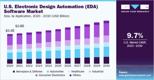
Electronic Design Automation Software Market Growth & Trends
The global electronic design automation software market size is anticipated to reach USD 22.21 billion by 2030, expanding at a CAGR of 9.1% from 2023 to 2030, according to a new study by Grand View Research Inc. The growing usage of advanced electronic components across different areas of healthcare, automotive, and consumer electronic sectors is driving Electronic Design Automation (EDA) software market growth. Apart from this, the proliferation of the Internet of Things (IoT) and connected devices further promotes EDA software market advancement.
Miniaturization of devices and chips is expected to create lucrative opportunities for EDA software. This software assists chipmakers in lowering the errors in Integrated Circuit (IC) and chips, thereby driving the electronic design automation software industry growth. The exponential growth of the integrated circuits market is driving the need for electronic design automation software. The software is increasingly being adopted for designing electronic systems such as printed circuit boards and integrated circuits, supporting the growth of the EDA market.
Furthermore, developments in technology, growing digitization, growth of the electronics manufacturing industry, and increasing adoption of advanced rendering & simulation tools by hardware designers are expected to positively influence the electronic design automation software industry growth over the forecast period. Furthermore, the increasing acceptance and awareness of smart fitness devices are factors enabling electronic design companies to invest in innovative design software tools for designing enhanced & compact products, thereby propelling the EDA software market growth over the forecast period.
Growing demand for EDA software is encouraging various market players to adopt various business strategies to achieve higher profitability in the market for electronic design automation software. Market players are unveiling new solutions by partnering with technology providers to improve their brand identity, propelling the EDA software market growth. For instance, in January 2022, Altium LLC announced a partnership with MacroFab, Inc., a U.S.-based cloud platform provider for electronic production, to launch “Altimade.” The new solution combines elastic manufacturing capabilities and real-time supply chain data, available on the Altium 365 electronic design platform. Altimade empowers customers to request instant quotes and place orders for manufacturing their PCB assembly without exiting the design environment.
Request a free sample copy or view report summary: https://www.grandviewresearch.com/industry-analysis/electronic-design-automation-eda-software-market
Electronic Design Automation Software Market Report Highlights
The services segment is expected to register a CAGR of 10.6% from 2023 to 2030. The segment growth can be attributed to the increasing proclivity of OEMs to outsource their design needs. Furthermore, electronic circuit boards are in high demand in the industry due to their increasing importance in a variety of vital electronic products such as mobile phones and tablets
The cloud segment is expected to register a CAGR of 10.8% from 2023 to 2030. Cloud-based deployment allows for faster distribution, less maintenance, lower costs, and more scalability
The healthcare segment is expected to register a CAGR of 11.5% from 2023 to 2030. The segment growth can be attributed to the benefits of EDA software in healthcare, such as lower costs, improved patient outcomes, faster design & development, enabled regulatory compliance of medical devices, and simulation and testing of medical equipment
The microprocessors & controllers segment is expected to register a CAGR of 9.5% from 2023 to 2030. The increased use of microprocessors in consumer devices such as smartphones, personal computers (PCs), and laptops is expected to drive global demand for the segment
Asia Pacific is anticipated to emerge as the fastest-growing region over the forecast period at a CAGR of 9.6%. A surge in demand for electronic devices together with the prevalence of key electronic component manufacturers in Greater China is expected to drive regional growth
Electronic Design Automation Software Market Segmentation
Grand View Research has segmented the global electronic design automation software market based on product, deployment, application, end-use, and region:
Electronic Design Automation (EDA) Software Product Outlook (Revenue, USD Billion, 2018 - 2030)
Computer-aided Engineering (CAE)
IC Physical Design and Verification
Printed Circuit Board and Multi-chip Module (PCB and MCM)
Semiconductor Intellectual Property (SIP)
Services
Electronic Design Automation (EDA) Software Deployment Outlook (Revenue, USD Billion, 2018 - 2030)
Cloud
On-premise
Electronic Design Automation (EDA) Software Application Outlook (Revenue, USD Billion, 2018 - 2030)
Aerospace and Defense
Automotive
Healthcare
Industrial
Consumer Electronics
Others
Electronic Design Automation (EDA) Software End-use Outlook (Revenue, USD Billion, 2018 - 2030)
Microprocessors & Controllers
Memory Management Unit (MMU)
Others
Electronic Design Automation (EDA) Software Regional Outlook (Revenue, USD Billion, 2018 - 2030)
North America
Europe
Asia Pacific
Latin America
Middle East & Africa
List of Key Players in the Electronic Design Automation Software Market
Advanced Micro Devices, Inc.
Aldec, Inc.
Altair Engineering Inc.
Altium LLC
Autodesk, Inc.
ANSYS, Inc.
Cadence Design Systems, Inc.
eInfochips
EMA Design Automation, Inc.
Keysight Technologies
Microsemi
Synopsys, Inc.
Silvaco, Inc.
The MathWorks, Inc.
Vennsa Technologies
Zuken
Browse Full Report: https://www.grandviewresearch.com/industry-analysis/electronic-design-automation-eda-software-market
#Electronic Design Automation Software Market#Electronic Design Automation Software Market Size#Electronic Design Automation Software Market Share
0 notes
Text
Rise of ASICs and GPUs: Driving the AI Chipset Revolution

The global Artificial Intelligence (AI) Chipset Market is undergoing remarkable growth, driven by rapid technological advancements, increasing adoption of AI-powered devices, and innovations in semiconductor design. This article delves into the key trends, market dynamics, and opportunities shaping the industry.
Market Overview
The AI Chipset Market was valued at US$ 45.5 billion in 2021 and is projected to expand at an impressive CAGR of 31.8% from 2022 to 2031, reaching a market value of US$ 717.4 billion by the end of 2031. This growth is fueled by the increasing demand for AI-enabled consumer electronics, advancements in edge and cloud computing, and ongoing investments in semiconductor R&D.
Key Drivers of Market Growth
1. Rise in AI Applications
AI chipsets play a crucial role in enhancing the performance of AI-powered devices such as smartphones, tablets, wearables, and smart home systems. The proliferation of smart devices has created a demand for chips capable of handling complex computations efficiently while consuming minimal power.
Leading smartphone manufacturers are now designing AI-based chips capable of executing trillions of operations per second. These chips enable advanced features such as AI image recognition, voice processing, and real-time data analytics.
2. Advances in Semiconductor Technology
Recent innovations in semiconductor design and manufacturing are transforming the AI hardware landscape. Companies are leveraging nodes below 28nm and adopting advanced packaging technologies to enhance speed, reduce latency, and optimize performance.
AI chipsets now require new materials, architectures, and manufacturing processes to meet the growing computational demands. The development of 3D chip configurations and integration of neural networks into hardware have further accelerated market growth.
3. Increasing Demand for Edge AI Chips
Edge-based AI chips are gaining traction due to their ability to process data locally, reducing the need for cloud connectivity. These chips are being integrated into a wide range of devices, from smartphones and wearables to robots and industrial machinery.
Edge AI chips offer significant benefits such as improved data security, reduced latency, and lower power consumption. While these chips are ideal for real-time processing, cloud-based AI chipsets remain essential for handling large-scale data operations.
Market Opportunities
1. Growth in Consumer Electronics
The consumer electronics industry is a major driver of AI chipset demand. From smart speakers and home appliances to autonomous vehicles, AI-powered devices are reshaping customer experiences. Companies are also developing general-purpose AI chips for diverse applications, including robotics and industrial automation.
2. Regional Market Trends
North America: The region is expected to dominate the global AI chipset market, driven by advancements in electronic design automation (EDA) tools and significant investments in AI research. The U.S. Chips Act of 2022 has further bolstered funding for AI and semiconductor projects.
Asia Pacific: As the largest market for consumer electronics and automotive, Asia Pacific is poised to grow at the highest CAGR during the forecast period. China, in particular, is emerging as a key player in AI hardware production, leveraging advanced manufacturing capabilities.
Competitive Landscape
The AI chipset market is characterized by intense competition among both established players and startups. Major companies, including NVIDIA, Intel, Alphabet (Google), IBM, Apple, Huawei, MediaTek, Baidu, and Graphcore, are investing heavily in R&D to develop cutting-edge solutions.
Notable Developments
Baidu launched its second-generation AI chip, Kunlun 2, designed for data-intensive applications such as autonomous driving.
Home appliance manufacturers like Midea Group are venturing into AI chip development to enhance supply chain stability and improve product performance.
Future Outlook
The Artificial Intelligence Chipset Market is set to revolutionize industries by enabling smarter, faster, and more efficient devices. From cloud computing and edge AI to advancements in semiconductor technology, the market holds immense potential for growth.
As businesses continue to adopt AI-powered solutions, the demand for specialized chipsets will only accelerate, driving innovation and creating new opportunities for market players.
Contact Us: Transparency Market Research Inc. CORPORATE HEADQUARTER DOWNTOWN, 1000 N. West Street, Suite 1200, Wilmington, Delaware 19801 USA Tel: +1-518-618-1030 USA - Canada Toll Free: 866-552-3453 Website: https://www.transparencymarketresearch.com Email: [email protected]
0 notes
Text
A blending of Artificial Intelligence (AI) with Semiconductors

Dr. Ipseeta Nanda
Professor, IILM University, Greater Noida
UP, India The integration of Artificial Intelligence (AI) with the semiconductor industry represents a transformative convergence that is reshaping the technological landscape by advancing chip design, optimizing manufacturing, and enabling AI-powered applications. Semiconductors are the foundational building blocks of modern computing devices, and their role in supporting AI has become increasingly critical as AI applications demand unprecedented computational power, efficiency, and scalability. At the design stage, AI technologies, such as machine learning algorithms, are being employed to enhance Electronic Design Automation (EDA) tools.
These AI-powered tools enable engineers to accelerate chip design processes by optimizing key parameters like performance, power efficiency, and area (PPA). AI algorithms are also capable of predicting potential design flaws early in the development cycle, significantly reducing the costly iterations traditionally associated with chip manufacturing. Moreover, generative AI is being explored to automate the creation of chip layouts, offering innovative design solutions that may not be immediately intuitive to human designers.
This not only shortens the time-to-market for advanced chips but also fosters creativity in architecture exploration. On the manufacturing side, AI-driven solutions are proving instrumental in optimizing semiconductor fabrication processes. Fabrication involves numerous intricate steps, from deposition and etching to lithography and packaging, each requiring precise control to ensure high yield and minimal defects. AI systems monitor these processes in real time, analyzing vast streams of data to identify inefficiencies or abnormalities that human operators might overlook. For example, predictive maintenance powered by machine learning can analyze sensor data from fabrication equipment to foresee potential malfunctions, allowing proactive measures to prevent costly downtime.
Similarly, advanced AI models are used in defect detection systems to analyze optical inspection data, classifying defects with a level of speed and accuracy that surpasses traditional rule-based systems. These advancements translate into higher manufacturing efficiency, reduced waste, and improved product quality, which are critical in a highly competitive industry.
Another important aspect of this integration is the development of AI-specific semiconductor architectures that enhance the performance of AI workloads. Traditional general-purpose CPUs are no longer sufficient to meet the demands of modern AI algorithms, which require massive parallel processing and high memory bandwidth. This has led to the emergence of specialized hardware such as Graphics Processing Units (GPUs), Tensor Processing Units (TPUs), and custom-designed Application-Specific Integrated Circuits (ASICs).
These chips are optimized to handle the intensive computations required for training deep neural networks and performing real-time inference. Beyond this, innovations in neuromorphic computing are paving the way for chips that mimic the structure and function of the human brain. Such architectures are especially promising for edge AI applications, where low latency and energy efficiency are paramount. Edge devices, including smartphones, smart sensors, and autonomous vehicles, are increasingly equipped with AI-optimized semiconductors that allow complex models to run locally without relying on cloud-based resources.
This not only reduces the time required for decision-making but also addresses privacy concerns by keeping data processing on-device. Furthermore, the symbiotic relationship between AI and semiconductors is enabling advancements in sectors like healthcare, automation, and telecommunications. In healthcare, for instance, AI-powered chips are revolutionizing medical imaging by enhancing the resolution and speed of imaging devices, leading to faster and more accurate diagnoses. Robotic surgery systems also benefit from AI-enabled chips that provide the computational power needed for precise, real-time control.
Similarly, in industrial automation, semiconductors designed for AI applications drive the intelligence behind smart factories, enabling predictive maintenance, quality control, and supply chain optimization. Telecommunications is another area where this blending is having a profound impact. AI algorithms, running on advanced semiconductors, are being used to optimize network performance in 5G systems, reducing latency and improving data throughput.
Figure: Enabling AI-Powered Solutions with Semiconductors
These innovations set the stage for the next generation of connectivity technologies, paving the way for even more complex and immersive AI applications. The co-design of hardware and software is another critical element in the successful blending of AI with semiconductors. Traditionally, hardware was developed independently of software, but the increasing complexity of AI workloads has necessitated a more integrated approach. AI models and semiconductor hardware are now being co-optimized to achieve the best possible performance. This involves tailoring chip architectures to specific machine learning tasks while simultaneously adapting AI algorithms to leverage hardware capabilities fully. This synergy not only boosts computational efficiency but also addresses one of the most pressing challenges in AI today: energy consumption.
Training and deploying AI models, particularly large-scale ones, require immense amounts of energy, and semiconductors designed with energy efficiency in mind are key to making AI more sustainable. Low-power designs, combined with innovations in cooling and power management, are helping to reduce the environmental impact of AI applications. Lastly, the feedback loop between AI and semiconductor development is creating a virtuous cycle of innovation.
AI algorithms are not only used to improve semiconductor design and manufacturing but also rely on advancements in semiconductor technology to evolve further. For example, as semiconductor manufacturing enables smaller and more efficient transistors, AI models can become more complex and capable, leading to breakthroughs in fields like natural language processing, computer vision, and autonomous systems. In turn, these advancements spur demand for even more sophisticated semiconductors, driving further innovation in the industry.
This dynamic interplay is accelerating the pace of technological progress, making AI and semiconductors mutually reinforcing pillars of the modern digital era. As AI continues to evolve, the semiconductor industry is poised to play an even more pivotal role in enabling its adoption across a broad spectrum of applications, from consumer electronics to critical infrastructure. The blending of AI with semiconductors, therefore, is not just a technological trend but a foundational shift that is shaping the future of innovation across multiple domains.
0 notes
Text
Global Cloud Electronic Design Automation Market Analysis 2024: Size Forecast and Growth Prospects
The cloud electronic design automation global market report 2024 from The Business Research Company provides comprehensive market statistics, including global market size, regional shares, competitor market share, detailed segments, trends, and opportunities. This report offers an in-depth analysis of current and future industry scenarios, delivering a complete perspective for thriving in the industrial automation software market.
Cloud Electronic Design Automation Market, 2024 report by The Business Research Company offers comprehensive insights into the current state of the market and highlights future growth opportunities.
Market Size - The cloud electronic design automation market size has grown strongly in recent years. It will grow from $7.37 billion in 2023 to $7.96 billion in 2024 at a compound annual growth rate (CAGR) of 7.9%. The growth in the historic period can be attributed to advanced simulation capabilities, integration with other cloud services, accessibility, enhanced security.
The cloud electronic design automation market size is expected to see strong growth in the next few years. It will grow to $10.7 billion in 2028 at a compound annual growth rate (CAGR) of 7.7%. The growth in the forecast period can be attributed to AI and machine learning integration, 5G and IoT growth, customization and personalization, cybersecurity enhancements, quantum computing integration. Major trends in the forecast period include AI-driven design automation, technological advancements, containerization and orchestration, multi-cloud and hybrid cloud architectures, predictive analytics and simulation.
Order your report now for swift delivery @ https://www.thebusinessresearchcompany.com/report/cloud-electronic-design-automation-global-market-report
Scope Of Cloud Electronic Design Automation Market The Business Research Company's reports encompass a wide range of information, including:
1. Market Size (Historic and Forecast): Analysis of the market's historical performance and projections for future growth.
2. Drivers: Examination of the key factors propelling market growth.
3. Trends: Identification of emerging trends and patterns shaping the market landscape.
4. Key Segments: Breakdown of the market into its primary segments and their respective performance.
5. Focus Regions and Geographies: Insight into the most critical regions and geographical areas influencing the market.
6. Macro Economic Factors: Assessment of broader economic elements impacting the market.
Cloud Electronic Design Automation Market Overview
Market Drivers - The increasing demand for automation is expected to propel the growth of the cloud electronic design automation (EDA) market going forward. Automation refers to the technique of making an apparatus, a process, or a system operate automatically, utilizing machines and computers that can operate without needing human control. Automation is experiencing a surge in adoption driven by its potential to revolutionize productivity, streamline processes, and reduce costs across industries. Automation is helpful in cloud electronic design automation (EDA) by enabling the creation of cloud-native EDA tools and pre-optimized hardware platforms that can operate without needing human control. For instance, in June 2022, according to Salesforce, a US-based cloud-based software company, in partnership with Vanson Bourne, demand for automation has surged in over 90% of companies. The survey included 600 CIOs and IT decision-makers from global enterprises, and the highest demand for automation came from departments such as research and development, administrative/operations, customer service, and marketing. Therefore, the increasing demand for automation is driving the growth of the cloud electronic design automation (EDA) market.
Market Trends - Major companies operating in the cloud electronic design automation market are developing advanced technologies, such as disruptive cloud-based SaaS solution to drive their revenues in the market. A disruptive cloud-based SaaS solution is a software-as-a-service (SaaS) solution that leverages cloud computing to transform an industry or market by providing easy access to powerful tools. For instance, in April 2022, Synopsys Inc, a US-based electronic design automation company, launched disruptive cloud-based Software-as-a-Service (SaaS) solution called synopsys cloud 4.0, aimed at transforming the chip development. This cloud-based SaaS solution aims to accelerate and democratize chip design by providing easy access to powerful tools and resources, thereby helping semiconductor companies to innovate faster, leaner, and more efficiently.
The cloud electronic design automation market covered in this report is segmented –
1) By Type: Computer Aided Engineering, Semiconductor Intellectual Property, IC Physical Design And Verification, Printed Circuit Board and Multi-Chip Module 2) By Deployment Model: Public Cloud, Private Cloud, Hybrid Cloud 3) By Vertical: Automotive, Consumer Electronics, Aerospace And Defense, Industrial, Healthcare, Telecommunication
Get an inside scoop of the cloud electronic design automation market, Request now for Sample Report @ https://www.thebusinessresearchcompany.com/sample.aspx?id=14068&type=smp
Regional Insights - North America was the largest region in the cloud electronic design automation market in 2023. Asia-Pacific is expected to be the fastest-growing region in the forecast period. The regions covered in the cloud electronic design automation market report are Asia-Pacific, Western Europe, Eastern Europe, North America, South America, Middle East, Africa.
Key Companies - Major companies operating in the cloud electronic design automation market are Siemens AG, Sonnet Software Inc., Dolphin Design, OneSpin Solutions GmbH, Real Intent Inc., Concept Engineering GmbH, Blue Pearl Software Inc., Agnisys Inc, Agilent technologies , Dassault Systèmes, Tektronix, Inc., Keysight Technologies, Synopsys Inc., Autodesk Inc, Cadenece Design System, Forte Design Systems, Xilinx Inc., ANSYS Inc., Frontline PCB Solutions, CircuitSutra Technologies Pvt. Ltd., JEDA Technologies, Mentor Graphics Corporation, Nimbic Inc., Lattice Semiconductor Corporation, AWR Corporation, Zuken Inc., Tanner EDA, Empyrean Software
Table of Contents 1. Executive Summary 2. Cloud Electronic Design Automation Market Report Structure 3. Cloud Electronic Design Automation Market Trends And Strategies 4. Cloud Electronic Design Automation Market ��� Macro Economic Scenario 5. Cloud Electronic Design Automation Market Size And Growth ….. 27. Cloud Electronic Design Automation Market Competitor Landscape And Company Profiles 28. Key Mergers And Acquisitions 29. Future Outlook and Potential Analysis 30. Appendix
Contact Us: The Business Research Company Europe: +44 207 1930 708 Asia: +91 88972 63534 Americas: +1 315 623 0293 Email: [email protected]
Follow Us On: LinkedIn: https://in.linkedin.com/company/the-business-research-company Twitter: https://twitter.com/tbrc_info Facebook: https://www.facebook.com/TheBusinessResearchCompany YouTube: https://www.youtube.com/channel/UC24_fI0rV8cR5DxlCpgmyFQ Blog: https://blog.tbrc.info/ Healthcare Blog: https://healthcareresearchreports.com/ Global Market Model: https://www.thebusinessresearchcompany.com/global-market-model
0 notes
Text
Agnisys at DVCon India 2024: Empowering Innovation in Design and Verification

The Design and Verification Conference DVCon India 2024 promises to be a pivotal event in the electronic design automation (EDA) industry. Known for bringing together innovators, engineers, and thought leaders, DVCon India is a key platform for discussing emerging trends, technologies, and methodologies in the design and verification space. This year, one of the standout participants is Agnisys, a company renowned for its groundbreaking solutions in IP development, design, and verification automation.
Who is Agnisys?
Agnisys, Inc. has earned a stellar reputation for its cutting-edge tools designed to automate the design, verification, and implementation of intellectual property (IP), registers, and system-on-chip (SoC) architectures. As industries increasingly demand higher levels of innovation and performance, Agnisys has consistently been at the forefront of providing robust automation solutions to help semiconductor companies streamline their development processes.
The company's tool suite, which includes IDesignSpec and other automation products, has gained traction globally by enhancing the productivity of design and verification engineers. With a strong focus on user-friendly tools, Agnisys aims to reduce the manual effort and errors in designing complex systems, ultimately shortening time-to-market.
The Theme of Agnisys at DVCon India 2024
At DVCon India 2024, Agnisys will focus on the theme of "Empowering Innovation in Design and Verification Automation." Agnisys will showcase how its comprehensive solutions can help teams achieve higher efficiency and accuracy in their design and verification processes. The company’s tools are designed to automate critical tasks, making it easier for engineers to handle the increasing complexity of SoC development and register management.
Highlights of Agnisys' Participation
1. Technical Sessions
Agnisys will host several technical sessions during DVCon India 2024, aimed at educating attendees about the latest advancements in automation for design and verification. These sessions will cover topics such as:
Automating Register and IP Design: A demonstration of how IDesignSpec™ enables the automated generation of register files and verification environments, ensuring consistency between design and documentation.
Enhancing UVM Verification: Agnisys will present how their tools integrate with Universal Verification Methodology (UVM) environments to automate the generation of testbenches and improve coverage.
AI and Machine Learning in EDA: Agnisys will explore how artificial intelligence (AI) and machine learning (ML) can be leveraged to enhance verification processes, optimize design flows, and predict verification coverage gaps.
2. Live Demonstrations
In addition to the technical sessions, Agnisys will offer live demonstrations of its tools at their booth. Attendees can get a firsthand look at how these tools can be used to streamline design and verification tasks.
IDesignSpec™: The flagship tool that enables specification-driven design and verification of registers and IP blocks.
DVinsight: A tool focused on improving functional coverage and verification through automated insights.
These demonstrations will provide an interactive platform for engineers and decision-makers to see how Agnisys' solutions can be customized to fit their unique needs.
3. Panel Discussions
Agnisys experts will participate in panel discussions alongside other leaders in the EDA space. These panels will explore current industry challenges such as managing verification complexity in modern SoCs and how automation can help address these issues. Agnisys will offer its perspective on how its tools are helping to shape the future of design and verification.
4. Networking Opportunities
DVCon India 2024 will also provide numerous networking opportunities for attendees to engage with Agnisys’ experts. Whether it’s through Q&A sessions following the technical presentations or more informal discussions at the booth, engineers will have ample opportunity to exchange ideas with the Agnisys team and gain insights on how to improve their design and verification processes.
Why Agnisys Matters to the Industry
The semiconductor industry is experiencing rapid growth, with an increasing demand for more powerful and efficient chips. This has led to an increase in the complexity of SoC architectures, placing enormous pressure on design and verification teams to meet time-to-market deadlines. Agnisys addresses these challenges head-on by automating repetitive tasks, reducing human errors, and ensuring consistency across the design flow.
Moreover, Agnisys’ solutions are designed to integrate seamlessly into existing workflows, making it easier for teams to adopt their tools without a significant learning curve. Their tools provide a significant boost in productivity, making it possible to manage larger, more complex designs within shorter timeframes.
The Future with Agnisys
As the demands on chip design and verification teams continue to grow, the need for robust automation tools will become even more critical. Agnisys is committed to pushing the boundaries of innovation in this space, and its participation in DVCon India 2024 is a testament to its leadership in the field.
With the ability to automate essential aspects of SoC design, verification, and IP management, Agnisys is well-positioned to remain a key player in the industry. Their tools not only improve efficiency but also empower engineers to focus on the more creative aspects of their work, leading to faster, more reliable innovations.
In conclusion, Agnisys' presence at DVCon India 2024 will showcase its continued commitment to transforming the design and verification landscape. By attending the event, engineers, managers, and decision-makers can learn how Agnisys' automation solutions are driving the future of the semiconductor industry.
0 notes
Text
Electronic Design Automation Market Will Reach USD 31,121.1 Million by 2030
The total value of theglobal electronic design automation market was USD 14,109.5 million in 2022, and it will rise at a growth rate of above 10.4% over this decade, reaching USD 31,121.1 million by 2030. This is mainly because of the growing difficulty of electronic systems and the requirement for effective design tools.

Moreover, a count of industries has contributed to the industry growth by creating unique design specifications, like healthcare, telecommunications, consumer electronics, and automotive. This generates the requirement for modified design solutions.
The semiconductor sector has gained traction headway in contracting procedure nodes, therefore fortifying the growth of more modest and power-capable ICs. The requirement to decrease power usage and heat dissipation and, yet, uphold signal integrity makes design problems, as a result of this reduction. Electronic design automation apparatus offers the vital capacities to confront such issues and advance the IC design for compact interaction nodes.
The growing difficulty of electronic design automation requires dedicated knowledge to make and improve such systems. Designers and engineers with the expertise and capability to manage complex designs are in high demand among the industries in the industry. As a result, there is a requirement for skilled specialists, which can surge the competition for talent.
In 2022, on the basis of application, the consumer electronics category had the largest share, of around 30%, in the electronic design automation industry, and the category is projected to dominate in the future as well. This is mainly due to the advent of more-urbane electronics, because of the increasing demand for pioneering smartphones, smartwatches, and smart TVs, Therefore, the growing per-capita income across the globe is estimated to boost the category’s growth at a robust rate over the projection period.
On the basis of region, the APAC region is dominating with a 40% market share, and the region is projected to remain dominant in the future as well. This is mainly because of the increasing requirement for electronic devices, growing acceptance of developing technologies, like AI, IoT, and 5G; and the robust attention being paid to invention and R&D. The APAC region is a major user of EDA solutions as multifaceted semiconductor chips need sophisticated EDA tools for design and expansion.
APAC, specifically Japan, China, South Korea, and Taiwan, has long catered as substantial centers for the manufacturing of electronics. Semiconductor foundries, Consumer electronics industries, and creators of electronic components for other bigger systems are all well-represented in the region. The requirement for EDA solutions to allow the design and making of electronic systems is propelled by this manufacturing strength.
Hence, the growing difficulty of electronic systems and the requirement for effective design tools, are the major factors propelling the electronic design automation market.
Source: P&S Intelligence
1 note
·
View note
Text

Electronic Design Automation (EDA) Tools Market size at USD 11.62 billion in 2023. During the forecast period between 2024 and 2030, BlueWeave expects the Global Electronic Design Automation (EDA) Tools Market size to grow at a CAGR of 6.96% reaching a value of USD 17.4 billion by 2030. Global Electronic Design Automation (EDA) Tools Market is driven by increasing semiconductor complexity, demand for high-performance electronic devices, and the rise of IoT and AI applications. A growing emphasis on reducing time-to-market and production costs, coupled with advancements in semiconductor manufacturing processes, fuels the adoption of EDA tools. Additionally, the push for 5G technology, automotive electronics, and smart devices contributes to market growth. The expansion of the global electronics industry and the need for efficient design solutions to address intricate circuit designs and power consumption challenges further propel the EDA tools market, ensuring ongoing innovations and competitiveness in the semiconductor industry.
Opportunity – Increasing adoption of AI and ML in EDA tools
Global Electronic Design Automation (EDA) Tools Market is experiencing robust growth driven by the increasing adoption of Artificial Intelligence (AI) and Machine Learning (ML) within EDA tools. The integration enhances design efficiency, accelerates product development cycles, and optimizes performance, thereby attracting widespread interest from industries. The synergy of AI and EDA tools is revolutionizing electronic design processes, fostering innovations, and contributing significantly to the market expansion.
Impact of Escalating Geopolitical Tensions on Global Electronic Design Automation (EDA) Tools Market
Escalating geopolitical tensions, notably the Russia-Ukraine war, have significantly impacted the Global Electronic Design Automation (EDA) Tools Market. Supply chain disruptions heightened trade uncertainties, and increased production costs have impeded the seamless flow of EDA tools. The conflict has intensified concerns about resource availability, with key components being sourced from affected regions. Additionally, economic sanctions and geopolitical instability have led to decreased investor confidence, hindering market growth. The EDA market faces challenges in maintaining operational continuity, and strategic planning is crucial to navigating the turbulent geopolitical landscape, ensuring resilience and adaptability in the face of ongoing global uncertainties.
Sample Request @ https://www.blueweaveconsulting.com/report/electronic-design-automation-tools-market/report-sample
0 notes
Text
Advance Your Semiconductor Career Comprehensive VLSI Physical Design Courses
For engineers and students aiming to specialize in one of the most critical and in-demand fields of semiconductor engineering, Takshila Institute of VLSI Technologies in India offers a robust selection of expertly crafted VLSI physical design courses and flexible physical design course online programs. With the semiconductor industry rapidly advancing, professionals skilled in physical design are crucial in transforming logical circuit designs into manufacturable layouts on silicon.
Recognizing this demand, Takshila Institute delivers a deep and practical curriculum that empowers learners to master every stage of the physical design flow—from floorplanning and placement to clock tree synthesis, routing, and signoff processes. The institute’s VLSI physical design courses are meticulously designed to equip participants with hands-on expertise using industry-standard Electronic Design Automation (EDA) tools, enabling them to work confidently on real-world design projects.
These courses cover essential topics such as static timing analysis, design rule checks, layout versus schematic checks, and low power design techniques, ensuring that students acquire both the theoretical foundation and practical skills needed to excel in semiconductor companies. For learners who require flexibility due to work commitments or geographical constraints, Takshila Institute’s physical design course online offers a comprehensive and interactive learning experience.
Delivered through live virtual classes, recorded sessions, practical labs, and project work, the online program ensures that students receive the same rigorous training as in-person classes. The online format is designed to cater to working professionals, fresh graduates, and engineering students who want to upgrade their skills without compromising their current responsibilities. With mentorship from highly experienced faculty members, participants in the online course receive personalized guidance, technical doubt-clearing sessions, and project feedback to ensure deep understanding and skill mastery.
In addition to technical training, Takshila Institute emphasizes career readiness by offering placement assistance, resume building workshops, and mock interviews, giving students a competitive edge in the job market. The institute’s strong industry connections and focus on real-time project exposure make it a preferred choice for those seeking to specialize in VLSI physical design courses.
By enrolling with Takshila Institute of VLSI Technologies, students embark on a learning journey that not only deepens their technical capabilities but also prepares them to meet the challenges of modern semiconductor design. Whether through classroom learning or the convenient physical design course online, Takshila Institute stands as a trusted partner in building a successful career in VLSI physical design.
0 notes
Text
Electronic design automation (EDA) workloads: using IBM Cloud

A market sector known as Electronic design automation(EDA) is made up of hardware, software, and services that are used to help define, plan, design, implement, verify, and then manufacture semiconductor devices (or chips). Foundries or fabs that produce semiconductors are the main suppliers of this service.
EDA solutions are essential in three aspects even if they are not directly engaged in the production of chips:
To make sure the semiconductor manufacturing process produces the necessary performance and density, EDA tools are employed in its design and validation.
EDA tools are used to confirm that a design satisfies every criterion related to the manufacturing process. We call this area of study “design for manufacturability” (DFM).
The need to track the chip’s performance from the point of manufacture to field deployment is becoming more and more pressing. The term “silicon lifecycle management” (SLM) describes this third use.
EDA HPC environments are constantly expanding in size because to increased competition, the need to get products to market more quickly, and the growing demands for computers to handle the more fidelity simulations and modeling workloads. Businesses are trying to figure out how to effectively leverage technologies like hybrid cloud, accelerators, and containerization to obtain a competitive computing advantage.
The integrated circuit design and Electronic design automation software
In order to shape and validate state-of-the-art semiconductor chips, optimize their manufacturing processes, and guarantee that improvements in performance and density are reliably and consistently realized, Electronic design automation (EDA) software is essential.
For startups and small enterprises looking to enter this industry, the costs of purchasing and maintaining the computer environments, tools, and IT know-how required to use Electronic design automation tools pose a substantial obstacle. In addition, these expenses continue to be a major worry for well-established companies that use EDA designs. A key component of success is meeting deadlines, and chip designers and manufacturers are under tremendous pressure to introduce new chip generations with improved density, dependability, and efficiency.
Read more on Govindhtech.com
0 notes
Text
How to Apply Machine Learning and Artificial Intelligence in VLSI Design and Verification?
The world of VLSI design and verification is evolving rapidly, driven by technological advancements that demand more efficient and reliable solutions. Machine Learning (ML) and Artificial Intelligence (AI) have emerged as powerful tools in this field, promising to revolutionize the way we approach VLSI design and verification. In this blog, we will explore the application of ML and AI in VLSI, highlighting their methods, potential, and future trends.
Introduction
VLSI design and verification entail creating complex integrated circuits and ensuring their functionality. ML and AI are becoming indispensable in these processes, offering innovative solutions to longstanding challenges.
Machine Learning and Artificial Intelligence Methods for VLSI Design
Layout Optimization:
ML and AI can optimize the layout of VLSI circuits by considering various design parameters. They can achieve a higher level of performance, power efficiency, and manufacturability.
EDA Tool Enhancement:
Electronic Design Automation (EDA) tools are essential in VLSI design. ML and AI can enhance these tools by improving algorithms for place-and-route, timing analysis, and even suggesting design rule checks.
Predictive Analytics:
AI can predict potential design flaws, reducing the likelihood of errors and costly redesigns. It can analyze historical data to anticipate issues in the early stages of design.
Automatic Floorplanning:
Floorplanning is a crucial step in VLSI design. AI algorithms can automate floorplanning by optimizing the placement of functional blocks to achieve better performance and power efficiency.
Machine Learning and Artificial Intelligence Methods for VLSI Verification
Automated Testbench Generation:
Creating a testbench for VLSI verification is a time-consuming task. ML and AI can automate the testbench generation process, increasing the efficiency of verification.
Anomaly Detection:
ML algorithms can identify anomalies in simulation results, helping to pinpoint design flaws or unexpected behavior. This is particularly useful for uncovering hard-to-detect bugs.
Coverage Analysis:
AI techniques can analyze coverage data to ensure comprehensive testing. They can identify untested scenarios and guide verification engineers in creating more robust testbenches.
Formal Verification:
Formal verification is a mathematically rigorous method for proving correctness. ML and AI can enhance formal methods by making them more scalable and efficient.
Future Trends and Opportunities of Machine Learning and Artificial Intelligence in VLSI Design and Verification
Customized Design:
AI can lead to highly customized designs optimized for specific applications. This opens opportunities in domains like IoT, automotive, and healthcare where specialized chips are in demand.
Real-time Verification:
ML can enable real-time verification during the design process. Engineers can receive immediate feedback on potential issues, reducing design iterations.
Reduced Time to Market:
With ML and AI accelerating design and verification processes, the time to market for VLSI products can be significantly reduced, giving companies a competitive edge.
Design Space Exploration:
AI can explore a broader design space, uncovering innovative solutions that might not be evident to human designers.
Safety and Security:
ML and AI can enhance VLSI security by identifying vulnerabilities and potential attacks, crucial in our interconnected world.
Conclusion
The integration of Machine Learning and Artificial Intelligence in VLSI design and verification is a promising development. These technologies hold the potential to optimize designs, accelerate the verification process, and enable the creation of highly specialized and efficient circuits. The future of VLSI design and verification is closely intertwined with the continued advancements in ML and AI.
If you are curious to know more about VLSI and wish to start a career in the VLSI industry then check out the Job-oriented VLSI courses from Maven Silicon VLSI training institute.
0 notes
Text
Global Electronic Design Automation Tools (EDA) Market (2021 to 2027) – Industry Trends, Share, Size, COVID-19 Impact, Growth, Opportunity and Forecasts
The global electronic design automation tools market is anticipated to grow at 9.48% CAGR during 2021-2027 owing to the rising demand for complex integrated circuits (ICs), technologically developed consumer electronics, increasing precision of semiconductor devices, rising adoption of FinFET architecture to design modern processors, increasing penetration of IoT, AI, and VR, and increased adoption of connected devices will fuel the growth in the region. The expansion of cloud computing platforms and the rising complexity of SoC designs will spur the growth of the EDA software market. The EDS tools are helping chip manufacturing companies to design and manufacture complex chips at less cost in a short span of time. Nevertheless, the industry verticals are rapidly using IC design and verification tools to perform the placement and routing of circuits automatically on an IC or ASIC, thereby boosting the market of the electronic design automation (EDA) tools.
The COVID-19 outbreak has had an adverse impact on the electronic design automation (EDA) tools market which has resulted in decreasing subscription of electronic design automation. However, the demand is anticipated to rise owing to the rising production volume of semiconductor chips.
Request to get a free sample copy at https://www.vynzresearch.com/ict-media/electronic-design-automation-eda-tools-market/request-sample
Based on product type, the global EDA tools market is divided into printed circuit board (PCB) and multi-chip module (MCM), computer-aided engineering (CAE), semiconductor intellectual property (SIP), IC physical design & verification, and services. The IC physical design & verification segment is anticipated to have a high CAGR during 2021-2027 owing to the rising complexity of IC designs and mounting demand to provide high accuracy and precision in semiconductor devices. Thus IC design & verification will automatically perform the placement and routing of circuits on an IC or ASIC.
North America dominates the electronic design automation tools market owing to the adoption in various industries like consumer electronics, automotive, etc., and the increased advancement in the semiconductor industry and circuit manufacturing industry. Moreover, the presence of industry players like Ansys, Inc., Cadence Design Systems Inc., etc and continuous investment to upgrade the offerings and expansion will fuel the growth of Electronic Design Automation Tools in the region.
August 2021, Cadence Design Systems, Inc. and Tower Semiconductor have partnered to launch a silicon-verified SP4 TRFSOI switch reference design flow via the Virtuoso Design Platform and RF solutions The flow determines the advantages of having a unified design environment for chip and package co-design.
The key players in the electronic design automation (EDA) tools industry: Synopsys, Cadence Design Systems Inc., Mentor Graphics, Zuken, EEsoF.
Source: VynZ Research

#electronic design automation tools (eda) market#electronic design automation tools (eda) market size#electronic design automation tools (eda) market forecast#Electronic Design Automation Tools (EDA) Market Demand
0 notes
Text
Europe Cartridge Heating Coil Market Size Growth Set to Surge Significantly during 2022-2030
"https://tealfeed.com/sanitary-household-paper-market-pointing-capture-hwvvs https://tealfeed.com/elevator-door-2022-market-huge-growth-bqrbg https://tealfeed.com/allulose-cas-551-68-8-market-k8cdk https://tealfeed.com/in-memory-database-market-expected-boom-qs1wg https://tealfeed.com/video-streaming-market-size-scope-top-iicjp https://tealfeed.com/smart-container-market-size-outlook-2027-bvcn8 https://tealfeed.com/electronic-grade-polysilicon-market-2022-pointing-rm2fk https://tealfeed.com/methyl-bromoacetate-market-size-analysis-leading-mowox https://tealfeed.com/vegan-protein-bar-market-size-set-guos1 https://tealfeed.com/multifactor-authentication-mfa-market-size-growth-ahdpg https://tealfeed.com/inorganic-zinc-rich-primers-market-expecting-dijuf https://tealfeed.com/packaged-ready-made-salads-market-2022-pxtt0 https://tealfeed.com/modified-starch-market-report-covers-future-p4mr0 https://tealfeed.com/chromatic-harmonicas-market-growth-trends-size-bh1rp https://tealfeed.com/grass-fed-beef-market-challenges-opportunities-qg9uk https://tealfeed.com/rotary-hammer-drill-market-overview-demand-ema4f https://tealfeed.com/2022-open-source-performance-testing-market-adv7h https://tealfeed.com/mushrooms-truffles-market-outlook-post-covid-5koid https://tealfeed.com/agro-rural-tourism-market-huge-growth-ob8xe https://tealfeed.com/prometryn-cas-7287-19-6-market-esjpl https://tealfeed.com/colocation-market-2022-demand-future-scope-jrgts https://tealfeed.com/liquid-saturated-polyester-resin-market-2022-u56xz https://tealfeed.com/electronic-design-automation-eda-market-global-lhaaj https://tealfeed.com/normal-phase-columns-market-size-growth-7tbkd https://tealfeed.com/contact-center-transformation-market-2022-top-vsqzo https://tealfeed.com/health-products-industry-future-demand-market-ozyok https://tealfeed.com/pediatric-epilepsy-therapeutics-market-size-historical-wdpus https://tealfeed.com/garden-sheds-market-industry-analysis-segments-4yr8r https://tealfeed.com/blockchain-insurance-market-future-scope-demands-cmhph https://tealfeed.com/vulnerability-scanner-software-market-2022-analysis-adx2c https://tealfeed.com/isoxaflutole-cas-141112-29-0-market-mkwju https://tealfeed.com/hybrid-street-lighting-systems-market-witness-hgf6d https://tealfeed.com/pool-table-blanket-market-next-big-o7wim https://tealfeed.com/browser-game-market-2022-2027-thriving-cm2jf https://tealfeed.com/new-report-caulking-tools-market-2022-ofigt https://tealfeed.com/printing-software-market-current-business-trends-jljem https://tealfeed.com/indoor-skis-market-demand-future-scope-2392u https://tealfeed.com/pressure-relief-devices-hi-tech-device-emnzq https://tealfeed.com/nano-nickel-industry-future-demand-market-cykrs https://tealfeed.com/toggle-switches-market-2022-latest-sales-h7tsw https://tealfeed.com/electronics-manufacturing-services-ems-market-2022-lwvbc https://tealfeed.com/temozolomide-market-2022-top-key-players-ix0hg https://tealfeed.com/polyurethane-sealants-market-2022-omicron-covid19-xzhov https://tealfeed.com/dialysis-market-size-share-trend-complete-r8lvm https://tealfeed.com/emv-market-covid19-omicron-updated-expecting-jdjgl https://tealfeed.com/digital-english-language-learning-market-growth-uteen https://tealfeed.com/aloe-vera-extracts-market-witness-huge-ppl58 https://tealfeed.com/automotive-intake-manifold-market-pointing-capture-ymm1c https://tealfeed.com/maple-syrup-2022-market-huge-growth-q2t2t https://tealfeed.com/basketball-training-equipment-market-2022-challenges-p8pix https://tealfeed.com/low-voltage-switchgear-market-expected-boom-len7y https://tealfeed.com/arts-crafts-market-size-scope-top-1jip7 https://tealfeed.com/assessment-services-market-size-outlook-2027-hljug https://tealfeed.com/essential-oils-market-2022-pointing-capture-ritys https://tealfeed.com/metal-cladding-market-size-analysis-leading-psqtl
0 notes
Text
Global Electronic Design Automation Market Research, Size, Witness Stunning Growth By 2028 | The Insight Partners
The Electronic Design Automation Market accounted to US$10.31 Bn in 2018 and is expected to grow at a CAGR of 12.0% during the forecast period 2019 – 2027, to account to US$28.27 Bn by 2027.
The major reason for this is the huge electronics and semiconductor hub in China coupled with the large population density of the region. Also China accounts for the largest shipments for semiconductors across the world, the new market initiatives and strategic partnerships are expected to continue during the forecast period, contributing to high growth of electronic design automation market in the region
Rising complexities and cost challenges faced by the industries for implementation of expensive complex designs is key influencer driving the demand of advanced EDA (Electronic Design Automation) tools. The EDA software are specifically designed for electronic systems that includes printed circuit boards and integrated circuits. The tools offered by this software function collaboratively in a design flow, which is further used by the chip designers for designing an analysis of entire semiconductor chips. As the modern semiconductor chips comprises of myriad components and complex designs, the EDA tools have become an essential for the designers.
Get Sample PDF:
Europe is anticipated to witness the fastest growth rate over the forecast period. Europe being a technologically advanced region, bags immense investment opportunities. Further, the growth in innovation and research on electronic devices in Europe is projected to remarkably contribute towards the growth of EDA market during the forecast period. Further, robust automotive industry and ongoing technological developments is opportunistic for the market in the region.
The market in the recent years witnessed several partnerships amid end-user industries. The trail of partnerships in the EDA software market in past few years has therefore paved the growth opportunity for market. For instance in November 2018, Keysight Technologies, Inc. partnered with ON semiconductor for facilitating EDA services in order to empower its devices. Furthermore, in June 2018 Siemens had announced its partnership with Synopsys, Inc. on a wide range of electronic design automation (EDA) product interoperability projects for the benefit of their mutual customers. The collaboration spans a number of EDA domains from design to verification.
Buy Now: https://www.theinsightpartners.com/buy/TIPTE100001022/
Key findings of the study:
Asia-Pacific is anticipated to account the largest electronic design automation market share and would register a CAGR of 13.0%
Based on the type, SIP is projected to dominate the electronic design automation market
Consumer electronics led the electronic design automation market by application in 2018
The companies operating in the field of electronic design automation include Agnisys Inc., Aldec, Inc., Autodesk, Inc., Cadence Design Systems, Inc., Labcenter Electronics Ltd., Keysight Technologies, Mentor Graphics Corporation, Silvaco, Inc., Synopsys, Inc., and Zuken Inc. among others. Various other companies operating in the market and are coming up with new technologies and offerings which is helping the market for electronic design automation to expand over the years.
About Us:
The Insight Partners is a one stop industry research provider of actionable intelligence. We help our clients in getting solutions to their research requirements through our syndicated and consulting research services. We specialize in industries such as Semiconductor and Electronics, Aerospace and Defense, Automotive and Transportation, Biotechnology, Healthcare IT, Manufacturing and Construction, Medical Device, Technology, Media and Telecommunications, Chemicals and Materials.
Contact Us:
If you have any queries about this report or if you would like further information, please contact us:
Contact Person: Sameer Joshi
E-mail: [email protected]
Phone: +1-646-491-9876
0 notes
Text
Electronic Design Automation (EDA) Tools Market is Expected to Reach USD 19.1 Billion by the End of 2027
VynZ Research provides market overview of the current environment as well as the industry's future growth in the Electronic Design Automation (EDA) Tools market. It uses data from annual reports, product literature, industry developments, and other sources to conduct a quantitative market study. The future growth prospects of the industry are based on a rapid quantitative and qualitative assessment of data from various sources.
The Electronic Design Automation (EDA) Tools market is projected to reach USD 19.1 billion by 2027, witnessing a CAGR of 9.48 % during the forecast period 2021-2027.
To assist companies in developing their business plans, the research examines the major factors influencing the growth of the Electronic Design Automation (EDA) Tools market, also including Drivers, Constraints, Governmental Policies, Opportunities, Challenges, a Constructive Approach, and Market Economic Expansion Strategies.
Get a free sample copy of this market research @ https://www.vynzresearch.com/ict-media/electronic-design-automation-eda-tools-market/request-sample
The influence of recent market disruptions such as the Russia-Ukraine war and Covid-19 on the market will be examined in this research report.
Segments Defined:
The research report divides the market into segments based on geography, by Type, by Product Type and by Application During the forecast period of 2021 to 2027, each category gives data on production and consumption. Understanding the segments aids in determining the importance of various market growth variables.
Market segmentation:
Insight by Type
On the basis of type, the EDA tools market is bifurcated into on-premise solutions and cloud-based solutions. Between these two market segments, on-premise solutions are expected to grow faster during the forecast period. On-premises solutions are considered to be a flexible, safe, and reliable choice that can help business enterprises effectively manage funds, time, and resources into their core business strategies. The emerging cloud-based solutions will spur the demand for the EDA tools market. The increase in complexity of SoC designs emphasized the need to add new features and compute power to designs which can be done by cloud-based solutions as it offers scalability functionality.
Insight by Product Type
On the basis of product type the global EDA tools market is segmented into printed circuit board (PCB) and multi-chip module (MCM), computer-aided engineering (CAE), semiconductor intellectual property (SIP), IC physical design & verification, and services. Semiconductor intellectual property is expected to generate the highest revenue as it is considered a reusable functional unit that develops various building blocks in chip manufacturing through multi-vendor licensing. Furthermore, the extensive growth of the semiconductor IP segment is contributing to the growth of the global EDA tools market.
The integrated circuit (IC) physical design & verification segment is anticipated to exhibit a significant growth rate during the forecast period, owing to the increase in complexity of IC designs and surge in demand for great accuracy and precision of semiconductor devices. Additionally, end-users are increasingly adopting EDA IC design and verification tools to automate the design and routing of circuits in integrated circuits or application-specific integrated circuits (ASIC).
Insight by Application
The EDA tools market on the basis of application is categorized into consumer electronics, aerospace & defense, medical, industrial, automotive, telecommunications, and others. Among all these market segments, the telecommunications segment is expected to generate the highest revenue during the estimated period. EDA tools are being widely used by many companies in the industry to provide effective and efficient high-quality communication systems. In addition, it is observed that the rise in usage of mobile devices in emerging and advanced economies is promoting the use of EDA by various enterprises, thereby strengthening the growth of the global EDA tool market.
Region and Country Specific Defined:
Thorough research of certain regions and their related countries is conducted to guarantee that the comprehensive detailing of the Electronic Design Automation (EDA) Tools market's footprint and sales demographics are captured with accuracy, allowing users to make the most of this data.
Competitive Scenario:
In order to obtain essential and critical industry data, the records of major market participants are analyzed. It provides vital information and status on industry players, as well as serves a useful source of advice for businesses and organizations. Porter's Five Forces analysis, SWOT analysis, PEST analysis, competitor landscape, development trends, and strategy analysis, are all covered in depth in the "Electronic Design Automation (EDA) Tools market" research. Major breakthroughs, developments, mergers and acquisitions, and agreements with other important organizations have all been investigated.
Top players are:
EDA tools market include Synopsys, Cadence Design Systems inc., Mentor Graphics, Zuken, EEsoF.
FAQ
What are the trends and market dynamics along with market size and growth rate of the Electronic Design Automation (EDA) Tools market during the forecast period?
What is the future impact of the Electronic Design Automation (EDA) Tools market and limits on the market?
What regions currently contribute the maximum share to the global market?
How the changed competitive dynamics can influence the Electronic Design Automation (EDA) Tools market?
Who are the industry players in the Electronic Design Automation (EDA) Tools market and what strategies are adopted by them to sustain in the market?
About Us: VynZ Research is a global market research firm offering research, analytics, and consulting services on business strategies. VynZ Research has a recognized trajectory record and our research database is used by many renowned companies and institutions in the world to strategize and revolutionize business opportunities. The company focuses on providing valuable insights on various technology verticals such as Chemicals, Automotive, Transportation, Energy, Consumer Durables, Healthcare, ICT and other emerging technologies.
0 notes