#Embedded Non-volatile Memory
Explore tagged Tumblr posts
Visit Tumblr Blog
Explore Tumblr blogs with no restrictions, modern design and the best experience.
Last Seen Tumblr Blogs


Fun Fact
Mobile Tumblr US users spend an average of 4.04 minutes per session on the app.
Text
Embedded Non-volatile Memory Market to Hit $218.6 Million by 2031: What's Driving the Growth?
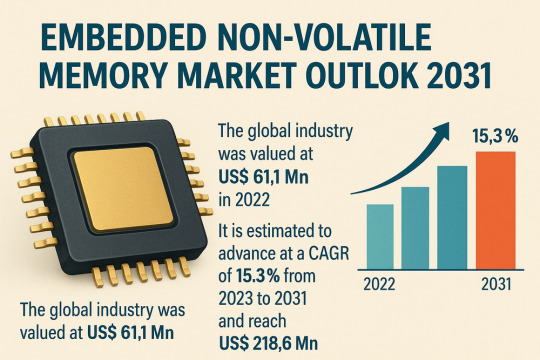
The global Embedded Non-volatile Memory (eNVM) market was valued at USD 61.1 million in 2022 and is projected to expand at a CAGR of 15.3% between 2023 and 2031, reaching USD 218.6 million by the end of 2031. Embedded NVM refers to non-volatile storage integrated directly into semiconductor chips, retaining data even when the system is powered off. Its core applications include firmware storage, calibration data retention, and secure configuration storage in microcontrollers, digital signal processors, and a wide array of embedded systems.
Market Drivers & Trends
Smartphone and Wearable Boom – The continued global uptake of mobile devices has escalated the need for larger, faster embedded memory. Users demand lightning-fast boot times and seamless multitasking, driving OEMs to integrate high-performance flash memory and emerging NVM technologies directly into system-on-chips (SoCs). – Wearables, smart speakers, and IoT gadgets prioritize low-density but highly efficient memory. 3D NAND flash has emerged as the preferred technology, offering high storage capacity in a minimal footprint. Samsung and SK Hynix have ramped up mass production of advanced 3D NAND modules tailored for connected device ecosystems.
Low-Power, High-Speed Requirements – Battery-powered devices mandate memory that combines rapid data access with minimal energy draw. Next-generation embedded NVMs—such as STT-MRAM and ReRAM—offer sub-microsecond access times and ultra-low standby currents, extending device lifespans and enhancing user experience. – System-in-Package (SiP) and Package-on-Package (PoP) solutions are gaining traction, integrating multiple memory dies and logic blocks into single compact modules, thereby reducing interconnect power losses and boosting overall throughput.
Security and Reliability – As embedded systems permeate mission-critical sectors (automotive ADAS, industrial controls, medical devices), secure and tamper-resistant memory is non-negotiable. Embedded flash and MRAM provide inherent read/write protections, while emerging PUF-based authentication schemes leverage intrinsic chip variability to safeguard cryptographic keys.
Latest Market Trends
3D XPoint and Beyond: Following its debut in enterprise SSDs, 3D XPoint is being miniaturized for embedded applications, promising DRAM-like speeds with non-volatility, ideal for real-time control systems.
Embedded MRAM/STT-MRAM: Gaining traction in safety-critical automotive and industrial sectors, MRAM offers unlimited endurance cycles and high radiation tolerance.
Embedded Ferroelectric RAM (FRAM): With nanosecond write speeds and high write endurance, FRAM is carving out niches in smart cards, metering, and medical devices.
Key Players and Industry Leaders The eNVM market is highly consolidated, with major semiconductor manufacturers and specialty memory providers driving innovation and capacity expansion:
eMemory Technology Inc.
Floadia Corporation
GlobalFoundries Inc.
Infineon Technologies AG
Japan Semiconductor Corporation
Kilopass Technology, Inc.
SK HYNIX INC.
SMIC
Texas Instruments Incorporated
Toshiba Electronic Devices & Storage Corporation
Download now to explore primary insights from our Report in this sample - https://www.transparencymarketresearch.com/sample/sample.php?flag=S&rep_id=24953
Recent Developments
March 2023 – ANAFLASH Commercialization U.S. startup ANAFLASH unveiled an energy-efficient embedded NVM solution tailored for battery-powered wireless sensors, medical wearables, and autonomous robots, promising up to 30% lower power consumption versus incumbent flash technologies.
February 2023 – GlobalFoundries Acquisition GlobalFoundries acquired Renesas Electronics’ resistive RAM patents and manufacturing know-how, aiming to integrate low-power ReRAM into next-generation SoCs for smart home and mobile applications.
May 2022 – Automotive Platform Collaboration Japan Semiconductor Corporation and Toshiba Electronic Devices partnered to develop a 0.13-micron analog IC platform with embedded flash, targeting advanced automotive applications such as in-vehicle networking and sensor fusion modules.
Market Opportunities
5G and IoT Rollout: The proliferation of 5G networks and edge computing devices demands local data storage and analytics, presenting growth avenues for low-latency embedded memory.
Automotive Electrification: Electric and autonomous vehicles require robust memory for ADAS, telematics, and battery management systems, creating new application segments.
Healthcare Wearables: Demand for continuous health monitoring fosters embedded memory integration in smart patches and implantable devices, where size and power constraints are paramount.
Future Outlook Analysts project that by 2031, the Embedded NVM market will surpass US$ 218 million, driven by sustained R&D investments and product diversification into emerging NVM technologies. The maturation of foundry support for STT-MRAM, ReRAM, and 3D XPoint, coupled with advanced packaging breakthroughs, will accelerate adoption across consumer, automotive, and industrial domains. Security-driven regulations and functional safety standards will further cement embedded memory’s role in next-generation electronic systems.
Market Segmentation
By Type
Flash Memory (dominant share in 2022)
EEPROM
nvSRAM
EPROM
3D NAND
MRAM/STT-MRAM
FRAM
Others (PCM, NRAM)
By End-Use Industry
Consumer Electronics (2022 market leader)
Automotive
IT & Telecommunication
Media & Entertainment
Aerospace & Defense
Others (Industrial, Healthcare)
By Region
North America
Europe
Asia Pacific (2022 market leader)
Middle East & Africa
South America
Buy this Premium Research Report for a detailed exploration of industry insights - https://www.transparencymarketresearch.com/checkout.php?rep_id=24953<ype=S
Regional Insights
Asia Pacific: Commanded the largest share in 2022, fueled by semiconductor R&D hubs in China, Japan, Taiwan, and South Korea, and robust electronics manufacturing ecosystems.
North America: Home to major foundries and design houses; 5G and IoT device adoption is expected to drive eNVM demand through 2031.
Europe: Automotive electrification and Industry 4.0 initiatives will underpin growth, with Germany and France leading demand.
MEA & Latin America: Emerging markets are gradually adopting consumer electronics and automotive technologies, presenting long-term opportunities.
Frequently Asked Questions
What is embedded non-volatile memory? Embedded NVM is memory integrated into semiconductor chips that retains data without power. It is used for firmware, configuration data, and security keys.
Which eNVM type holds the largest market share? Flash memory led the market in 2022 due to its balance of speed, density, and cost-effectiveness, particularly in consumer electronics and IoT devices.
What industries drive eNVM demand? Consumer electronics, automotive (ADAS, electrification), IT & telecom (5G equipment), aerospace & defense, healthcare wearables, and industrial automation.
How will emerging technologies impact the market? STT-MRAM, ReRAM, and 3D XPoint will offer faster speeds, higher endurance, and lower power profiles, expanding applications in safety-critical and high-performance systems.
Which regions offer the best growth prospects? Asia Pacific remains the leader due to manufacturing scale and R&D. North America and Europe follow, driven by advanced automotive and IoT deployments.
What factors may restrain market growth? High development costs for new NVM technologies, integration complexity, and supply chain disruptions in semiconductor fabrication could pose challenges.
Why is this report important for stakeholders? It equips semiconductor vendors, system integrators, and strategic investors with the insights needed to navigate technological shifts and seize emerging market opportunities in embedded memory.
Explore Latest Research Reports by Transparency Market Research:
Power Meter Market: https://www.transparencymarketresearch.com/power-meter-market.html
Radiation Hardened Electronics Market: https://www.transparencymarketresearch.com/radiation-hardened-electronics-semiconductor-market.html
AC-DC Power Supply Adapter Market: https://www.transparencymarketresearch.com/ac-dc-power-supply-adapter-market.html
5G PCB Market: https://www.transparencymarketresearch.com/5g-pcb-market.html
About Transparency Market Research Transparency Market Research, a global market research company registered at Wilmington, Delaware, United States, provides custom research and consulting services. Our exclusive blend of quantitative forecasting and trends analysis provides forward-looking insights for thousands of decision makers. Our experienced team of Analysts, Researchers, and Consultants use proprietary data sources and various tools & techniques to gather and analyses information. Our data repository is continuously updated and revised by a team of research experts, so that it always reflects the latest trends and information. With a broad research and analysis capability, Transparency Market Research employs rigorous primary and secondary research techniques in developing distinctive data sets and research material for business reports. Contact: Transparency Market Research Inc. CORPORATE HEADQUARTER DOWNTOWN, 1000 N. West Street, Suite 1200, Wilmington, Delaware 19801 USA Tel: +1-518-618-1030 USA - Canada Toll Free: 866-552-3453 Website: https://www.transparencymarketresearch.com Email: [email protected]
0 notes
Text
https://www.futureelectronics.com/p/semiconductors--microcontrollers--32-bit/stm32f205vct6-stmicroelectronics-4046841
Microcontroller 32 bit controller, 32-bit microcontroller programming
STM32F Series 512 kB Flash 128 kB RAM ARM Based 32-Bit Microcontroller -LQFP-100
#Microcontrollers#32 bit#STM32F205VCT6#STMicroelectronics#controller#32-bit microcontroller programming#USB#Embedded microcontrollers#microcontrollers software#Non-volatile memory#Low power microcontroller#wireless microcontroller
1 note
·
View note
Text
Flash Memory Market is Anticipated to Witness High Growth Owing to Rising Demand for High-Performance Storage
Flash memory is a non-volatile storage technology widely used in consumer electronics, data centers, automotive systems, and industrial applications. It stores data even when power is removed, delivering fast read/write speeds, energy efficiency, and compact form factors. The Flash Memory Market has expanded due to the proliferation of smartphones, solid-state drives (SSDs), and embedded systems, all requiring reliable and high-density storage solutions. Advantages such as low latency, durability, and scalability make flash memory ideal for handling intensive workloads in artificial intelligence, cloud computing, and the Internet of Things (IoT). Additionally, advancements in 3D NAND technology have boosted storage density while reducing cost per gigabyte, creating significant market growth opportunities.
Get More Insights on Flash Memory Market https://www.patreon.com/posts/flash-memory-is-128929607

#FlashMemoryMarket#FlashMemoryMarketTrends#NANDFlash#NORFlash#3DNANDTechnology#CoherentMarketInsights
0 notes
Text
Are You Ready? The Field Programmable Gate Array Market is Exploding!
Field Programmable Gate Array (FPGA) Industry Overview
The global Field Programmable Gate Arrays (FPGAs) Market was valued at $10.46 billion in 2022 and is projected to expand at an annual rate of 10.8% from 2023 to 2030. The increasing adoption of field programmable gate arrays in applications such as deep packet inspection, network processing, and security is expected to fuel their demand throughout the forecast period. The preference for FPGA architecture is growing due to its advantages, including low power consumption and high compute density. This trend is being driven by the rising need for efficient data flow and streaming data processing across various applications. For example, in February 2022, QuickLogic Corporation introduced PolarPro 3 to address the shortage of low-power FPGAs. This product is designed for ultra-low power consumption, making it ideal for wearables, handheld devices, and mobile applications. Such product launches by key industry players are anticipated to drive market growth over the forecast period.
Detailed Segmentation:
Type Insights
Mid-range FPGAs are expected to register the highest CAGR of 12.5% over the forecast period, owing to the properties offered by the segment such as low power consumption, small form factor, and high performance for FPGA-based devices. In addition, the advantages of the mid-range type segment that are capable of delivering a significant digital signal processing (DSP) along with embedded memory to logic ratio that enhances the intelligence for several applications is anticipated to drive the segment growth.
Application Insights
The military and aerospace segment is expected to expand at the fastest CAGR of 12.7% over the forecast period. Emergence of embedded field programmable gate array has particularly favored the aviation and defense industry by offering even better integration, reliability, and low power option over the traditional FPGAs, which is expected to drive the military and aerospace segment growth during the forecast period.
Technology Insights
Flash-based FPGAs are expected to register the fastest growth rate of 11.3% over the forecast period. The segment is witnessing high demand as major players upgrade their portfolios of FPGAs to cater to the growing demand from the expanding application base. Additionally, the rising trend favoring flash-based FPGAs over SRAM-based FPGAs due to their lower power consumption is also boosting the segment growth. The utilization of non-volatile flash memory for configuration storage eliminates the need for continuous power, aligning with the industry's emphasis on energy efficiency and power optimization. This power-saving feature is particularly advantageous in battery-powered devices, portable electronics, and energy-constrained applications, which is expected to drive the market growth over the forecast period.

Regional Insights
The South America region is expected to register a significant growth rate of 11.9% over the forecast period. This growth is attributed to the boost in the automobile, industrial, and aerospace sector, where the application of FPGA-based solutions is substantial, especially in Brazil. In addition, the growing demand for connectivity in the region is expected to augment the adoption of advanced telecommunications infrastructure along with the expansion of broadband networks, which is expected to drive the growth of the field programmable gate array market across the region.
Gather more insights about the market drivers, restraints, and growth of the Field Programmable Gate Array (FPGA) Market
Key Companies & Market Share Insights
The market is classified as highly competitive, with the presence of several field programmable gate array market players. The key players operating in the field programmable gate array industry are focusing on strategic alliances, mergers & acquisitions, expansion, and product development to remain competitive in the industry. For instance, in May 2023, Intel Corporation launched their new FPGAs, the Agilex 7 FPGAs with R-Tile. This product from the company is expected to be the first FPGA with CXL and PCIe 5.0 capabilities. Such developments are expected to propel the field programmable gate array market growth over the forecast period. Some of the major players in the global field programmable gate array (FPGA) market:
Intel Corporation
Xilinx, Inc.
Qualcomm Technologies, Inc.
NVIDIA Corporation
Broadcom
AMD, Inc.
Quicklogic Corporation
Lattice Semiconductor Corporation
Achronix Semiconductor Corporation
Microchip Technology Inc.
Order a free sample PDF of the Market Intelligence Study, published by Grand View Research.
0 notes
Text
Next Generation Memory Market Resilience and Risk Factors Impacting Growth to 2033
The Next-Generation Memory (NGM) market is undergoing a transformative phase, driven by the escalating demands of artificial intelligence (AI), Internet of Things (IoT), and data-intensive applications. These advanced memory technologies, including Magnetoresistive RAM (MRAM), Resistive RAM (ReRAM), Phase-Change RAM (PCRAM), and High Bandwidth Memory (HBM), are poised to redefine data storage and processing paradigms.
Key Technologies and Applications
High Bandwidth Memory (HBM): Advanced memory solutions like HBM3E and HBM4 are being developed to meet the high-speed data processing requirements of AI and machine learning applications. For instance, Nvidia has requested SK Hynix to expedite the supply of HBM4 chips to support its AI technology development.
MRAM and ReRAM: These non-volatile memory technologies offer high endurance and low power consumption, making them ideal for IoT devices and embedded systems. Their integration into these devices ensures reliable data storage and fast access speeds.
PCRAM: Utilized in applications requiring high-speed data access and low latency, such as in-memory computing and real-time data processing systems.
Download a Free Sample Report: - https://tinyurl.com/yshzhzxy
Market Drivers
AI and Machine Learning: The surge in AI applications necessitates memory solutions that can handle vast amounts of data with minimal latency. Next-generation memory technologies are tailored to meet these demands, offering high-speed data access and processing capabilities.
IoT Expansion: The proliferation of IoT devices generates enormous data volumes, requiring efficient and reliable memory solutions. NGM technologies like MRAM and ReRAM provide the necessary speed and endurance to support the growing IoT ecosystem.
Data Center Evolution: Modern data centers require memory solutions that balance speed, capacity, and energy efficiency. NGM technologies are being integrated into data centers to enhance performance and reduce energy consumption.
Challenges and Considerations
High Manufacturing Costs: The production of next-generation memory technologies involves complex processes and specialized materials, leading to higher manufacturing costs compared to traditional memory solutions.
Integration Complexities: Integrating NGM technologies into existing systems and infrastructure can be challenging, requiring significant investment in research and development and potential redesigns of hardware components.
Future Outlook
The next-generation memory market is poised for substantial growth, driven by technological advancements and the increasing demands of AI, IoT, and data-intensive applications. As companies continue to innovate and develop more efficient and cost-effective memory solutions, the adoption of NGM technologies is expected to accelerate across various industries.
Recent Industry Developments
Nvidia's Request to SK Hynix: Nvidia has asked SK Hynix to expedite the delivery of HBM4 chips by six months to support its AI technology development, highlighting the growing need for advanced memory solutions in AI applications.
Micron's Expansion Plans: Micron Technology is expanding its market share in high-bandwidth memory chips, with new R&D facilities in the U.S. and potential production in Malaysia, aiming to meet the increasing demand for advanced memory solutions.
Read Full Report: - https://www.uniprismmarketresearch.com/verticals/semiconductor-electronics/next-generation-memory
0 notes
Text
Top 5 Innovations in SAN Storage You Shouldn't Ignore in 2025
The Storage Area Network (SAN) landscape is primed for transformation in 2025. With rising data volumes, new security threats, and accelerating demands for high-performance access, SAN storage technology is evolving in ways that IT managers, tech enthusiasts, and business owners can’t afford to overlook. This blog explores the latest SAN storage innovations, outlines their real-world business impact, and provides guidance for integrating them into enterprise infrastructure.
A Changing SAN Storage Landscape
The modern enterprise depends on rapid, secure, and reliable access to massive amounts of data. SAN storage, already a mainstay of mission-critical environments, now faces new pressures:
Explosion of unstructured data from IoT and AI workloads
Increasing need for multi-site data resilience and business continuity
Tightening regulatory controls on data protection and privacy
Higher performance demands from real-time analytics and virtualization
Traditional SANs have delivered on performance and scale for years, but tomorrow’s requirements demand breakthroughs in speed, flexibility, and manageability. The following five innovations stand out as essential for any forward-looking organization planning its SAN storage roadmap in 2025.
1. NVMe over Fabrics (NVMe-oF): The Next-Generation Protocol
What is NVMe-oF?
Non-Volatile Memory Express over Fabrics (NVMe-oF) is revolutionizing SAN performance by allowing NVMe devices to communicate directly across network fabrics like Ethernet, Fibre Channel, or InfiniBand. Unlike legacy SCSI protocols, NVMe is end-to-end optimized for flash storage, dramatically lowering latency and boosting throughput.
Benefits and Implications
Ultra-low latency: NVMe-oF enables sub-100μs data access, critical for high-frequency trading, real-time analytics, and next-gen applications.
Massive bandwidth: Organizations can achieve multi-gigabit throughput, unlocking parallel data access on a scale previously reserved for hyperscale data centers.
Scalability: NVMe-oF scales seamlessly as workloads and device counts grow, supporting thousands of concurrent connections with uniform performance.
Real-World Applications
Financial institutions rely on NVMe-oF-powered SANs to execute trades in milliseconds. AI research labs benefit from rapid, concurrent access to massive datasets for model training and inference, while large healthcare providers accelerate access to critical medical imaging.
How to Prepare
Audit SAN infrastructure for NVMe-oF compatibility.
Plan phased upgrades from legacy Fibre Channel to NVMe-capable switches and adapters.
Consider hybrid deployments to balance cost and performance during transition.
2. AI-Driven Storage Optimization
What is AI for SAN Storage?
Artificial intelligence is moving beyond analytics, embedding itself in storage controllers to automate capacity management, performance tuning, and anomaly detection. By learning operational patterns, AI dynamically allocates resources, predicts failures, and even initiates remediation actions.
Benefits and Implications
Proactive health monitoring: AI models identify potential failures before they occur, minimizing unplanned downtime.
Self-optimizing SANs: Storage arrays adjust on the fly for fluctuating workloads, ensuring optimal performance at all times.
Resource efficiency: Automated tiering reduces manual intervention and maximizes hardware utilization.
Real-World Applications
Global retail chains use AI-driven SANs to ensure their e-commerce sites perform reliably throughout flash sales and holiday surges. Financial institutions maintain maximum uptime with predictive disk failure alerts and automated data migration.
How to Prepare
Evaluate current SAN vendors’ AI capabilities.
Enable telemetry and monitoring features that feed AI engines.
Train IT staff in interpreting AI-generated insights and automation controls.
3. Storage Class Memory (SCM) Integration
What is SCM?
Storage Class Memory bridges the gap between volatile DRAM and traditional NAND flash. With speeds closer to main memory but the persistence of storage, SCM technologies like Intel Optane transform application responsiveness and accelerate I/O-intensive workloads.
Benefits and Implications
Unmatched performance: SCM provides microsecond-level response times, ideal for in-memory databases, caching layers, and large-scale analytics.
Persistent memory: Critical data survives even during power loss, improving business continuity.
Reduced bottlenecks: Faster boot times and near-instant recovery enable new possibilities for always-on services.
Real-World Applications
Telecommunications companies deploy SCM to guarantee high-throughput, ultra-low-latency networks for real-time communications. E-commerce platforms use SCM as a cache to speed up order processing and transaction verification.
How to Prepare
Assess SAN controllers and server compatibility with SCM modules.
Identify candidate workloads that would benefit most from memory-speed storage.
Calculate cost-benefit thresholds, as SCM investments are typically higher per GB.
4. End-to-End Security Enhancements
What are the Latest SAN Security Innovations?
With heightened threats to data integrity and privacy, SAN vendors are embedding robust, end-to-end security directly into their infrastructure. Key innovations include encrypted traffic at rest and in motion, zero trust network architectures, and advanced key management integration.
Benefits and Implications
Data privacy compliance: Native encryption supports GDPR, HIPAA, and other regulatory frameworks.
Trustless access control: Zero trust models restrict lateral movement inside SANs, reducing exposure from internal threats.
Rapid breach response: Integrated auditing and automated anomaly detection accelerate incident response.
Real-World Applications
Healthcare institutions maintain HIPAA compliance with at-rest encryption and strict access controls. Enterprises with remote employees benefit from end-to-end encrypted sessions protecting intellectual property.
How to Prepare
Enforce encryption across all SAN nodes and data paths.
Implement multi-factor authentication and rigorous role-based access controls.
Regularly test backup/restore procedures in encrypted environments.
5. Multi-Cloud SAN Architectures
What is Multi-Cloud SAN?
To boost resilience and flexibility, enterprises are distributing SAN storage across on-premises facilities and multiple public clouds. Multi-cloud SAN enables unified management, burstable cloud capacity, and seamless disaster recovery, breaking the traditional data center boundaries.
Benefits and Implications
Business continuity: Replicate data across regions and providers, minimizing the risk of downtime or data loss.
Capacity on demand: Easily scale workloads up or down by leveraging cloud-native SAN storage.
Global performance: Serve data to remote offices and users without compromising speed or reliability.
Real-World Applications
Media production studios sync raw and edited footage between cloud and on-site SAN, enabling collaboration across continents. SaaS platforms leverage multi-cloud SAN to guarantee uptime and data sovereignty in different countries.
How to Prepare
Inventory data types and compliance needs to set cloud storage policies.
Integrate cloud gateways with on-premises SAN for unified management.
Test failover scenarios to validate disaster recovery readiness.
Strategies for SAN Storage Adoption in 2025
Transitioning to these advanced SAN features requires more than a hardware refresh. Here’s how forward-thinking IT teams can futureproof their storage:
Align technology with business priorities: Start with workloads that will derive the most benefit (e.g. real-time analytics, regulatory compliance, global collaboration).
Prioritize staff training: Ensure your team understands new protocols, AI dashboards, security policies, and multi-cloud integrations.
Adopt a phased rollout: Test innovations in controlled environments before scaling organization-wide.
Engage with trusted vendors: Work with suppliers offering proven solutions, transparent roadmaps, and robust support.
Shaping the Future of SAN Storage
Staying competitive means treating SAN storage solution as a dynamic asset, ready to evolve alongside your business needs. The innovations outlined above are not fads; they represent foundational shifts with lasting impact. Enterprises that adopt NVMe-oF, AI-driven optimization, SCM, advanced security, and multi-cloud architectures will achieve unprecedented levels of efficiency, agility, and security.
By proactively evaluating and integrating these advances, your organization can ensure it stands at the forefront of IT infrastructure excellence in 2025 and beyond.
0 notes
Text
A Comprehensive Guide to Firmware Development

In the world of embedded systems and smart devices, firmware plays a critical role in enabling hardware to function effectively. Whether you're developing IoT devices, automotive systems, or industrial machinery, firmware development is the backbone that bridges hardware and software.
In this blog post, we’ll explore what firmware is, its importance, the development process, tools used, and best practices to ensure efficient and secure firmware solutions.
What is Firmware?
Firmware is a specialized type of software that provides low-level control for a device's specific hardware. Unlike regular software applications, firmware is tightly coupled with the hardware and is often stored in non-volatile memory such as ROM, EEPROM, or flash memory.
Examples of devices with firmware include:
Smartphones
Routers
Smart TVs
Medical devices
Automotive control units (ECUs)
Why is Firmware Important?
Firmware is essential because it:
Controls hardware operations: Without firmware, the hardware components of a device would be non-functional.
Ensures device functionality: It manages startup routines, I/O operations, sensor integration, and communication protocols.
Supports software-hardware integration: Firmware acts as a middle layer, allowing high-level software applications to interact with low-level hardware components.
Enables updates: Firmware can often be updated to fix bugs, enhance performance, or add features.
The Firmware Development Process
1. Requirements Gathering
Understanding the hardware specifications and the device’s purpose is crucial. Developers need to gather requirements from both hardware engineers and end users.
2. Architecture Design
This involves deciding on the architecture and communication protocols (e.g., I2C, SPI, UART), memory usage, and timing constraints.
3. Choosing a Development Platform
Most firmware is written in C or C++ due to their efficiency and hardware-level access. You’ll also need:
Microcontroller/microprocessor datasheets
Board Support Packages (BSPs)
RTOS (Real-Time Operating System), if required
4. Coding and Integration
Firmware code is written to interface directly with hardware. This includes writing drivers for peripherals (LEDs, sensors, motors) and managing power consumption, timing, and interrupts.
5. Testing and Debugging
Testing includes:
Unit testing
Hardware-in-the-loop (HIL) testing
Simulation and emulation tools
Debugging tools such as JTAG and SWD are used to step through code and analyze performance.
6. Deployment
Once tested, firmware is compiled and flashed onto the device using programmers or over-the-air (OTA) update mechanisms.
Tools Used in Firmware Development
Integrated Development Environments (IDEs): Keil µVision, MPLAB X, STM32CubeIDE
Compilers and Toolchains: GCC, IAR Embedded Workbench
Debuggers/Programmers: JTAG, ST-LINK, AVR ISP
Version Control Systems: Git
Simulators/Emulators: QEMU, Proteus
Best Practices for Firmware Development
Write modular and reusable code
Follow coding standards (e.g., MISRA C for safety-critical systems)
Optimize for memory and power consumption
Document thoroughly for maintainability
Implement fail-safes and watchdog timers
Secure your firmware (e.g., with encryption and secure boot loaders)
Plan for firmware updates with mechanisms like OTA updates
0 notes
Link
[ad_1] Non-volatile memory is an important component in a wide range of high-performance embedded applications. Especially, many consumer, industrial, and medical applications need increased re-writability to support both more frequent code updates as well as increased data logging. These applications require greater memory density to store either a substantially larger code footprint and/or more extensive data logs. Moreover, developers need to be able to improve power efficiency while lowering system cost. Today, there are numerous non-volatile memory technologies available to developers, including EEPROM, NOR flash, NAND flash, MRAM, and FRAM. Each has its own distinct advantages for specific applications. However, the combination of 1) manufacturing process technologies continuing to scale smaller, 2) the need for higher densities at lower power, and 3) re-writability becoming increasing important has led to increased interest in RRAM for these applications. This article will explore RRAM technology and how it provides developers with a new approach to meeting the changing memory requirements of high-performance embedded systems. Memory in high-performance embedded systems Emerging connected systems face a number of tough design challenges. For instance, medical devices—such as hearing aids, continuous glucose monitors (CGMs), and patches—must fit into a smaller form factor despite increasing data and event logging requirements necessary to enable remote monitoring and compliance with industry standards. Next, smart equipment in Industry 4.0 systems require significantly greater code storage to facilitate functionality like remote sensing, edge processing, and firmware over-the-air (FOTA) updates for remote maintenance. Furthermore, the addition of artificial intelligence (AI) at the edge in wearables and Internet of Things (IoT) devices is driving the need for high-performance, energy-efficient non-volatile memory in smaller form factors. The increased code size and data logging requirements of such systems exceeds the embedded non-volatile memory capabilities of microcontrollers. External memory is needed to match increasing density and performance requirements. However, code and data often need varying capabilities depending upon performance, density, endurance, and data-write size. Thus, multiple non-volatile memories may have to be used, such as NOR flash for data logging and high-density EEPROM for code storage. This can lead to systems that use several types of external memory, increasing system cost, complexity, and energy consumption. Ideally, systems can use a single memory type that supports both external code and data storage without compromising performance or functionality for either. An emerging non-volatile technology to fill this gap as a standalone external memory is RRAM. Resistive RAM Resistive RAM (RRAM) is a non-volatile random-access memory that was made available commercially in the early 2000s. It operates by changing the resistance of a switching material sandwiched between two electrodes, show on left in Figure 1. Figure 1 Typical RRAM memory cell consists of one transistor and one resistor (left), and the memory state is altered by applying an external bias across the metal electrodes (right). Source: Infineon The switching material can be metal oxide or a conductive bridging switching media. A typical RRAM memory cell consists of one transistor and one resistor pair (1T1R) where the resistance of the RRAM can be altered with an external bias applied across the metal electrodes, shown on the right side of Figure 1. Initially, RRAM was developed as a potential replacement for flash memory. At the time, the cost and performance benefits of RRAM weren’t enough to supersede the advantages of other non-volatile memory technologies, especially as an external memory. However, in recent years, several factors have changed to make RRAM a compelling non-volatile alternative. Specifically, as embedded systems become more integrated and implemented in smaller manufacturing process nodes with substantially larger code and data storage requirements, the following advantages of RRAM for external memory overtake traditional non-volatile options: Scalability Some non-volatile memory technologies are limited in their ability to scale, translating to limitations in overall memory density due to footprint, power, and cost. A major advantage of RRAM is that it can be manufactured in a compatible CMOS process, enabling it to scale to process nodes below 45 nm and even down as low as 10 nm. For example, the memory industry has had difficulty cost-effectively scaling NOR flash memory as the technology seems to be physically limited to between 35 and 40 nm. Scalability has a direct impact on performance, density, footprint, and energy efficiency. Direct write Data storage for a NOR flash memory requires two operations: an erase operation to clear the target address followed by a write operation. The “direct write” functionality of RRAM eliminates the need to first erase memory. Thus, only a write operation is required to store data. Figure 2 shows the operations required for writing to both NOR flash and RRAM. Figure 2 NOR flash requires an erase operation before every write operation, increasing write time, energy consumption, and wear on memory cells. RRAM’s ability to direct write speeds write operations, conserves energy, and extends cell endurance. Source: Infineon This leads to much faster large-scale write operations for RRAM, such as during FOTA updates. Byte re-writeable Some non-volatile memories perform writes based on page size. For example, NOR flash page size is typically either 256 or 512 bytes. This means every write impacts the entire page. To change one byte, the page must be read and stored in a temporary buffer; the change is made to the temporary duplicate. The flash must then erase the page and write the entire page back in from the buffer. This process is time-consuming and wears the flash (typically 100k+ writes). In addition, data cells that are not changed are worn unnecessarily. Consequently, data logging with NOR flash requires that data is cached and then written in page-sized chunks, adding complexity and potential data loss during a power event. In contrast, RRAM write size is much smaller (few bytes) with higher endurance than NOR flash. This is more manageable and accommodates data logging requirements well since cells are worn only when written to. Thus, RRAM is robust and efficient for both code storage and data logging in the same memory device. Energy efficiency Through optimizations such as byte re-writability and eliminating erase operations during data writes, RRAM achieves better energy efficiency, up to 5x lower write energy and up to 8x lower read energy compared to traditional NOR flash. Radiation tolerance and electromagnetic immunity RRAM technology is inherently tolerant to radiation and electromagnetic interference (EMI). This makes RRAM an excellent choice for those applications where environmental robustness is essential. Consolidate code storage and data logging RRAM is a proven technology whose time has come. It’s an established technology that has been in embedded form in chips for over a decade as an internal non-volatile memory. With its ability to scale to smaller process nodes, provide higher endurance and re-writability at low power, and minimize write time and power consumption through direct write functionality, RRAM delivers high performance without compromising robustness or efficiency (Table 1). Table 1 The above data shows a comparison between RRAM and other non-volatile memory technologies. Source: Infineon RRAM is an ideal memory for consolidating both code storage and data logging in a single external memory to simplify design and reduce system complexity, making RRAM a compelling alternative to traditional non-volatile memories for many consumer, industrial, and medical applications. Bobby John is senior product marketing manager for memory solutions at Infineon Technologies. Related Content Resistive RAM Memory is Finally Here RRAM set to follow 3-D flash, says IMEC RRAM: A New Approach to Embedded Memory RRAM Startup Raises £7M to Support Data-Hungry Applications Monolithic embedded RRAM presents challenges, opportunities The post RRAM: Non-volatile memory for high-performance embedded applications appeared first on EDN. [ad_2] Source link
0 notes
Text
What are the key components of an embedded system?
Key Components of an Embedded System
An embedded system is a specialized computing system designed to perform dedicated tasks within a larger system. It is typically built to be highly efficient, reliable, and optimized for specific functions. Here are the key components of an embedded system:
1. Microcontroller/Microprocessor: The central unit of an embedded system, the microcontroller (or microprocessor), processes data and executes instructions. It typically includes a CPU, memory, and input/output interfaces, all integrated on a single chip. The microcontroller determines the system's speed, power consumption, and functionality.
2. Memory: Embedded systems often use different types of memory, such as ROM (Read-Only Memory) and RAM (Random Access Memory). ROM stores firmware and software, while RAM is used for temporary data storage during operations. Flash memory is also common, providing non-volatile storage for the system's data.
3. Sensors and Actuators: Sensors collect real-world data, such as temperature, pressure, or motion, while actuators convert signals into physical actions, like moving motors or turning on lights. These components allow embedded systems to interact with their environment and execute tasks based on input data.
4. Power Supply: Since embedded systems are often deployed in remote or portable environments, a reliable power supply is essential. Power management ensures that the system operates efficiently and can run on minimal power, extending battery life in portable applications.
5. Communication Interfaces: Embedded systems often require communication with other systems or networks. Communication interfaces such as UART, SPI, I2C, and Ethernet are used for data transfer between the embedded system and other devices.
6. Software/Firmware: The software or firmware controls the operation of the embedded system, instructing the hardware to perform specific tasks. It is usually optimized for performance and resource usage, ensuring the system works within its constraints.
To fully understand these components and their interaction, enrolling in an Embedded Systems Course can provide in-depth knowledge and hands-on experience in designing and programming embedded systems.
0 notes
Text
0 notes
Text
Complex Programmable Logic Devices (CPLDs) are vital components in the digital electronics ecosystem, offering customizable solutions for implementing logic functions. These integrated circuits stand out for their non-volatile memory, allowing them to retain configurations even when powered off, and their quick boot-up times. Unlike their counterparts, such as FPGAs, CPLDs are optimized for simpler logic applications, making them ideal for tasks like signal interfacing, control functions, and glue logic in embedded systems.
0 notes
Text
0 notes
Text
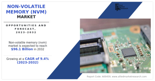
Non-Volatile Memory (NVM) Market Research Report for Complete Analysis of Current Scenario
Allied Market Research, titled, “Non-Volatile Memory (NVM) Market," The non-volatile memory (NVM) market size was valued at $41 billion in 2022, and is estimated to reach $96.1 billion by 2032, growing at a CAGR of 9.4% from 2023 to 2032.
The non-volatile memory (NVM) market growth is expected to exhibit moderate growth during the forecast period due to the increasing application of NVM in consumer electronic. Non-volatile memory is a type of secondary memory that stores the data permanently, even after a power outage. It employs user-configurable technology, which optimizes power consumption and enables faster access to the required data. In addition, NVM does not require periodic refreshment of the data as it is stored in a particular location. Non-volatile memory particularly creates a backup of the information and prevents data loss.
It is electrically programmable and erasable, to store changes in a particular location within the storage device. The increase in the demand for advanced automated applications allows the end user to switch to embedded non-volatile memory from traditional memory. Moreover, the market growth is further supported by its unmatched benefits such as, enhanced storage space, higher security of data, and improved scalable memory through various addressing types, such as electrically addressed, mechanically addressed, and others. Presently, low endurance and lower storage density in NVM are observed as major restraints for growth. However, these restraints are expected to lose their impact soon, owing to the increase in acceptance of non-volatile memory in consumer electronics.
Among the types covered under the scope of the report, the electrically addressed Non-volatile memory type held the largest market share in 2022 and is expected to grow at a significant CAGR over the forecast period. Emerging memory such as 3D XPoint, MRAM, SONOS, NRAM swiftly gains popularity among enterprises as these offer high endurance and bigger storage density. It is expected to exhibit significant growth during the forecast period.
Based on mechanically addressed type, hard-disk drive is presently the highest revenue generating segment, as it is increasingly being used among enterprises. The millipede memory segment is anticipated to be the most lucrative non-volatile memory (NVM) market share providers. It utilizes local probe techniques to read, write, backup and erase the data and offers ultrahigh average storage density of 1 Tbit/in 2. Among various applications, enterprise storage is the predominant segment in 2022. The growth of enterprise segment is primarily driven by the rapidly widening enterprise storage and server systems, which further necessitates the greater demand for non-volatile memory.
By industry vertical, non-volatile memory is segmented into telecom & IT, healthcare, transportation, energy & power, manufacturing industries, and others. Telecom and IT contributed the highest revenue in 2022, as it is used in data centers to store the data permanently. However, automotive is expected to attain the highest CAGR during the forecast period, owing to the increase in demand for advanced automotive applications.
The global Non-Volatile Memory (NVM) Market Analysis is analyzed on the basis of region across North America, Europe, Asia-Pacific, and LAMEA. The Asia-Pacific market is the predominant region and is expected to generate the largest share in 2022, due to an increase in advanced consumer electronic products and huge investment by companies in the automotive industry for automated applications. Asia-Pacific is estimated to be the fastest growing region the forecast period, owing to rapid demands in semiconductor industry and a demand for memories in countries such as China, Singapore, and Japan.
KEY FINDINGS OF THE STUDY
The non-volatile memory (NVM) industry is expected to continue growing in the coming years, driven by increasing demand for laminated products across various industries, technological advancements, and a growing trend towards sustainability.
The growing non-volatile memory (NVM) market trends towards sustainability is driving the adoption of eco-friendly materials in the production of non-volatile memory products. Scanners that use sustainable materials and processes are in high demand, and manufacturers are investing in the development of environmentally friendly non-volatile memory.
Asia Pacific is the largest market for non-volatile memory chip, driven by the increasing demand for non-volatile memory products in industries such as packaging, building materials, and automotive. The region is also home to some of the largest manufacturers of scanners.
The non-volatile memory market is highly competitive, with several major players operating globally. To remain competitive, companies are focusing on product innovation, strategic partnerships, and expanding their distribution networks.
The key non-volatile memory market leaders profiled in the report include Micron Technology Inc., Samsung Electronics Co Ltd, Intel Corporation, KIOXIA Holdings Corporation, Western Digital Corporation, Viking Technology, SK HYNIX INC., Renesas Electronics, STMicroelectronics N.V., and Fujitsu Limited. These key players adopt several strategies such as new product launch and development, acquisition, partnership and collaboration and business expansion to increase the Non-volatile memory market share during the forecast period.
0 notes
Text
Next-Generation Memory: Shaping the Future of Data Storage
Next-generation memory technologies are transforming data storage by offering enhanced performance, capacity, and energy efficiency compared to traditional memory solutions. Innovations in this field include advancements in non-volatile memory (NVM) technologies such as 3D NAND flash, phase-change memory (PCM), and resistive random-access memory (ReRAM). These technologies address the growing demand for faster data access, increased storage density, and lower power consumption in a variety of applications, from consumer electronics to enterprise data centers. The development of next-generation memory is crucial for supporting emerging technologies like artificial intelligence (AI), big data analytics, and the Internet of Things (IoT).
The Next-Generation Memory Market, valued at USD 6.3 billion in 2022, is projected to reach USD 33.65 billion by 2030, with a CAGR of 23.3% from 2023 to 2030.
Future Scope:
The future of next-generation memory will be driven by ongoing research and development in memory technologies and their integration into new applications. Key areas of focus will include increasing memory density, improving read/write speeds, and enhancing energy efficiency. Innovations such as 3D memory stacking and hybrid memory architectures will enable the development of more powerful and compact memory solutions. The proliferation of AI, IoT, and 5G technologies will further accelerate the demand for advanced memory solutions capable of handling large volumes of data and delivering high-speed performance.
Key Points:
Next-generation memory technologies offer improvements in performance, capacity, and energy efficiency.
Innovations include 3D NAND flash, phase-change memory (PCM), and resistive random-access memory (ReRAM).
Future developments will focus on increasing memory density, speed, and efficiency.
Trends:
Key trends in the next-generation memory market include the increasing adoption of 3D NAND flash technology, which provides higher storage densities and improved performance compared to traditional 2D NAND. The rise of AI and big data applications is driving demand for faster and more efficient memory solutions, leading to the development of advanced NVM technologies. Hybrid memory systems, which combine different types of memory technologies, are gaining traction for their ability to optimize performance and cost. Additionally, research into new memory materials and architectures is advancing the capabilities of next-generation memory.
Application:
Next-generation memory technologies are used in a variety of applications, including consumer electronics (smartphones, tablets, and laptops), enterprise storage systems (data centers and cloud computing), and embedded systems (automotive and industrial applications). They play a crucial role in enhancing data access speeds, increasing storage capacities, and reducing power consumption. The technology is also vital for emerging applications such as AI, IoT, and advanced analytics, where high-performance memory is essential for processing large volumes of data.
Conclusion:
Next-generation memory technologies are pivotal in advancing data storage solutions by offering significant improvements in performance, capacity, and energy efficiency. As technology continues to evolve, innovations in memory materials, architectures, and integration will drive further advancements. The growing demands of AI, IoT, and big data will ensure that next-generation memory remains at the forefront of technological development, supporting the creation of faster, more efficient, and high-capacity data storage solutions.
Read More Details: https://www.snsinsider.com/reports/next-generation-memory-market-4086
About Us:
SNS Insider is one of the leading market research and consulting agencies that dominates the market research industry globally. Our company’s aim is to give clients the knowledge they require in order to function in changing circumstances. In order to give you current, accurate market data, consumer insights, and opinions so that you can make decisions with confidence, we employ a variety of techniques, including surveys, video talks, and focus groups around the world.
Contact Us:
Akash Anand — Head of Business Development & Strategy
Email: [email protected]
Phone: +1–415–230–0044 (US) | +91–7798602273 (IND)
0 notes