#Gate preprations
Explore tagged Tumblr posts
Visit Tumblr Blog
Explore Tumblr blogs with no restrictions, modern design and the best experience.
Last Seen Tumblr Blogs


Fun Fact
Tumblr has a low social media market share in South America.
Text
GATE 2026 COURSES Get Ready with Engineers Institute of India

GATE 2026 is your ticket to top M.Tech programs and PSU jobs. If you're serious about cracking the exam, the right guidance can make all the difference. Engineers Institute of India (EII) is here to help with expert coaching, structured study plans, and a variety of learning options to suit your needs.
Why Choose Engineers Institute of India for GATE 2026?
Learn from the Best 🔗 Stay Updated & Register Here: https://forms.gle/5WVzPLU5HSZExDc58
Our experienced faculty members have years of expertise in GATE coaching. They simplify complex concepts, provide shortcut techniques, and ensure you’re well-prepared to tackle any question.
Study the Way That Works for You
We understand that every student has a different learning style, so we offer multiple study modes:
Live Online Classes + Backups – Attend interactive classes from anywhere and access recorded sessions for revision.
Offline Classroom Coaching – Get in-depth learning with direct faculty interaction in a structured classroom setup.
Recorded Video Lectures – Learn at your own pace with high-quality subject-wise video lectures.
Postal Study Materials (DLP) – Receive well-structured notes that make self-study easier and more effective.
All India Online Test Series – Attempt mock tests designed to match the latest GATE pattern and evaluate your performance.
Short-Term Crash Course – Ideal for students looking for quick revision and concept reinforcement.
Up-to-Date Study Material
Our study resources are carefully curated and regularly updated to match the latest GATE syllabus and exam trends, ensuring you study only what's relevant.
Mock Tests & Performance Tracking
With EII’s All India Online Test Series and regular assessments, you get a real-time exam experience, helping you identify strengths and work on weaker areas.
GATE 2026 Courses Offered
EII provides specialized coaching in the following engineering disciplines:
Chemical Engineering
Computer Science & IT
Civil Engineering
Mechanical Engineering
Electrical & Electronics Engineering
Our structured courses cover everything from the basics to advanced concepts, making sure you’re fully prepared.
Start Your GATE 2026 Preparation Now!
Success in GATE requires the right strategy and expert guidance. Choose the best learning mode for you and take a step closer to achieving your dream score.
📍 For More Information: Engineers Institute of India
Contact Us
📍 Engineers Institute of India (EII) Address: 61C, Kalu-Sarai near GATE No.4, Hauz Khas Metro-Station, New Delhi - 110016 📞 Phone: 9718856466 / 9990657855 📧 Email: [email protected]
Join Engineers Institute of India and start your journey towards GATE 2026 success today!
0 notes
Link
Here a few tips for gate 2020 preparation that will help your exam
0 notes
Text
Nikki Yadav Wiki, Murder Case Update, Family, Boyfriend, Age, Biography, Height, Instagram

Nikki Yadav Wiki:- Nikki Yadav was a 22 years old Indian girl who was killed by her 24-year-old boyfriend on 9 February 2023. Her boyfriend Sahil Gehlot strangled her throat via a mobile cable in the car and kept her dead boy in the fridge of his dhaba. Police were told by someone about her dead body and police recovered the dead body on 10 February 2023. Sahil Gehlot was arrested on 14 February 2023. In this article, you can get all the details about Nikki Yadav Wiki, Murder Case Update, Family, Boyfriend, Age, Biography, Height, and Instagram.
Nikki Yadav Wiki
Nikki Yadav was born in Khedi Khummar Village, Jhajjar, Haryana in 2001. She was 22 years old when she was killed. She completed her high school study in Jhajjar. She moved to Uttam Nagar, South Delhi to prepare for the Medical Entrance Exam at Aakash Institute in Uttam Nagar. Later she joined BA in English honors in the D. Pharma at Galgotia College.
Nikki Yadav Murder Case Update
Nikki's boyfriend Sahil Gehlot's marriage was fixed by his family elsewhere. His marriage was on 10 February 2023. When Nikki knew about his wedding on 9 February 2023 then he called her to meet and planned to go to Goa but he canceled the plan in the evening when they were in the car. They had a fight in the car over marriage and things got so bad that Sahil strangled her throat with the mobile charger's cable a the ISBT located at Kashemere Gate. She died. He reached Mitraon village, 35 km away where he has his own dhaba. He kept her dead body in the fridge of his dhaba and he moved to his house. Police were told by someone about her dead body and police recovered the dead body on 10 February 2023.
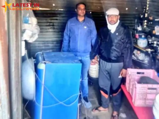
Sahil Gehlot hid Nikki's dead body in fridge Police arrested Sahil Gehlot on 14 February 2023 on Tuesday and the court sent him on remand for 5 days. Nikki's body was sent to Deen Dayal Upadhyay Hospital for postmortem.
Nikki Yadav Biography, Age, Wiki, Family
Nikki Yadav Wiki Name Nikki Yadav Birthplace Khedi Khummar Village, Jhajjar, Haryana Date of Birth 2001 Age 22 Years Old Parents Sunil Dutt (Father) and Mrs. Dutt (Mother) Religion Hinduism School Local Private High School in Khedi Khummar Village College Galgotia College Post Category Wiki
Nikki Yadav Family (Father and Mother)
Nikki Yadav was born to Sunil Dutt (Father) and Mrs. Dutt (Mother). Her family lives in Khedi Khummar village in Jhajjar, Haryana. She is the niece of Jawan Praveen Yadav.

Nikki Yadav's Father Praveen was involved in the 1999 Operation Vijay in Kargil War who lost both his hands in the war. His right leg doesn't work properly. Nikki's father told that they have network issues in village Khummar that's why people have to go to the terrace to talk on the phone. When Sunil Dutt didn't call for many days from his daughter, he thought that the phone was not ringing due to network failure. But later they got worried and he reached Delhi to get Nikki's address and went to Sahil's house to inquire about Nikki. Sahil's relatives assured him that Sahil would bring her back. Sunil got the news of his daughter's death and her family left for Delhi.
Nikki Yadav Boyfriend
Nikki Yadav was an unmarried girl who met Sahil Gehlot in Delhi. Sahil is 24 years old from Mitraon Village of Najafgarh. They met in coaching in 2018 when after Sahil came to Delhi in January 2018 for preparing for the SSC exam at Career Point Coaching in Uttam Nagr. At that time, Nikki started preprations for the Medical Entrance Exam at Aakash Insititue in Uttam Nagar. They used to go and come in the same bus so they became firends and fell in love. Later Sahil joined Galgotia College, Greater Noida in February 2018 to study D. Pharma and Nikki joined BA in the same colelge. They started to living together in a rented house in Greater Noida. Sahil got married to a gril from Bahadurgarh in Haryan on 10 Febraury 2023.

Nikki Yadav With Her Boyfriend Sahil Gehlot
Nikki Yadav Height, Weight
Nikki Yadav was 5 feet 6 inches tall. Her weight was around 65 kg.
Nikki Yadav Instagram
Nikki Yadav's Instagram is not revealed yet.
FAQs About Nikki Yadav Wiki
Q.1 Who was Nikki Yadav? Ans. Nikki Yadav was a 22 years old Indian girl who was killed by her 24-year-old boyfriend on 9 February 2023. Q.2 How old was Nikki Yadav? Ans. 22 Years Old Q.3 Who are Nikki Yadav's parents? Ans. Sunil Dutt (Father) and Mrs. Dutt (Mother) Q.4 Who was Nikki Yadav's boyfriend? Ans. Sahil Gehlot Q.5 What was Nikki Yadav's height? Ans. Around 5 Feet 6 Inches. Read Also: Nikki Yadav Murder Case Update Read the full article
#NikkiYadavAge#NikkiYadavBiography#NikkiYadavBoyfriend#NikkiYadavFamily#NikkiYadavHeight#NikkiYadavInstagram#NikkiYadavMurderCaseUpdate#NikkiYadavWiki
0 notes
Text
What is the Best Strategy to Prepare EDC for GATE Exam?
Hi guys today I’ll be sharing my strategy for how to prepare for Electronic Devices and Circuits for GATE . It’s one of the easiest subject from GATE point of view the only hard part is to memorize all the formulae from various topics apart from that it’s the least time consuming subject in respect to the weightage it shows in GATE exam preparation . EDC cousrse basically provides you with understanding of device physics which also forms a base for various circuit analysis and design courses.
In recent year level of question as well as the weightage of EDC in GATE exam has increased,from last 4 year anlaysis the minimum weightage seen for this subject was 6 and maximum was 12 in 2018 and 2017 it was one of the highest weighted subject and most of the toppers scored full marks in this subject .
Good knowledege of this subject can also help you after GATE in interviews of various IIT’s and PSU .If someone is looking forward to do specialization in Microelectronics this is one of the core subjects of this field ,where you will further learn in depth about device physics and after masters you can start your carrer as device engineer , a good device engineer are very higly paid.
GATE SYLLABUS
Here I have mentioned the GATE syllabus and i have divide it in parts and in next section i’ll pick out each part and discuss what to prepare and important topics for GATE
Semiconductor Physics:
Energy bands in intrinsic and extrinsic silicon, Carrier transport: diffusion current, drift current, mobility and resistivity, Generation and recombination of carriers ,Poisson and continuity equations.
Diodes
P-N junction, Zener diode.
Transistors
BJT, MOS capacitor, MOSFET .
Photovoltaic devices
LED, photo diode and solar cell .
Integrated circuit fabrication process:
oxidation, diffusion, ion implantation, photolithography and twin-tub CMOS process.
SYLLABUS DESCRIPTION AND PREPRATION STRATERGY
I would recommend you to give around 10 to 13 days for EDC in which you’ll have to cover theory, previous year GATE paper questions and solve some extra material for question practice . First of all, before starting this topic all of you should have basic idea about semiconductor, metals, and insulators, how are they classified, band model and bond model, direct and indirect band gap materials.
1). SEMICONDUCTOR PHYSICS (2-3 days)
This topic is some what between easy and moderate level ,but very important as it forms the basics for your further topics . Most of the parts are easy but few parts which are tricky and from which you can expect good level of questions are ��
Enerdy band digram.
Carrier transport.
Graded impurity distribution.
Carrier generation and recombination.
This topic deals with semiconductor physics(particularly silicon) basically to study about properties of the semiconductor.
Silicon crystal structure ,no of valence electron ,Energy band gap etc. Graph related question can be sometime tricky so one should have good understanding of theory to answer those.
In intrinsic semiconductor study about its eletrical property like conductivity and it’s variation with temperature then mobility variation with temperature , velocity saturation at high electric field and understand graph of µ vs T and σ vs T Vd (drift velocity)vs E.
Then calculation position of intrinsic fermi level , calculation of electrons n and hole concentration p ,calculation of intrinsic concentration,mass action law ,charge neutrality, graph of ni vs T and ln(σ ) vs 1/T Once your’e done with intrinsic semiconductor Physic slightly modifies for extrinsic semicoductor calculation ,extra parts that you should know is compensated doping , non degenartive and degenerative semiconductor,variation in nature of semiconductor with temperature.
in carrier transport you should learn about drift and diffusion current density and their expression for n type and p type ,diffusion constant and mobility, life time of carrier, diffusion length ,Einstein relation.
Graded impurity distribution is very important topic in this you shoul learn about non uniform doping ,relation between doping profile and Electric field ,plot of electric field for different doping profile ,current density at equilibrium,good level numerical and graphical question can be framed from it.
Hall effect mechanism , hall coefficient for n type p type and intrinsic semiconductor,hall voltage and it’s application are important, formula based question can be asked from this.
Enerdy band digram is one of the most important and hard topic in EDC if you don’t understand it future topics can be really difficult for you as it forms the base for understanding other devices ,you should learn variation of energy band with applied voltage ,calculation of electric field from slope of band digram and fermi level variation for equilibrium case (also for non -equilibrium but not in detail).
In Carrier generation and recombination process you should learn about phonon(thermal) geneneration and photo(light) generation, expression for excess charge carrier due to light excitation and net recombination rate at steady state.
Poisson and continuity equation is same as in EMT you should learn about Minority carrier continuity equation this equation helps you to sove various problem on steady state injenction in semiconductor due to different excitation.
After learning this topics you can easily analyze physics of any device .
2). Diodes (2 days)
In diode Band Digrams can be difficulty to understand and calculation of Diode parameter like depletion width ,junction potential.
As a pre requisite you should have a good understanding of electrostatic which you can cover from EMT.
In GATE most question are asked from Step graded pn junction so you should know how to plot charge density profile for step graded pn juction and to derive plot for Electric field from it and Potential plot from Electric field and your Energy band diagram is just an inversion of your potential plot.
Charge density →Electric field →Potential plot →Energy band diagram
you should should be very clear about how to draw plot for all these not only for step graded but for any profile and to derive the above parameter.
In last few years many questions are asked from Juction law in diode and flow of charge carrier through drift and diffusion which can confuse you
Diode capcitance in reverse and forward bais for abrupt and linear junction are also important and break down mechanism in diode and there relation with doping concentration and temperature.
Transient in diode can be a hard part some time syou can expect good question from diode switching.
You should also give some time to schottky diode ,One sided pn junction and understand metal semiconductor junction this helps you to study MOS capcacitor
3).Transistor ( 3 days )
BJT (half day)
This is very small and easy topic in EDC as most of the theory you cover in Anlaog circuits some extra things that you might find difficult can be Band digrams in equilibrium and diiferent baising region.
You should study Early effect and it effect on various parameter and punch through then you should cover breakdown in BJT in different junction and relation between breakdown Vceo and Vcbo.
You should also cover topic like minority carrier distribution in different operating region , BJT time delay factor and its cut off frequency, Ebers Moll model.
MOS CAPACITOR(2 days)
This is one of the most important topic in EDC it’s basically like studying OPAM in Analog ckt. This topics will require time to understand and many tricky questionss can be asked from this topic . Most of the students finds it very difficult to learn. First you should start with basic working of MOS capacitor in all three regime accumulation , depletion, and inversion and then you should study it’s band diagram in all the three region then you should start with C-V curve of MOS in this you should know the concept of surface potential , flat band voltage and threshold voltage. For studying flatband voltage Vfb you should understand the concept of workfunction for metal and semiconductor then you should study about trapped oxide charges and finally the complete expression for Vfb in term of bothFor threshold voltage Vt you should study the expression for depletion charge , surface potential at Vt. Depletion width in the semiconductor is calculated by doing one sided pn juction calculation. You should also study the calculation of inversion layer charge density. Then you should learn expression for capacitance in a different region (Cox , Cdep and Cinv) and in the inversion region, you should analyze both LFCV and HFCV curve. Finally you should study fixed oxide and interface traps charge and their effect on the C-V curve.
MOSFET (half day )
Again most of the MOSFET theory you cover in analog but prior to MOSFET, you study MOS capacitor which forms the base for MOSFET .
You should study various short channel effect in MOSFET which cause variation in its parameter and you should study variation in threshold voltage with variation in a parameter like length , oxide thickness , substrate doping etc.
You should study all the operating region of MOSFET and solve a problem related to finding operation region of different MOSFET in ckt and graph as well the expression of gm with respect to Vgs , Id .
4) PHOTOVOLTAIC DEVICES (1 DAY)
LED
very easy and can be covered in no time, you should study about direct bandgap semiconductor and reaction between Eg and λ relation between material bandgap and cut in voltage and parameter like extraction efficiency , internal radiative efficiency and external efficiency.
PHOTODIODE
In this you should learn about it’s working , operation region and parameter like photo current, dark current, Respositivity and expression for sensitivity and quantum effiency
SOLAR CELL
It’s is the most important photovoltaic device with respect to GATE and can be some times hard for some students to learn , you learn it’s working and it’s I-V graph basically there are 4 parameter you should know Voc, Isc, Conversion efficiency and fill factor.
5)Integrated circuit fabrication process(half day)
these topics are very easy but most students don’t find proper material to study these topic .
oxidation – study about wet and dry oxidation basically how much temprature is required and quality of oxide produce
diffusion and ion implantation- both are used for the same purpose but study what is their specific application and temperature require to perform both and concept of annealing
photolithography – In this you should cover topic likemasking, Photoresist , etching.
twin-tub CMOS process – you should study all the steps required and in order for fabriaction.
This topic might come for one marks you can refer any device book for these process.
BOOKS TO BE USED
1). SEMICONDUCTOR PHYSICS and DEVICES 4e – DONALD A NEAMEN
DHRUBES BISWAS
This book is one of the best book for EDC it’s little hard to understand but once you’ll study this completely I can assure you that you won’t be losing any marks in EDC it cover every topic except fabrication process,many of it’s excersice question are directly given in GATE exam one should definetly refer this book for good understanding of EDC . DIODE, TRANSISTOR, PHOTOVOLTAIC DEVICES can be directly referred from this book GATE related every aspect is covered.
2). SOLID STATE ELECTRONIC DEVICES – BEN G STREETMAN
This book is also a really good book some what easier to understand and cover most of the syllabus for EDC in the gate.
REFERENCE MATERIAL: for refrence, you can use nptel , PDF are availabel for devices courses with really good content
1 note
·
View note
Text
WHAT IS THE ENGINNERING MECHANICS? AND WHAT IS THE SYLLABUS? (PART 1) (GATE PREPRATION)
https://www.mechstech.com/2021/05/what-is-enginnering-mechanics-and-what.html
0 notes
Link
Join Our Institute providing Best GATE Coaching In Chandigarh. We have 10 Years of Experienced GATE Qualified Permanent Faculties From IIT and Online Free Mock Test after Prepration For More Info Call +919915314779 . #BioTechSapiens

0 notes
Text
My first post
Hi ,
I am Gate aspirant , preparing for GATE exam conducted by IIT
its my childhood dream to get into one of the most prestigious institute in India .
and Gate is the gate way to that so I am working hard for that ,
I have created this to track my progress on preparation of exam
0 notes
Photo

BAD MEDICINE ~Infectious teachers~ [PC GAME] Kuzuha Kakeru (History) Route Translations (Part 14)
MC’s name is retained as the original MC name Kawana Hina.
* Words within ‘ ‘ are spoken in English – *Spoiler free : Translations under cut! * Will update actual image of part one once I get on my main laptop
Part 1 / Part 2 / Part 3 / Part 4 / Part 5 / Part 6 / Part 7 / Part 8 / Part 9 / Part 10 / Part 11 / Part 12 / Part 13/ Part 14 Ruin END Prologue / Ruin END / True END
Hina:
(The world history prepration room……the lights there are on. I haven’t thought up of any good ideas but I think I’ll just tell him straight about what I think!)
--Please excuse me.
Kuzuha:
What’s the matter today?Do you have a question?
Hina:
……Um……there’s something I’d like to ask of you.
Kuzuha:
Feel free to ask about anythi~ng.
Hina:
Is it true that you’re going to quit the schol?
Kuzuha:
…………
Tch, it must be Remu.
Saying unnecessary things……
Hina:
Sensei……
Kuzuha:
Ah-……Well, I wonder about that.
Anyway, if it isn't about world history then I'm sorry but could we do this another time?
Hina:
Please don't avoid the topic.
Kuzuha:
Oi oi, there's no way I'd avoid a questions from a cute student is there?
However, this is something regarding my personal matters.
I don't have to tell you, a student, about everything.
……Well……
If you want to know no matter what……
How about having that kind of a relationship with me at your own risk of getting expelled from school?
……Nn……
Hina:
I-I don't have any intention of doing that!
Kuzuha:
……If so then hurry and leave.
Hina:
Please wait……
Please, let’s just talk a little at the very least……!
Kuzuha:
Even without you saying that, I've been asked left and right if I was really gonna get married today so I'm really fed up.
Hina:
But……I……
Just wanted you to……
Hear out what I have to say……!
(What should I do, my tears……)
Kuzuha:
…………Haa……
……Right, I have to hear out what you have to say, right?
I won't do mean things anymore so don't cry. Okay?
Hina:
Sen...sei……?
Um……
Kuzuha:
So, what was it that you wanted me to hear?
Hina:
I……regarding your marriage……
I just want you to think more seriously about it……
Kuzuha:
Haa……that again huh.
So what after I think about it?
Would you rather I quit the marriage and become yours?
Could it be that you love me?
Hina:
T-That’s not what I meant……!
I was just saying that I think it'd be better if you gave up the marriage……!
Kuzuha:
Give up……give up huh
That's right.
People like you……
Are one's who gets rid of things if things doesn't go your way.
Hina:
Eh……?
Kuzuha:
Being patted on the head……getting spoiled……
Being unable to be satisfied until you're more special compared to everyone else.
Hina:
Why are you saying things like this……?
Kuzuha:
Why?Let me tell you about it, if you're going to ask that. Specially so……
I--
Kuzuha’s Father:
You were with another guy again……!
Kuzuha’s Mother:
So what if I was!?
It's your……it’s your fault!
Because you've never made me satisfied!
Wealth, body, everything, everything……!!
Uuu……UUUUUUUu!!
Kuzuha:
…………
Kuzuha’s Father
Oi, who is it that brought a kid to a place like this!
Maid:
I-I deeply apologize!
--Let’s go, Kakeru-sama
Kuzuha:
O-Okay……
Maid:
Here, young master. Please have your dinner.
Kuzuha:
……Hey, where's mommy and daddy?
Are they fighting again?
Uuu……hic, hic……
I want to eat together with everyone. Why can't I do thay……?
Maid:
……Young master……
Please don't cry.
It's alright, it'll be fine……
……I……no, you have me don't you?
……Nn……
It’s fine if you raise your voice…...Especially for me……
Hina:
(To think that something like that had happened……)
Kuzuha:
Kukuku……Woman?Marraige?
Ahhh, really, how boring it is--
In the end, everything……will end up the same as that no matter what.
You've already understood, haven't you?
I don't see marriage as something as dreamlike as you imagine it to be.
You know……don’t tell others about it?
Because I only told you as an exception, okay?
Don't tell anyone else.
Right……it’ll be a secret between only the two of us.
Women will be pleased if I say such things, right?
Are you happy too?To be something special to me?
Woman are really worthless creatures.
Though I also feel like shit, having to marry something like that.
Hina:
(Kuzuha-sensei……)
What should I do?
Choice A: Go to the Infirmary Choice B: Go to the front of the school gate
#Bad Medicine Infectious Teachers#Bad Medicine Infectious Teachers Game#Kuzuha Kakeru#Shido Kaname#Yanagi Ryota#Tojo Kairi#Nagihara Taiki#Kashu Remu#Rejet#Otome#Translations
5 notes
·
View notes
Text
Mesmerizing Taste from Famous Restaurant in Udaipur Bawarchi Restaurant
Mesmerizing Taste from Famous Restaurant in Udaipur Bawarchi Restaurant http://www.bawarchirestaurant.in/
Bawarchi Restaurant is famous for its ambience and taste of food. We are located at Delhi gate which is near to all the major areas of Udaipur, so it’s really very easy to reach Bawarchi. Now a day’s everyone is searching for pure food which is hundred percent made up of fresh vegetable and pure ghee,masalas. Bawarchi fulfill your this demand as we use best masalas and fresh vegetables.

Mesmerizing Taste from Famous Restaurant in Udaipur Bawarchi Restaurant http://www.bawarchirestaurant.in/
Bawarchi has its own secret recipe for food prepration, which gives prepared food an extra flavor and good test. We also offer many types of food Thalis like Rajasthani Thali, Gujarati Thali, and Jain Thali. If you want to enjoy real taste of Rajasthani food, you should visit Bawarchi. Bawarchi is famous and well known all around Udaipur.
Mesmerizing Taste from Famous Restaurant in Udaipur Bawarchi Restaurant http://www.bawarchirestaurant.in/
Daal Makhani and Matar Paneer are the must try dishes in Bawarchi. We also have packed food boxes facility, if you want to take away your food with you. You don’t have to wait long after ordering food, as Bawarchi has the quickest delivery services in Udaipur.
Mesmerizing Taste from Famous Restaurant in Udaipur Bawarchi Restaurant http://www.bawarchirestaurant.in/
All the varieties available in Bawarchi are budget friendly and best in quality. If you are planning out lunch or dinner with family you should visit famous restaurant of Udaipur Bawarchi restaurant.
Mesmerizing Taste from Famous Restaurant in Udaipur Bawarchi Restaurant Mesmerizing Taste from Famous Restaurant in Udaipur Bawarchi Restaurant
Bawarchi Restaurant
Address:
6, Naya Pura, Delhi Gate, Udaipur (Raj.) 313001
Phone:
02942414955
Email:
Website:
http://www.bawarchirestaurant.in/
0 notes
Link
Join Our Institute providing Best GATE Coaching In Chandigarh. We have 10 Years Experienced GATE Qualified Permanent Faculties From IIT and Online Free Mock Test after Prepration For More Info Call +919915314779 . #BioTechSapiens
0 notes
Text
Mesmerizing Taste from Famous Restaurant in Udaipur Bawarchi Restaurant
Mesmerizing Taste from Famous Restaurant in Udaipur Bawarchi Restaurant
http://www.bawarchirestaurant.in/
Bawarchi Restaurant is famous for its ambience and taste of food. We are located at Delhi gate which is near to all the major areas of Udaipur, so it’s really very easy to reach Bawarchi. Now a day’s everyone is searching for pure food which is hundred percent made up of fresh vegetable and pure ghee,masalas. Bawarchi fulfill your this demand as we use best masalas and fresh vegetables.

Mesmerizing Taste from Famous Restaurant in Udaipur Bawarchi Restaurant http://www.bawarchirestaurant.in/
Bawarchi has its own secret recipe for food prepration, which gives prepared food an extra flavor and good test. We also offer many types of food Thalis like Rajasthani Thali, Gujarati Thali, and Jain Thali. If you want to enjoy real taste of Rajasthani food, you should visit Bawarchi. Bawarchi is famous and well known all around Udaipur.
Mesmerizing Taste from Famous Restaurant in Udaipur Bawarchi Restaurant http://www.bawarchirestaurant.in/
Daal Makhani and Matar Paneer are the must try dishes in Bawarchi. We also have packed food boxes facility, if you want to take away your food with you. You don’t have to wait long after ordering food, as Bawarchi has the quickest delivery services in Udaipur.
Mesmerizing Taste from Famous Restaurant in Udaipur Bawarchi Restaurant http://www.bawarchirestaurant.in/
All the varieties available in Bawarchi are budget friendly and best in quality. If you are planning out lunch or dinner with family you should visit famous restaurant of Udaipur Bawarchi restaurant.
Mesmerizing Taste from Famous Restaurant in Udaipur Bawarchi Restaurant Mesmerizing Taste from Famous Restaurant in Udaipur Bawarchi Restaurant
Bawarchi Restaurant
Address:
6, Naya Pura, Delhi Gate, Udaipur (Raj.) 313001
Phone:
02942414955
Email:
Website:
http://www.bawarchirestaurant.in/
#restaurant#food#foodies#restaurants#udaipur#fastfood#vegfood#thali#packedthali#eatout#famousrestaurant#finedinning#packedfood
0 notes