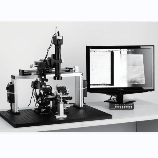
#Optical Waveguide Alignment System
Explore tagged Tumblr posts
Visit Tumblr Blog
Explore Tumblr blogs with no restrictions, modern design and the best experience.
Last Seen Tumblr Blogs


Fun Fact
Tumblr.com is the 103rd most visited website in the world.
Text
Chip-Scale Photonic Packaging: A New Era for Optical Fiber and Waveguide Alignment Systems
The emergence of chip-scale photonic packaging is a significant shift in optics. Manufacturers are concentrating on developing ultra-precise alignment systems to accommodate this miniaturization as the market for quicker, smaller, and more energy-efficient optical equipment expands. Here, the Optical Waveguide Alignment System and the Optical Fiber Alignment System are both being…
View On WordPress
0 notes
Text
Photonic IC Market Growth Signals Shift to Optical Data Technologies

The global Photonic Integrated Circuits (PIC) market was valued at US$ 10.2 Bn in 2022 and is projected to reach US$ 98.7 Bn by 2031, expanding at an impressive CAGR of 29.2% from 2023 to 2031. This growth is driven by rapid technological advancements, increasing demand for high-speed communication networks, and the adoption of photonics in space and computing technologies.
Market Overview
Photonic Integrated Circuits (PICs) are revolutionizing how data is transmitted and processed. Unlike traditional electronic ICs that utilize electrons, PICs employ photons (light) for data transmission, enabling high-speed, low-power, and high-bandwidth performance. These circuits integrate lasers, modulators, detectors, and waveguides into a compact substrate, significantly improving efficiency and miniaturization.
Analysts highlight the surging demand for high-speed networks, the increasing integration of photonics in aerospace and defense, and the emergence of AI, quantum computing, and cloud data centers as key factors accelerating the PIC market.
Market Drivers & Trends
High-Speed Communication Needs: With a global explosion in data traffic—driven by video streaming, cloud computing, and 5G—the need for faster, more energy-efficient data transmission solutions is paramount. PICs, with their superior bandwidth capabilities, are meeting this demand.
Space Exploration Boom: Space missions require components that can withstand extreme environments. PICs provide radiation tolerance, high precision, and secure communications, making them ideal for satellite communication, Earth observation, and deep space missions.
Rise of Hybrid Integration: Hybrid integration—accounting for over 53% of the market in 2022—allows manufacturers to combine multiple materials and components to build highly efficient and multifunctional PICs.
Silicon Photonics Dominance: Silicon is emerging as the most preferred raw material due to its cost-effectiveness, scalability, and alignment with existing semiconductor manufacturing processes.
Latest Market Trends
Adoption of Silicon Photonics in Data Centers: Growing energy consumption in data centers has led to the integration of silicon-based PICs for high-speed optical interconnects.
Miniaturization & System-on-Chip Advances: Manufacturers are heavily investing in miniaturized PICs that enable dense integration and compact design, particularly in medical and quantum devices.
Edge Computing & AI: The growing deployment of AI workloads and edge devices is creating new demand for fast, low-latency optical communication, fueling PIC adoption.
Key Players and Industry Leaders
The global PIC industry features numerous prominent companies, including:
Broadcom Inc.
Cisco Systems, Inc.
Intel Corporation
Infinera Corporation
Ciena Corporation
Lumentum Holdings, Inc.
Huawei Technologies Co., Ltd.
Coherent Corp.
Lightwave Logic, Inc.
MACOM
Nokia Technologies
These players are continuously launching next-generation PICs, forming strategic alliances, and acquiring niche startups to strengthen their portfolios.
Access important conclusions and data points from our Report in this sample - https://www.transparencymarketresearch.com/sample/sample.php?flag=S&rep_id=997
Recent Developments
Intel Labs (Dec 2022): Successfully demonstrated seamless integration of photonics with CMOS, paving the way for large-scale deployment of optical interconnects in computing chips.
Cisco (May 2022): Integrated advanced predictive analytics into its visibility and observability solutions to optimize PIC-based communication infrastructure.
Market Opportunities
Quantum Computing & Biophotonics: PICs are vital in enabling quantum optics, optical metrology, and biophotonics, including lab-on-a-chip diagnostics and biosensors.
Emerging Markets in Asia Pacific: Explosive growth in computing device production, especially in China, Japan, and India, is opening up large-scale manufacturing and application opportunities.
Sustainable Infrastructure: Energy-efficient PICs support the green transition in telecom and cloud services by reducing power consumption across data transmission systems.
Future Outlook
The future of the Photonic Integrated Circuits market looks robust, with continuous innovations in hybrid integration, advanced packaging, and material science. The emergence of 6G, AI-driven networks, quantum communications, and ultra-fast computing will further intensify the demand for photonic solutions.
PICs are expected to become foundational to next-gen digital infrastructure, providing the backbone for high-speed, secure, and energy-efficient information processing.
Market Segmentation
By Integration Type:
Monolithic Integration
Hybrid Integration (Dominant Segment)
Module Integration
By Raw Material:
Indium Phosphide
Gallium Arsenide
Lithium Niobate
Silicon (Fastest Growing, CAGR 34.1%)
Silicon-on-Insulator
Others
By Component:
Lasers
Waveguides
Modulators
Detectors
Optical Amplifiers
Multiplexers/De-multiplexers
Attenuators
By Application:
Optical Communication
Microwave/RF Photonics
Optical Signal Processing
Quantum Optics
Biophotonics
Medical Instrumentation
Transport & Aerospace
Energy & Utilities
Regional Insights
North America: Holds the largest market share due to its massive data center footprint, particularly in the U.S. (around 2,700 data centers). High investment in advanced telecom infrastructure and defense R&D fuels further growth.
Asia Pacific: Experiencing rapid expansion, led by China, which is the world’s largest exporter of computing devices. Rising government initiatives in semiconductors and digital transformation are propelling the market.
Europe: A strong contributor to quantum optics and medical photonics. Countries like Germany and the Netherlands are actively investing in integrated photonics R&D.
Frequently Asked Questions (FAQs)
Q1. What is the projected market size of the PIC industry by 2031? A1. The Photonic Integrated Circuits market is expected to reach US$ 98.7 Bn by 2031.
Q2. What is the CAGR for the market during the forecast period? A2. The market is set to grow at a CAGR of 29.2% from 2023 to 2031.
Q3. Which region holds the dominant share in the market? A3. North America, led by the U.S., dominates the global market.
Q4. What are the key factors driving market growth? A4. Increasing demand for high-speed communication, space exploration technologies, and hybrid integration advancements.
Q5. Which raw material is expected to see the fastest growth? A5. Silicon, due to its scalability, cost-effectiveness, and established manufacturing ecosystem.
Q6. Who are the major players in the PIC market? A6. Notable players include Intel, Cisco, Broadcom, Ciena, Lumentum, and Huawei.
Explore Latest Research Reports by Transparency Market Research:
Non-destructive Testing Market: https://www.transparencymarketresearch.com/non-destructive-testing-market.html
Microgrid Controller Market: https://www.transparencymarketresearch.com/microgrid-controller-market.html
Micro-electromechanical System (MEMS) Market: https://www.transparencymarketresearch.com/micro-electromechanical-system-market.html
IR Spectroscopy Market: https://www.transparencymarketresearch.com/ir-spectroscopy-market.html
Electronic Toll Collection System Market: https://www.transparencymarketresearch.com/electronic-toll-collection-system-market.html
About Transparency Market Research Transparency Market Research, a global market research company registered at Wilmington, Delaware, United States, provides custom research and consulting services. Our exclusive blend of quantitative forecasting and trends analysis provides forward-looking insights for thousands of decision makers. Our experienced team of Analysts, Researchers, and Consultants use proprietary data sources and various tools & techniques to gather and analyses information. Our data repository is continuously updated and revised by a team of research experts, so that it always reflects the latest trends and information. With a broad research and analysis capability, Transparency Market Research employs rigorous primary and secondary research techniques in developing distinctive data sets and research material for business reports. Contact: Transparency Market Research Inc. CORPORATE HEADQUARTER DOWNTOWN, 1000 N. West Street, Suite 1200, Wilmington, Delaware 19801 USA Tel: +1-518-618-1030 USA - Canada Toll Free: 866-552-3453 Website: https://www.transparencymarketresearch.com Email: [email protected]
0 notes
Text
The Silent Enabler: How IC Substrates Power the Semiconductor Revolution
Breaking Down the IC Substrate Ecosystem
The global IC substrate market has transformed into a $14.6 billion industry (Yole Développement 2025), driven by three core technology segments:

Advanced Packaging Platforms
2.5D/3D IC substrates now enable 12-layer interposers with <1μm alignment precision
Fan-out wafer-level packaging (FOWLP) achieves 0.8μm line/space resolution
Heterogeneous integration substrates support 10+ chiplet configurations
Material Science Breakthroughs
Low-loss dielectrics (Dk<3.0 @ 100GHz) from 8 major chemical suppliers
Nanocomposite thermal interface materials with 15W/mK conductivity
Photosensitive dielectric films enabling 2μm laser patterning
Cutting-Edge Manufacturing Innovations
Leading manufacturers have deployed:
AI-Optimized Production
Neural networks reducing warpage by 40% through real-time parameter adjustment
Digital twin systems predicting yield with 98.7% accuracy
Automated optical inspection achieving 50 defects per billion opportunities
Sustainable Manufacturing
Closed-loop chemical recycling recovering 92% of process materials
Plasma treatment replacing chemical desmear in 35% of facilities
Waterless cleaning systems reducing H2O usage by 8,000 tons/month per fab
Transformative Applications
AI/ML Hardware
NVIDIA's Blackwell GPU platform uses IC substrates with:
8μm microbump pitch
16-layer build-up structure
3D through-silicon via (TSV) integration
Automotive Electronics
Tesla's Dojo 2 training system incorporates:
45μm coreless substrates
Embedded decoupling capacitors
10μm ultra-fine line circuitry
Emerging Technology Frontiers
Quantum Computing
Cryogenic substrates operating at 4K with:
Superconducting niobium interconnects
Quantum-limited loss dielectrics
Magnetic field shielding layers
Biomedical Interfaces
Neural implant substrates featuring:
500nm flexible polyimide circuits
Biocompatible gold metallization
10-year in-vivo stability
Frequently Asked Questions
Why are IC substrates crucial for chiplet designs?
They provide:
Known-good-die (KGD) testing infrastructure
Ultra-short inter-chiplet links (<100μm)
Thermal stress buffering between heterogeneous dies
How do IC substrates enable 6G communications?
Through:
Terahertz waveguides with 0.001dB/mm loss
Antenna-in-package integration
3D electromagnetic shielding structures
What's the roadmap for IC substrate technology?
Key milestones include:
2026: 1μm line/space volume production
2028: Photonic interposer commercialization
2030: Molecular-scale self-assembling substrates
1 note
·
View note
Text
Xanadu Achieves Scalable Gottesman–Kitaev–Preskill States

States Gottesman–Kitaev–Preskill
Xanadu leads photonic quantum computing with their development of a scalable building block for fault-tolerant quantum computers. The achievement involves on-chip Gottesman–Kitaev–Preskill state production and was initially reported in January 2025 by Nature and summarised in June 2025. “First-of-its-kind achievement” and “key step towards scalable fault-tolerant quantum computing” describe this work.
Understanding GKP States' Importance
GKP states are error-tolerant photonic qubits. These complex quantum states consist of photons stacked in specific ways. Due to its unique structure, quantum error correcting methods may identify and fix phase shifts and photon loss. Zachary Vernon, CTO of Xanadu, calls GKP states “the optimal photonic qubit” because they enable quantum logic operations and error correction “at room temperature and using relatively straightforward, deterministic operations.” It has always been challenging to construct high-quality Gottesman–Kitaev–Preskill States on an integrated platform. This discovery advances continuous-variable quantum computing architectures by overcoming that obstacle.
GKP states provide fault-tolerant computing by using linear optics and measurement algorithms, unlike probabilistic entanglement methods that require repeated trials and complex feed-forward control. They fit well with hybrid systems because they generate quantum networks that link chips or modules or create larger cluster states for measurement-based computation.
Quantum systems' interoperability with optical fibre makes scaling easy, allowing them to be distributed among system components or data centres. This demonstration changed photonic quantum computing by taking a different approach from superconducting and trapped-ion platforms and bringing these systems closer to utility-scale quantum machine error thresholds.
Aurora: Photonic Quantum Computing Architectur
The “sub-performant scale model of a quantum computer” “Aurora” represents Xanadu's work. This system uses scalable, rack-deployed modules connected by fibre optics to incorporate all basic components. With 35 photonic devices, 84 squeezers, and 36 photon-number-resolving (PNR) detectors, Aurora provides 12 physical qubit modes each clock cycle. All system components except the cryogenic PNR detection array are operated by a single server computer and fit into four server racks.
Aurora's key technologies and their functions:
Silicon nitride waveguides feature minimal optical losses. This waveguide uses 300 mm wafers, which are common in semiconductor production. Newer chips based on Ligentec SA's 200-mm silicon-nitride waveguide architecture show potential for better squeezing and lower chip-fiber coupling losses.
The efficiency of photon-number-resolving (PNR) detectors is above 99%. In 12-mK dilution coolers, 36 transition edge sensor (TES) arrays form its base. These TES detectors cycle at 1 MHz and detect up to seven photon counts with little miscategorization error. Despite being highly effective, PNR detection efficiencies of over 99% are needed to meet the architecture's strict P1 path loss constraints.
Loss-optimized optical packaging—including accurate alignment, chip mounting, and fibre connections—was emphasised. This protects critical quantum information during routing and measurement.
The refinery array has six photonic integrated circuits (PICs) on a thin-film lithium-niobate substrate. Each refinery's two binary trees of electro-optic Mach-Zehnder modulator switches dynamically select the best output state based on PNR detection system feedforward instructions. Even though current Aurora refinery chips use probability-boosting multiplexing and Bell pair synthesis, future generations will use homodyne detectors to complete the adaptive breeding method.
Interconnects: Phase- and polarization-stabilized fiber-optical delay lines connect the refinery to QPU and refinery modules. These delays allow temporal entanglement and buffer information heralding in the cluster state.
Experiments and Results
Two large trials benchmarked Aurora's main features.
To generate a 12 × N-mode Gaussian cluster state, the system was set to send squeezed states to the QPU array. Data was collected at 1 MHz for two hours to synthesise and measure a macronode cluster state with 86.4 billion modes. Despite substantial optical losses (approximately 14 dB), the nullifier variances remained below the vacuum noise threshold, proving squeezing and cluster state entanglement.
Detecting Repetition Code Errors: This experiment showed the system's feedforward and non-Gaussian-state synthesis using low-quality GKP states. In real time, the QPU decoder assessed the system's two (foliated) repetition code checks. The decoder calculated bit values and phase error probabilities to change the measurement basis for the next time step.
Limitations and Prospects
Despite these notable examples, the “component performance gap” between existing capabilities and fault tolerance needs remains large. The main limiter of quantum state purity and coherence is optical loss. Ideal designs for fault-tolerant operation require loss budgets of about 1%, whereas the Aurora system lost 56% for heralding pathways (P1) and nearly 95% for heralded optical paths (P1 and P2).
Xanadu's future projects include:
Hardware improvements: Chip fabrication, waveguide geometry, and packaging are optimised to improve fidelity and reduce optical loss. The photonic components' insertion loss must be improved by 20-30 times (on a decibel scale).
Architectural Refinements: Testing cutting-edge hardware-level photon generation and detection rates and error mitigation measures to reduce loss and imperfection.
Integration and Scaling: combining the new GKP generation methods with Aurora's networking, error correcting protocols, and logic gates. The company believes scalable, semiconductor-compatible platforms can mass-produce, modify, and monitor error-correcting components for modular quantum computing.
Even though quantum hardware across all platforms is currently in the noisy intermediate-scale quantum (NISQ) period, Xanadu's work shows how to scale photonic quantum computers to address real applications. Fiber-optical networking, classical control electronics, and photonic-chip fabrication can scale and modularise a realistic photonic architecture. We must continuously improve optical GKP-based architectures to find the most hardware-efficient and imperfection-tolerant systems.
#GottesmanKitaevPreskillState#GKPstates#physicalqubit#QuantumProcessingUnit#Xanadu#quantumcomputing#News#Technews#Technology#Technologynews#Technologytrends#Govindhtech
0 notes
Text
Have your PIC-based devices been tested reliably and quickly?
Photonic Integrated Circuit (PIC) solutions are being adopted by manufacturers to address the reduced size and complexity challenges while also addressing heat management issues experienced in today’s data centres. Frantic development of smaller, faster, cheaper and greener transceivers/active components and passive components is driving the development of high-speed networks and 5G, Photonic Integrated Circuits (PICs).
Passive optical components used in optical systems operate without external power or active control. They use processes such as transmission, reflection, polarisation, coupling, splitting, filtering, and attenuation to alter light signals.
Need for Testing
A PIC is composed of many optical components such as optical couplers, fibre-optic switches, splitters, attenuators, wavelength-division multiplexers, and transceivers.
Testing of any PIC-based device is needed in all life cycle stages — from design and development, and qualification to validation of production.
Testing – The Requirements
Automation, repeatability, scalability and parallelisation of the testing processes are needed for the huge volume of circuits and ports, to be able to meet the profitability of economies of scale. Photonics labs must evolve with the optical test requirements of passive (guiding light) optical components.
The fast maturing PIC die manufacturing has given rise to photonic wafers containing thousands of components made available by foundries through Process Design Kits (PDKs). Reliable testing is needed to optimise the different parameters of a given optical component.
Testing – The Challenges
Accuracy/repeatability: Obtaining traceable results for tight acceptance thresholds and greater yield of known good dies.
Dynamic range: Seeing full optical spectral contrast in a single measurement.
Speed: Keeping alignment and measurement time to a minimum, but also accelerating the ease of the test and analysis iterative flow.
From data to insight: Generating and managing structured data that is ready for artificial intelligence and business intelligence.
Flexible/scalable: Leveraging test station modularity and third-party compatibility of software to improve test throughput and complexity over time or swap equipment as needed.
Automation: Automating chip and wafer advanced navigation to control any instrument and execute data analysis in user-defined test routines to test massive circuits with minimal cost of ownership.
Testing PIC-based passive components is challenging due to the high port count of some components like Arrayed Waveguide Grating (AWG) and the huge number of components to test on a single die. A component test platform operates in conjunction with a continuously tunable laser to measure optical insertion loss, return loss and polarisation-dependent loss across the laser’s spectral range. Optical spectrum must be realised quickly and with a high wavelength resolution, typically to the order of a picometer.
Testing – The Process
The PIC devices are usually tested at the wafer level prior to dicing to detect defects as early as possible and to avoid packaging defective dies.
Using a PIC wafer probe station, light is coupled into the wafer to enable measurement of the optical characteristics of the DUT.
Testing Solutions for Photonics from MELSS
MELSS brings you Test and Measurement (T&M) hardware and software solutions from market leaders EXFO, which are automated, scalable, fast, accurate and cost-optimised. These T&M solutions range from those for Passive and Active components as well as automated probe stations for wafer and single-die testing.
The OPAL series of probe stations deliver industry-leading performance for testing wafers, multiple as well as single dies, enabling accurate, repeatable and fast measurement. The PILOT software suite offers automation capabilities that support the full test flow (preparation through measurement to results analysis), using EXFO’s or third-party T&M instruments.
EXFO’s comprehensive range of optical testing solutions includes component test platforms, optical testing solutions, light sources, benchtop tunable lasers, passive component testers, optical spectrum analysers, tunable filters with adjustable bandwidth, variable attenuators, switches and power meters.
EXFO has developed automated, scalable, fast, accurate and cost-effective Test and Measurement (T&M) hardware and software solutions. Ranging from simple optical testing to spectral optical characterisation or traffic analysis, EXFO offers an extensive selection of probe stations for wafer, bar, multi-die or single die configurations, and a powerful automation software suite.
The CTP10 from EXFO specifically addresses key PIC measurement challenges. measuring optical components quickly, reliably and accurately.
The CTP10 is a modular component test platform that operates together with the T200S or T500S continuously tunable lasers. The CTP10 characterises the spectral properties of high port count devices in one single scan with
High spectral resolution
70-dB dynamic range, even at a sweep speed of 200 nm/s
Operation from 1240 to 1680 nm
Coverage of a wide range of applications, including telecom, sensing and LIDAR.
Both optical and photocurrent measurements with analog output for PIC first-light search and coupling optimisation
Fast data transfer
Remote control using SCPI commands is possible
Increased PIC testing throughput
Reduced test time
High sampling resolution of 20 fm
Accurate measurement of narrow spectral features
The CT440 is a compact variant of the CTP10, with the same performance – ideal for the characterisation of PIC components with limited outputs.
In addition to the above range of products, EXFO produces other advanced products such as the T200S, T500S, CTP10, CT440, OSICS T100, FTBx-2850 and OSA20.
Author: MELSS
0 notes
Video
youtube
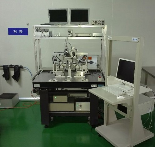
Fibermart provides Fiber Waveguide Alignment Stages for Fiber Array to Chip, Chip to Chip coupling alignment. With software controlled automated alignment, dispention and UV curing. See more infos at https://www.fiber-mart.com/optical-fiber-waveguide-alignment-system-c-73_515_848.html Contact [email protected] for sale. Thank you!
1 note
·
View note
Text
The Revolutionary Application of Quartz Plate in Semiconductor Packaging
The Revolutionary Application of Quartz Plate in Semiconductor Packaging: Why These Four Designs Are Game-Changers Let’s cut through the noise: semiconductor packaging isn’t just about chips anymore—it’s about the materials that cradle them. Quartz plates, once relegated to lab equipment, are now the unsung heroes of microelectronics. But not all quartz is created equal.
I’ve seen firsthand how four specific designs—round transparent quartz glass plates, tempered quartz sight glass, OEM customized optical square/round quartz glass plates, and square UV transparent quartz plates—are rewriting the rules of reliability and precision. Here’s why they matter.
1. Round Transparent Quartz Glass Plates: The Purity Powerhouse
Imagine a material so pristine it makes surgical steel look rusty. Round transparent quartz plates, with >99.99% SiO₂ purity, are the gold standard for wafer handling in extreme environments. Take TSMC’s 3nm node fab: by replacing ceramic carriers with these plates, they reduced particulate contamination by 78% during high-temperature annealing1. The secret? Zero metallic ions means no unwanted doping—critical when a single stray atom can wreck a billion-transistor chip.
But purity isn’t their only trick. Their thermal stability (up to 1,200°C) allows rapid thermal processing (RTP) cycles without warping—a feat that aluminum nitride plates fail at after 50 cycles.
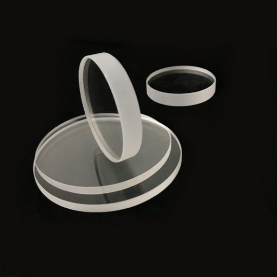
2. Tempered Quartz Sight Glass: When Failure Isn’t an Option
Vacuum chambers in EUV lithography systems demand visibility and invincibility. Tempered quartz sight glass, chemically strengthened via ion exchange, laughs at 10⁻⁸ Torr pressures while providing distortion-free inspection windows. ASML’s latest EUV machines use these panels to monitor plasma arcs—where standard fused silica would cloud within weeks under 13.5nm radiation.
The kicker? Their surface hardness (9 Mohs) prevents scratches from robotic handlers—eliminating the “fogged window” failures that once caused 12% of lithography tool downtime.
3. OEM Customized Optical Square/Round Quartz Plates: Geometry Meets Photonics
Why settle for off-the-shelf when light manipulation demands perfection? Customized optical quartz plates, with sub-λ/4 flatness, are enabling breakthroughs in chip-scale photonics. Intel’s optical interconnects team credits square quartz plates—etched with nanoscale grating patterns—for achieving 92% light coupling efficiency in their silicon photonics modules12. The rectangular edges align perfectly with waveguide arrays, something round plates can’t match.
But round variants shine too: their radial symmetry minimizes stress birefringence in laser diode packaging—a must for 800G DR4 transceivers.
4. Square UV Transparent Quartz Plates: The Dark Horse of Advanced Packaging
UV-curing adhesives are the glue holding 2.5D/3D packages together—literally. Square UV quartz plates, transmitting >90% at 254nm, ensure uniform curing while blocking IR heat that warps interposers. Samsung’s HBM4 stack line reported a 30% yield boost after switching to these plates, as their sharp corners align with die edges to prevent adhesive bleed-out.
Bonus: Their UV transparency doubles as a built-in quality check—uncured resin fluoresces under 365nm light, visible through the plate.

Why This Isn’t Just Progress—It’s a Paradigm Shift
Critics argue quartz is “too brittle” or “too niche.” Tell that to the engineers who’ve seen:
Round plates slash cleanroom particle counts by filtering airborne contaminants during robotic transfers.
Square UV plates enable fan-out wafer-level packaging (FOWLP) for wearables, where 0.1mm thickness tolerances are non-negotiable.
While graphene and GaN hog headlines, quartz plates work silently in the trenches—enabling the angstrom-scale precision our connected world demands.
The Bottom Line In semiconductor packaging, the difference between “functional” and “flawless” lies in the materials you trust. These four quartz plate designs aren’t just components—they’re enablers of a future where chips aren’t just smaller, but smarter. If your supply chain hasn’t embraced them yet, you’re not just behind the curve—you’re ignoring the bedrock of modern electronics.
0 notes
Text
Environmental considerations for Optical Waveguide Alignment
Environmental considerations for optical waveguide alignment are crucial in ensuring the reliability, performance, and sustainability of optical communication systems. Here are some key environmental factors to take into account: 1. Temperature and Humidity Control:Optical waveguides are sensitive to changes in temperature and humidity. Variations in these environmental conditions can cause…
0 notes
Text
[ad_1] Lighting, additionally often known as luminaires, are available in quite a lot of sizes, shapes, and wattages. The diagram under reveals the principle kinds of devices. Clearly, there are various completely different varieties of every kind of fixture. There are additionally articles discussing varied elements of lighting. So what's a Gentle Fixture? A mild fixture is a lighting meeting that features a number of mild sources and parts designed to distribute the sunshine, place and shield the lamps, and join the lamps to an influence provide. The primary operate of a luminaire is to aesthetically modify the form of the sunshine supply and management the distribution of the emitted mild. A lighting fixture's electrical system offers energy, management, or different electrically-based features, corresponding to wires, sockets, switches, drivers, connectors, circuits, and sensors. Optical parts might embrace diffusers, lenses, prismatic components, waveguides, reflectors, refractors, louvers, and so on. LED lights promise excessive luminous output, power effectivity and lengthy lifespan, making them appropriate for a lot of lighting purposes that had been beforehand the area of lighting. Incandescent or fluorescent lights. The sunshine supply of an LED lighting fixture will be an LED bulb or an built-in LED module. What's the distinction between lighting and becoming lights? Fixtures are objects which can be usually hooked up or mounted to the property, whereas fittings are objects that aren't hooked up to the property aside from nails or screws, corresponding to work or mirrors. How do I select a great mild fixture? When selecting a mild fixture, begin along with your favourite components within the room and discover lighting that enhances them. For instance, you probably have a fashionable couch, clean-lined lighting will make the house stand out. One other tip is to take a look at the cabinetry or door hardware within the room and select fixtures with complementary finishes. What does lighting embrace? Lighting may additionally produce other options, corresponding to a reflector to direct the sunshine, an aperture with or and not using a lens, an outer shell or housing to align and shield the lamps, an electrical ballast or energy provide, and a shade to diffuse the sunshine. Activate a light-weight or level it in the direction of your work space. What do lighting fixtures do? Lighting present mild. They can be utilized as ornamental components in a house or constructing, or they can be utilized for sensible functions, corresponding to offering lighting in areas which can be usually unlit. Lighting may improve security by illuminating darkish areas of a constructing the place individuals might journey on one thing and injure themselves. How do lighting fixtures work? Lighting work by changing electrical energy into mild. They do that utilizing mild bulbs, that are units that comprise an electrical present and produce mild when switched on. The sunshine bulb itself is a part of the fixture that's seen whenever you activate the lights in your house or workplace. The second piece of kit on most lighting fixtures is named an electrical socket (or field), which incorporates all of the wall-mounted electrical retailers you may plug issues into. The place are lighting used? You've got most likely seen it at residence. However the place do the sunshine fixtures really go? There are various locations in your house the place you need to use lighting. For instance, within the kitchen, rest room and bed room, that you must take into account what sort of ambiance you wish to create with every fixture. for instance: 1. Bed room: Use an under-bed lamp with a job lighting function, corresponding to a dimmer swap, to keep away from disturbing others making an attempt to sleep. 2. Kitchen: If it is a brilliant, sunny day exterior and you do not want overhead lighting as a result
of it is obscured by window frames or cupboards, and you are not cooking at evening, ambient lighting will most likely suffice! 3. Lavatory: Darkish interiors might imply the reply is to make use of overhead lighting with a number of bulbs so they do not come on on the similar time when somebody opens the lavatory door. Regularly Requested Questions Are ceiling lights fixtures? Ceiling kind of fixture mounts on to the ceiling and has a glass or plastic shade that obscures the bulb. Ceiling fixtures have been widespread in houses for practically 100 years, typically offering all of the ambient lighting for a room. What's the best peak for kitchen pendant lights? The best peak of your kitchen pendant lights will depend upon quite a lot of components, together with ceiling peak and lighting goal. As a normal guideline, pendant lights ought to be hung about 32 to 36 inches above your kitchen island or countertop. Nevertheless, modify the peak in accordance with your private desire and the particular wants of your kitchen. What's the goal of a lighting fixture? Lighting present mild. They can be utilized as ornamental components in a house or constructing, or they can be utilized for sensible functions, corresponding to offering lighting in areas which can be usually unlit. Can I set up recessed lighting in a kitchen with a low ceiling? Sure, recessed lighting will be put in in kitchens with low ceilings. Nevertheless, it is very important take into account the obtainable house and depth of recessed lighting. To make sure correct set up and keep away from potential clearance points, select shallow or slim recessed lighting designed particularly for low ceilings. [ad_2] Supply hyperlink
0 notes
Text
arkoptics.com
A passive multiplexer in most networks consists of a mux and demux optical component. The mux combines, or multiplexes, wavelengths onto a fiber. The demux on the other end of the connection splits, or de-multiplexes, the connections.
In DWDM system, DWDM mux demux is two indispensable modules. Mux (Multiplexer) is a module at the transmitter end that brings several data signals together for transporting over a single fiber, while Demux (Demultiplexer) is a module at the receiver end that separates the signals that come together and passes each channel to an optical receiver.
CWDM mux demux (Coarse Wavelength Division Multiplexer/Demultiplexer) is a flexible, low-cost solution that enables the expansion of existing fiber capacity. CWDM multiplexer is for combining signals together, while demultiplexer is for splitting signals apart.
A polarization-maintaining (PM) WDM filter is a small device used to multiplex PM signals while maintaining the output polarization. When you are using highly efficient systems, PM fibers and PM signals play a very critical role in ensuring the desired efficiency.
Fiber Patch Cord & Cable Assembly, often called fiber patch cable, fiber jumper, or fiber patch lead, is a length of fiber cable that terminated with fiber optic connectors (LC, SC, MTRJ, ST and etc.) at each end. The connectors allow fiber optic patch cord to be rapidly connected to an optical switch or other telecommunications/computer device.
Fiber loopback is widely used for various applications. In terms of telecommunication, loopback is a hardware or software method to feed a received signal or data back to the sender. It is very useful for solving physical connection problems.
Fiber terminators(Plug-in type or Build-out type) are used to terminate unused fiber connector ports in fiber optic systems so optical terminators unwanted reflections are not introduced back into the system. It is used in the fiber-optic networks to install on possibly unused ports.
Fiber optic isolator is a passive component used for fiber optic communications. As a magneto-optic device, the purpose of optical isolator is to allow light to be transmitted in only one direction. An optical isolator is a device that is designed to allow the optical signal travel in the forward direction while block reflections that would travel in the backward direction. Optical isolators are critically important in many applications in optical systems.
FBT splitter(fused biconical taper) is the traditional technology in which two fibers are placed closely together, typically twisted around each other and fused together by applying heat while the assembly is being elongated and tapered. A signal source controls the desired coupling ratio. The fused fibers are protected by a glass substrate and then protected by a stainless steel tube, typically 3 mm diameter by 54 mm long. FBT splitters are widely accepted and used in passive optical networks.
The PLC splitters are used to separate or combine optical signals. A PLC (planar lightwave circuit) is a micro-optical component based on planar lightwave circuit technology and provides a low-cost light distribution solution with small form factor and high reliability. PLCs are manufactured using silica glass waveguide circuits that are aligned with a v-groove fiber array chip that uses ribbon fiber. Once everything is aligned and bonded, it is then packaged inside a miniature housing. PLC splitters have high quality performance, such as low insertion loss, low PDL, high return loss, etc.
1 note
·
View note
Text
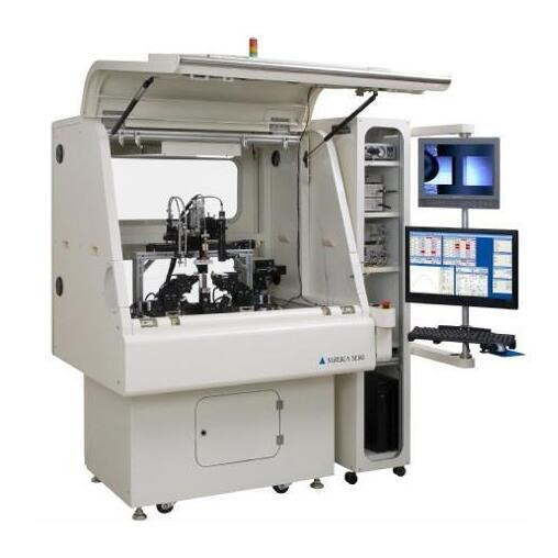
Optical Fiber Alignment Systems Are Revolutionizing Next-Gen Communication Networks
Precision is crucial in the ever changing field of communication technology. The need for quicker, more dependable connections is only increasing, whether it is via 5G networks, high-speed internet, or data centres that fuel the cloud. The Optical Fiber Alignment System is a quiet but significant invention that is working behind the scenes.
An optical fibre alignment system: what is it?
A high-precision method for aligning optical fibres with nanometre accuracy is called an optical fibre alignment system. By ensuring that the cores of two fibres are precisely aligned, these systems reduce insertion loss and increase signal strength. Even the most sophisticated fibre networks will experience inefficient transmission in the absence of precise alignment.
Why is Alignment Important?
Networks are under more strain than ever before due to the exponential increase in data consumption—think video streaming, remote work, IoT, and AI. Accurately aligning optical components has a direct impact on:
Transmission Speed: Data transport may be slowed down by misalignment.
Signal Quality: Signal loss is decreased by precise alignment.
Network Reliability: Outages and error rates are increased by faulty connections.
Optical Waveguide Alignment System
The Optical Waveguide Alignment System goes beyond conventional alignment, which just considers fibres. It is intended to align integrated photonic waveguides as well as optical fibres, which are crucial parts of photonic chips that manage light-based data transfer on a micro scale.
These systems are necessary in:
Faster, smaller, and more energy-efficient circuits are made possible via silicon photonics.
In quantum computing, accuracy cannot be compromised.
Advanced Sensing: When photonic integration is needed in aeronautical or healthcare applications.
Optical Waveguide Alignment Systems are driving innovation in a variety of sectors by guaranteeing nearly flawless coupling between fibres and waveguides. The foundation of tomorrow's communication infrastructure is made up of Optical Fiber Alignment System and optical waveguide alignment systems, which may enhance the quality of your video conversations and enable cutting-edge technologies like photonic chips and quantum computing.
Next: PM Fiber Patch Cables: What They Are and Why They Matter
1 note
·
View note
Text
Science and Chemistry Classes
New polymer materials make fabricating optical interconnects easier
Researchers have developed new polymer materials that are ideal for making the optical links necessary to connect chip-based photonic components with board-level circuits or optical fibers. The polymers can be used to easily create interconnects between photonic chips and optical printed circuit boards, the light-based equivalent of electronic printed circuit boards.
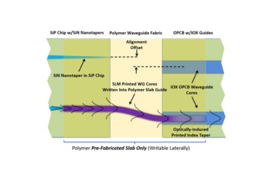
"These new materials and the processes they enable could lead to powerful new photonic modules based on silicon photonics," said research team leader Robert Norwood from the University of Arizona. "They could also be useful for optical sensing or making holographic displays for augmented and virtual reality applications.
Silicon photonics technology allows light-based components to be integrated onto a tiny chip. Although many of the basic building blocks of silicon photonic devices have been demonstrated, better methods are needed to fabricate the optical connections that link these components together to make more complex systems.
In the journal Optical Materials Express, the researchers report new polymer materials that feature a refractive index that can be adjusted with ultraviolet (UV) light and low optical losses. These materials allow a single-mode optical interconnect to be printed directly into a dry film material using a low cost, high throughput lithography system that is compatible with the CMOS manufacturing techniques used to make chip-based photonic components.
"This technology makes it more practical to fabricate optical interconnects, which can be used to make the Internet—especially the data centers that make it run—more efficient," said Norwood. "Compared to their electronic counterparts, optical interconnects can increase data throughput while also generating less heat. This reduces power consumption and cooling requirements."
Replacing wires with light
The research expands on a vinylthiophenol polymer material system known as S-BOC that the investigators developed previously. This material has a refractive index that can be modified using UV illumination. In the new work, the researchers partially fluorinated S-BOC to improve its light efficiency. The new material system, called FS-BOC, exhibits lower optical propagation losses than many other optical interconnect materials.
"With this material we can use a process that we call SmartPrint to directly write optical interconnections between different optical printed circuit board elements, such as ion-exchange (IOX) glass waveguides provided by our collaborator Lars Brusberg from Corning Incorporated," said Norwood.
To perform the SmartPrint process, a FS-BOC film is applied directly to a photonic component. No mechanical alignment is needed because the optical interconnect is made using a maskless lithography system that calculates where the interconnect is required by looking at the components and then writing the optical interconnect into the polymer using photoexposure. No additional processing is necessary other than briefly heating the polymer film to 90 °C. Because the fabrication approach is maskless, writing patterns can be changed without making a new photomask.
Creating a connection
To demonstrate the new materials, the researchers deposited them directly onto ion-exchange glass waveguide arrays, which are commonly used for integrated photonic devices. They then printed the coupling features needed to allow light to travel out of one IOX waveguide, propagate into the newly fabricated polymer interconnect, and then enter a second IOX waveguide adjacent to the initial IOX waveguide.
According to the researchers, the polymer optical interconnects worked well and showed low propagation and coupling losses, which means very little light was lost as it traveled within the interconnect or between it and the other components.
The researchers are now working to improve the material's refractive index contrast and performance at high temperatures. "A higher refractive index contrast would make the material more tolerant to manufacturing variations while high temperature performance is likely needed for the interconnect to withstand solder reflow processes, which take place above 200 °C," said Norwood.
0 notes
Text
Splitter
https://www.china-tscom.com/products/splitter/

PLC Splitter
As a professional plc splitter manufacturer, T & S Communication produces a planar optical waveguide chip on its own and manufactures PLC splitter with self-developed PLC aligning equipment for automatic coupling. T&S PLC splitter has a good consistency and stable quality. T&S has built 10000-class and 1000-class dust-free workshops, and there are 32 sets of automatic alignment systems. T&S plc splitter factory offers premium PLC splitters of various packaging types including bare fiber type, mini type, box type, cassette type, tray type and rack-mounted type PLC splitter are available. The current monthly production capacity is 200000 PCs (1x8).
FBT Coupler
T&S Communication coupler manufacturer provides a wide breadth of FBT couplers, which includes SM standard coupler, dual-window coupler, three-window coupler, wideband coupler with low insertion loss and high performances. The FBT couplers are available with a coupling ration ranging from 1:99 to 50:50. Customized specifications are basically available.
FBT Coupler is a type of splitter which is based on fused biconical taper technology. The technology is widely accepted and adopted in the PON solution. FBT or fused biconical taper is a traditional technology that two fibers are twisted and fused together under high temperature while the device is being elongated and tapered. As a professional coupler factory, T&S provides various kinds of high-quality FBT couplers.
0 notes
Text
Quantum Photonics: Improving Future Of Light-Based Computing

Quantum Photonics is analyzed on high-performance computers initially. A secret relationship between quantum photonics and classical high-performance computing may surprise you.
High-performance computing (HPC) software has been created by researchers at Paderborn University in Germany to study and characterize the quantum states of a photonic quantum detector.
Using sophisticated classical computers to handle massive datasets, carry out intricate computations, and quickly resolve difficult issues is known as high-performance computing, or HPC.
What Is Quantum Photonics?
The study of producing, modifying, and detecting light in regimes where individual quanta of the light field (photons) may be coherently controlled is known as quantum photonics.
What Is The Use Of Photonics?
Light is transformed into electrical impulses using photonic sensors. The energy sector uses this technology extensively. The most prevalent applications of photonic sensing are solar power and wind, oil, and geothermal energy monitoring.
In the past, it has been essential to investigating quantum phenomena, such as the Bell test experiments and the EPR conundrum. Future technologies including quantum metrology, quantum computing, and quantum key distribution are also anticipated to be greatly advanced by quantum photonics.
Because of their minimal decoherence characteristics, light-speed transmission, and simplicity of manipulation, photons are especially appealing as carriers of quantum information. Traditionally, “bulk optics” technology individual optical components (beamsplitters, lenses, etc.) installed on a massive optical table with a total mass of hundreds of kilograms was used in quantum photonics studies.
Integrated Quantum Photonics
One crucial step in creating practical quantum technology is the use of integrated quantum photonic circuits to quantum photonics. Compared to bulk optics, single die photonic circuits have the following benefits:
Miniaturization: A smaller system size results in an order of magnitude reduction in size, weight, and power consumption.
Stability: Waveguides and other components made from miniature parts using sophisticated lithographic processes are naturally phase stable (coherent) and don’t need optical alignment.
Experiment size: A device that is just a few square centimeters in size may have a large number of optical components.
Manufacturability: Devices may be produced in huge quantities at a much reduced price. Products based on this technology can be produced using current manufacturing processes and procedures since the elements used in Integrated Quantum Photonics are more easily miniaturized due to their well-developed fabrication techniques.
Parts: There are several practical distinctions between quantum and conventional photonic integrated circuits, despite the fact that both employ the same basic components. In quantum photonics, loss is the most important component as single photon quantum states cannot be amplified (no-cloning theorem).
Applications Of Quantum Photonics
Waveguides, directional couplers, and phase shifters are the building elements used to construct single photon sources. Increased nonlinear interaction for photon pair generation is typically provided by optical ring resonators and long waveguide sections, but efforts are also underway to integrate solid state systems single Waveguide photonic circuits for quantum dot and nitrogen-vacancy center photon sources.
Many applications for quantum photonics include:
Quantum communication: It may improve information security via QKD and other methods. Eavesdropping can be stopped using the non-cloning theorem.
Quantum computing: Quantum photonics may encode information in quantum bits (qubits) for faster processing.
Quantum photonic allows quantum simulation.
Using quantum photonics, quantum metrology may be accomplished.
Photonics might enable quantum teleportation.
Random number generators: Random numbers may be produced via quantum photonics.
Quantum Photonics Advantages
The advantages of quantum photonics are many and include:
Scalability
Large quantities of photonic integrated circuits (PICs) may be produced on a wafer, which saves money and time.
Compactness
Unlike optical benches, PICs incorporate optical components into a centimeter-long chip. High degrees of control over light and the generation, modification, and detection of light are made possible by control PICs.
Compatibility
Current silicon chip production techniques and telecom light sources are compatible with photonics.
Adaptability to the environment
Without the need of complex cooling techniques, photon-based computers can function at ambient temperature.
Effective storage
Compared to conventional hardware, photonic quantum computers have a more efficient amount of area for information storage.
Networks of quantum systems
Photonic quantum processors may be used as servers for distributed quantum computing resources or as repeaters for quantum error correction.
Component Of Quantum Photonic
Photons are used in quantum photonics to create and preserve quantum states for quantum processes. Compared to other possibilities, photons are a sensitive medium that is less impacted by electromagnetic interference. Because they may be utilized to create small, scalable, and highly effective devices, photonic integrated circuits (PICs) are an essential component of quantum photonic systems.
Read more on Govindhtech.com
#Highperformancecomputing#QuantumPhotonics#datasets#quantumcomputing#quantumphotonicsystems#News#Technews#Technology#technologynews#technologytrends#govindhtech
0 notes
Text
Have your PIC-based devices been tested reliably and quickly?
Photonic Integrated Circuit (PIC) solutions are being adopted by manufacturers to address the reduced size and complexity challenges while also addressing heat management issues experienced in today’s data centres. Frantic development of smaller, faster, cheaper and greener transceivers/active components and passive components is driving the development of high-speed networks and 5G, Photonic Integrated Circuits (PICs).
Passive optical components used in optical systems operate without external power or active control. They use processes such as transmission, reflection, polarisation, coupling, splitting, filtering, and attenuation to alter light signals.
Need for Testing
A PIC is composed of many optical components such as optical couplers, fibre-optic switches, splitters, attenuators, wavelength-division multiplexers, and transceivers.
Testing of any PIC-based device is needed in all life cycle stages — from design and development, and qualification to validation of production.
Testing — The Requirements
Automation, repeatability, scalability and parallelisation of the testing processes are needed for the huge volume of circuits and ports, to be able to meet the profitability of economies of scale. Photonics labs must evolve with the optical test requirements of passive (guiding light) optical components.
The fast-maturing PIC die manufacturing has given rise to photonic wafers containing thousands of components made available by foundries through Process Design Kits (PDKs). Reliable testing is needed to optimise the different parameters of a given optical component.
Testing — The Challenges
Accuracy/repeatability: Obtaining traceable results for tight acceptance thresholds and greater yield of known good dies.
Dynamic range: Seeing full optical spectral contrast in a single measurement.
Speed: Keeping alignment and measurement time to a minimum, but also accelerating the ease of the test and analysis iterative flow.
From data to insight: Generating and managing structured data that is ready for artificial intelligence and business intelligence.
Flexible/Scalable: Leveraging test station modularity and third-party compatibility of software to improve test throughput and complexity over time or swap equipment as needed.
Automation: Automating chip and wafer advanced navigation to control any instrument and execute data analysis in user-defined test routines to test massive circuits with minimal cost of ownership.
Testing PIC-based passive components is challenging due to the high port count of some components like Arrayed Waveguide Grating (AWG) and the huge number of components to test on a single die. A component test platform operates in conjunction with a continuously tunable laser to measure optical insertion loss, return loss and polarisation-dependent loss across the laser’s spectral range. The optical spectrum must be realised quickly and with a high wavelength resolution, typically to the order of a picometer.
Testing — The Process
The PIC devices are usually tested at the wafer level prior to dicing to detect defects as early as possible and to avoid packaging defective dies.
Using a PIC wafer probe station, light is coupled into the wafer to enable measurement of the optical characteristics of the DUT.
Testing Solutions for Photonics from MELSS
MELSS brings you Test and Measurement (T&M) hardware and software solutions from market leaders EXFO, which are automated, scalable, fast, accurate and cost-optimised. These T&M solutions range from those for Passive and Active components as well as automated probe stations for wafer and single-die testing.
The OPAL series of probe stations deliver industry-leading performance for testing wafers, multiple as well as single dies, enabling accurate, repeatable and fast measurement. The PILOT software suite offers automation capabilities that support the full test flow (preparation through measurement to results analysis), using EXFOs or third-party T&M instruments.
EXFOs comprehensive range of optical testing solutions includes component test platforms, optical testing solutions, light sources, benchtop tunable lasers, passive component testers, optical spectrum analysers, tunable filters with adjustable bandwidth, variable attenuators, switches and power meters.
EXFO has developed automated, scalable, fast, accurate and cost-effective Test and Measurement (T&M) hardware and software solutions. Ranging from simple optical testing to spectral optical characterisation or traffic analysis, EXFO offers an extensive selection of probe stations for wafer, bar, multi-die or single-die configurations, and a powerful automation software suite.
The CTP10 from EXFO specifically addresses key PIC measurement challenges. measuring optical components quickly, reliably and accurately.
The CTP10 is a modular component test platform that operates together with the T200S or T500S continuously tunable lasers. The CTP10 characterises the spectral properties of high port count devices in one single scan with
High spectral resolution
70-dB dynamic range, even at a sweep speed of 200 nm/s
Operation from 1240 to 1680 nm
Coverage of a wide range of applications, including telecom, sensing and LIDAR.
Both optical and photocurrent measurements with analog output for PIC first-light search and coupling optimisation
Fast data transfer
Remote control using SCPI commands is possible
Increased PIC testing throughput
Reduced test time
High sampling resolution of 20 fm
Accurate measurement of narrow spectral features
The CT440 is a compact variant of the CTP10, with the same performance — ideal for the characterisation of PIC components with limited outputs.
In addition to the above range of products, EXFO produces other advanced products such as the T200S, T500S, CTP10, CT440, OSICS T100, FTBx-2850 and OSA20.
Author MELSS
#collaborativerobots#industrialiotsolutionsindia#automatedtestequipmentmanufacturers#endofarmtooling#electricvehicletestsolutions#solderpaste#industrialautomationandrobotics
0 notes