#PCB material interpret
Explore tagged Tumblr posts
Visit Tumblr Blog
Explore Tumblr blogs with no restrictions, modern design and the best experience.
Last Seen Tumblr Blogs


Fun Fact
69% of Tumblr users are millennials.
Text
Tg, TD, CTI, Coefficient of thermal expansion (Tce), Dissipation factor, Electrical breakdown voltage DBV, Water absorption factor WA etc.all factors about PCB material to produce PCB,more details welcome to contact me
0 notes
Text
How to Prepare for a DMLT Career in Bhilwara
Introduction
Students interested in healthcare should consider the Diploma in Medical Laboratory Technology in Bhilwara as an outstanding career path. The diploma program provides students with necessary laboratory skills for diagnostic testing together with medical research abilities. The growing scope of healthcare covers a need for qualified medical laboratory technicians whose demand remains steadily increasing. To pursue a DMLT career in Bhilwara an effective preparation method and knowledge of educational development are essential and this document will guide you through this process accordingly.
Understanding the DMLT Course
A basic comprehension of the Diploma in Medical Laboratory Technology in Bhilwara needs to precede any preparation work.
Studying the Diploma in Medical Laboratory Technology takes a period of 1 to 2 years at most institutions.
Eligibility Criteria: A minimum qualification of 10+2 with Science (Physics, Chemistry, and Biology).
Clinical Biochemistry, Hematology, Microbiology and Pathology along with Lab Management make up the subjects of this course.
Career Opportunities: Medical labs, hospitals, diagnostic centers, research facilities, and pharmaceutical companies.
The following segments will outline your preparation strategy for obtaining success in DMLT career paths in Bhilwara.
1. Research and Choose the Right College
The process starts with choosing an established institution providing the Diploma in Medical Laboratory Technology in Bhilwara. Here’s what to consider:
Accreditation and recognition by medical councils or universities.
Experienced faculty and well-equipped laboratories.
Students can access internship opportunities in respected hospitals together with diagnostic labs.
Affordable fee structure and availability of scholarships.
The educational institutions providing DMLT training in Bhilwara include both public and private institutions among their top ranking programs. Check facilities available through web research and visit their sites to gather information.
2. Understand the Admission Process
Every institution maintains its own specifications to admit students and follows these procedures:
Direct Admission: Based on merit in 10+2 exams.
Certain study institutions organize their own admission tests for entry.
Students must submit their applications before the declared deadline.
Preserve a record of essential dates and application materials together with required documentation which helps you prevent passing through available opportunities.
3. Initiate Your Education Fundamentals in Science
DMLT being science-based demands students to build strong understanding of Physics Chemistry and Biology (PCB) subjects. Here’s how you can prepare:
Study the essential biological topics including human anatomy together with physiology before exams.
Basic knowledge of Chemistry principles related to solutions and chemical reactions should be understood as a foundation.
You need to master basic concepts from both Physics and optics as well as electricity as utilized in laboratory equipment.
The entrance exam questions that admit candidates require practicing from the previous years.
4. Develop Essential Skills for a Lab Technician
The following skills enable students to succeed in their Diploma in Medical Laboratory Technology in Bhilwara:
The skill of accurate test results interpretation makes up analytical ability.
The ability to focus on details determines the exactness of both sample operation and laboratory testing procedures.
Technical Proficiency: Familiarity with lab equipment and software.
Communication Skills: Clear reporting of lab results to doctors and medical professionals.
The ability to inspect equipment problems and fix these issues effectively defines problem-solving competency.
Your acquired skills through the course will prove useful for your present education and your future professional duties.
5. Gain Practical Experience Through Internships
Medical practice requires the acquisition of practical experience as an essential requirement. DMLT programs often establish partnerships with hospitals together with diagnostic labs and pathology centers for their students to perform internships. Four strategies will help you extract maximum benefit from your internship experience.
Select a medical laboratory technology educational facility which offers training using contemporary equipment in its laboratories.
The laboratory experience directly supervised by experienced professionals helps students learn in actual medical settings.
Learn both the technical steps along with safe procedures and correct methods to handle biological specimens.
Construct a professional network that will benefit your career search for future job opportunities.
6. Stay Updated with the Latest Medical Technologies
New diagnostic procedures together with testing methods and innovative medical laboratory equipment regularly change within this field. Stay updated by:
Read medical journals together with research papers.
Attending workshops and training programs.
Professional updates about the field can be accessed through LinkedIn by following industry experts.
Medicine-related forums and groups focused on medical laboratory technology should be your choice for participation.
7. Prepare for Job Opportunities and Career Growth
Graduates who finish their Diploma in Medical Laboratory Technology at Bhilwara should start looking for career options. You can apply for jobs in:
Hospitals and healthcare centers.
Diagnostic laboratories and pathology labs.
Research institutes and pharmaceutical companies.
Government healthcare departments.
Your focus should be twofold to distinguish yourself among job seekers:
Build an outstanding resume that presents your abilities along with your past internship work.
Establish a LinkedIn presence for contacting industry experts.
Practice usual laboratory-based interview questions to prepare for job interviews.
8. Consider Further Education and Certifications
Further studies after obtaining your DMLT will strengthen your career opportunities. Options include:
An advanced career trajectory requires completion of Bachelor’s Degree in Medical Laboratory Technology (BMLT).
Specialized Certifications in areas like microbiology, pathology, or hematology.
To obtain higher medical positions through Government and Private Job Exams.
Conclusion
The healthcare sector of Bhilwara provides many development opportunities for students who pursue the Diploma in Medical Laboratory Technology program. To establish a fulfilling career in medical laboratory technology you should select the appropriate college while developing your science knowledge and laboratory abilities and obtaining practical medical experience and following current health developments.
Begin your medical laboratory future now by taking your initial step forward.
0 notes
Text
youtube
Ever wondered how electronic components withstand impact during a drop? In this video, we demonstrate a drop test simulation for a PCB board using SolidWorks. Discover how to analyze stresses, displacement, and optimize designs for durability! Perfect for engineers and enthusiasts looking to enhance their simulation skills. Key Highlights: Understanding the importance of drop tests for PCB boards
💡 Step-by-step setup of drop test simulation ⚙️ Material definition and gravity orientation 🎯 Interpreting stress and displacement results 🔍 Tips for improving design to avoid component failures 📈
�� Subscribe for more engineering insights and tutorials! Check out the episodes of this series here! https://www.youtube.com/playlist?list=PL9-f9hWLZS61PrvBWiw94i5Kx3xjaFRnx
If you’re interested in speaking with our experts from Scania, Mercedes, and Nissan, and scheduling a personalized career plan, call us at +91-9342691281 or register here: https://bit.ly/3ZlHeH0
#SolidWorksSimulation#DropTest#PCBSimulation#MechanicalEngineering#CAE#EngineeringTutorials#StressAnalysis#DisplacementAnalysis#ProductDesign#LearnEngineering#SkillDevelopment#skilllync#Youtube
1 note
·
View note
Text
How Do Advancements In PCB Design Improve The Connectivity And Power Efficiency In IoT Devices?
The Internet of Things or IoT has transformed our engagement with machines by allowing multiple devices to communicate, generate and interpret data, and perform tasks on their own. The development of this gadgetry is primarily dependent on the printed circuit board (PCB), which helps in the interconnection of all electronic components fitted in an IoT device. IoT devices become more complex and compact. Therefore, advancements in PCB design are inevitable.
The blog elaborates on these details and shows how PCB influences the performance of IoT devices. The Importance of PCB Design in IoT
PCB circuit board is an important part of an IoT device as it interlinks all the electronic components of the device. It serves as a surface for the placing of all the sensors, microcontroller units, communication units, and power systems which are all important for any IoT devices. With the changing needs of people, there is a need for efficiency and therefore, the design of PCBs must adapt to modern technology. Key Advancements in PCB Design The critical advancements in PCB design are as follows:
1. Miniaturization for compact IoT Devices
The issue of fitting many components into a single and small circuit board design has been resolved by the concept of miniaturization. This is relevant to the design of IoT devices, such as smart wearables and smart home devices, which have to be lightweight and easily portable. Small PCBs allow manufacturers to come up with more interesting and practical products without compromising on their performance or even the features embedded into them. Impact on IoT: Miniaturization makes wearables lighter and more portable without compromising functionality. 2. High-Density Interconnects (HDI) This technology makes it possible to densely pack more connections on a PCB surface, making use of microvias and fine line traces. The introduction of HDI technology has made it possible to eliminate the requirement for physical connection. Designers can lay the connections on the board in a way that improves signal quality and minimizes the impacts of electromagnetic interference. Impact on IoT: HDI PCBs enhance connectivity in smart home systems and telecommunication devices, ensuring faster data transfer and more reliable network connections. 3. Flexible and Rigid-Flex PCBs Flexible PCBs can be manufactured with flexed materials, making them space-saving devices. Rigid-flex PCBs are designed with both rigid and flexible substrates. It maintains the basic structure while transforming it into necessary shapes for IoT devices. Such designs contribute better to component arrangement hence improved connectivity and less bulky. Impact on IoT: Flexible PCBs enable seamless integration in wearables, fitness trackers, and medical devices, improving durability and user experience. 4. Multilayer PCBs Multi-Layered PCBs have multiple layers of conductive material distributed by insulation. Such an arrangement provides numerous routing pathways for signals, which is a prerequisite for advanced IoT capabilities. Crosstalk and EMI are reduced due to these extra layers, which in turn improves performance. Impact on IoT: Multilayer PCBs enhance signal processing and power management, which are critical for industrial IoT applications and smart sensors used in remote areas.

5. Embedded Components By embedding passive and active devices into the PCB circuit board, it is possible to economize space better. This design produces shorter traces that reduce resistive and inductive effects, hence maintaining signal integrity. The use of embedded components also helps in having a better design with less case external wiring, which can be beneficial in increasing reliability. Impact on IoT: Embedded components optimize the performance of battery-operated devices such as smartwatches and health monitors, extending battery life and ensuring smooth operation. Conclusion
PCB design developments have emerged as an important factor in enhancing connectivity and saving energy in IoT devices. By applying methods such as miniaturization, high-density interconnects, flexible designs, embedded components, and adequate power management, modern PCBs allow the producers to come up with solutions that are interconnected in society. Since the Internet of Things is dynamic, advancements in PCB technology will remain vital to the development of smart devices in the years to come. PCB Power: Supporting Innovation in IoT with Advanced PCB Solutions
At PCB Power, we understand the evolving demands of IoT applications. Our expertise in HDI, flexible PCBs, multilayer boards, and embedded components ensures your IoT products meet the highest standards of performance and efficiency. Order PCBs online with PCB Power and experience seamless integration with your IoT designs. Whether you need a prototype or large-scale production, we offer comprehensive turnkey PCB solutions to empower your ideas.
Read More:- How Do Advancements In PCB Design Improve The Connectivity And Power Efficiency In IoT Devices?
0 notes
Text
Understanding PCB Reverse Engineering Cost: Key Considerations and Special Facilities
PCB reverse engineering, a process that involves deconstructing a printed circuit board (PCB) to understand its design and functionality, is crucial in various industries. Whether it's for repairing outdated equipment, analyzing competitor products, or optimizing existing designs, PCB reverse engineering is an invaluable service. However, one of the main concerns for businesses and individuals is the cost associated with this process. In this article, we will explore the factors influencing PCB reverse engineering costs and the special facilities that make this service possible.
Factors Influencing PCB Reverse Engineering Cost:
Complexity of the PCB Design
The complexity of a PCB reverse engineering cost significantly impacts the reverse engineering cost. A simple single-layer board with a few components will be less expensive to reverse engineer compared to a multi-layer board with numerous components. The intricacy of the circuitry, the density of the components, and the type of components used all contribute to the overall cost.
Number of Layers
PCBs can range from single-layer to multi-layer designs. Multi-layer boards require more time and expertise to reverse engineer, as each layer must be meticulously analyzed and documented. The more layers a PCB has, the higher the cost of reverse engineering.
Type of Components
The type of components used in the PCB also affects the cost. Surface mount devices (SMDs) are generally more challenging to reverse engineer than through-hole components due to their smaller size and higher density.
Documentation and Testing Requirements
The extent of documentation and testing required can also impact the cost. Comprehensive documentation, including detailed schematics, bill of materials (BOM), and layout files, is essential for successful reverse engineering. Additionally, thorough testing to ensure the PCB reverse engineering cost functions correctly.
Advanced Scanning and Imaging Equipment
State-of-the-art scanning and imaging equipment are essential for accurate PCB reverse engineering. High-resolution scanners and X-ray machines allow engineers to visualize and analyze the intricate details of a PCB without physically dismantling it.
Experienced Engineers and Technicians
Skilled engineers and technicians with extensive experience in PCB design and reverse engineering are vital for successful projects. Their expertise ensures accurate interpretation of scanned data, identification of components, and creation of precise documentation. Their knowledge of various PCB technologies and industry standards also contributes to the quality and reliability of the reverse-engineered board.
Testing and Validation Laboratories
Dedicated testing and validation laboratories equipped with the latest testing equipment are essential for ensuring the functionality and reliability of reverse-engineered PCBs. These facilities conduct rigorous testing, including electrical, thermal, and environmental tests, to verify that the reverse-engineered board meets the required specifications and performs as expected in real-world conditions.
The PCB reverse engineering cost is influenced by various factors, including the complexity of the design, the number of layers, the type of components, and the documentation and testing requirements. Special facilities, such as advanced scanning and imaging equipment, CAD software and tools, experienced engineers and technicians, and dedicated testing laboratories, play a crucial role in the reverse engineering process.
0 notes
Text
Unveiling the Marvels of CNC Machines: Revolutionizing Precision Manufacturing
In the dynamic landscape of modern manufacturing, Computer Numerical Control (CNC) machines stand as the epitome of technological advancement and precision engineering. These sophisticated devices have redefined the way various industries produce components and products, enabling unparalleled accuracy, efficiency, and flexibility in manufacturing processes. Let’s delve into the world of CNC machines to understand their significance, workings, and transformative impact on the manufacturing sector.
Understanding CNC Machines:
At its core, a CNC machine is a computer-controlled manufacturing tool that operates with utmost precision and automation. Unlike conventional manual machinery, CNC machines execute programmed instructions to perform tasks such as cutting, milling, drilling, turning, and shaping various materials including metals, plastics, and wood. The key element that distinguishes CNC machines is their ability to interpret digital instructions (in the form of numerical code) and translate them into precise movements of cutting tools or workpieces.
The Mechanics Behind CNC Operations:
CNC machines comprise several essential components working in synchrony to execute intricate manufacturing tasks. These components typically include:
Computer Control Unit (CCU): The brain of the CNC system, responsible for processing and interpreting the programmed instructions. It governs the movements and actions of the machine.
Drive System: Translates signals from the CCU into physical movements. This system controls the motors that drive the motion of the machine’s axes, allowing precise positioning and maneuvering.
Cutting Tool or Workpiece Holder: This component holds the cutting tool or workpiece firmly in place during the machining process, ensuring stability and accuracy.
Spindle: In machines like CNC mills and lathes, the spindle holds the cutting tool and rotates it at high speeds to remove material from the workpiece.
Bed or Worktable: Provides a stable surface for the workpiece to rest on during machining. It moves along different axes to facilitate cutting and shaping operations.
Advantages of CNC Machines:
The adoption of CNC machines has revolutionized manufacturing across various industries by offering numerous advantages:
Precision and Accuracy: CNC machines can achieve incredibly tight tolerances and intricate geometries, ensuring consistent quality and precision in manufactured parts.
Efficiency and Productivity: Automation reduces human intervention and minimizes errors, leading to faster production cycles and higher throughput.
Flexibility and Versatility: CNC machines can be easily reprogrammed to produce different parts or prototypes without the need for extensive retooling, enabling agile manufacturing.
Complexity Handling: These machines excel at producing complex shapes and features that would be challenging or impossible with manual methods.
Cost-effectiveness: While initial investment costs may be higher, CNC machines offer long-term cost savings through improved efficiency, reduced scrap, and lower labor requirements.
Applications Across Industries:
The versatility of CNC machines makes them indispensable in a wide range of industries, including:
Automotive: CNC machining is used for producing engine components, chassis parts, and intricate prototypes in automotive manufacturing.
Aerospace: From aircraft components to spacecraft parts, CNC machining ensures the precision and reliability required in the aerospace industry.
Medical: CNC machines manufacture intricate surgical instruments, prosthetics, and medical implants with unparalleled accuracy and consistency.
Electronics: Printed circuit boards (PCBs), electronic enclosures, and custom components are efficiently produced using CNC machining techniques in the electronics industry.
Consumer Goods: CNC machines craft everything from custom furniture and kitchen appliances to jewelry and fashion accessories, catering to diverse consumer demands.
Future Prospects:
As technology continues to evolve, the future of CNC machining holds even more promise. Advancements in robotics, artificial intelligence (AI), and additive manufacturing are poised to further enhance the capabilities and efficiency of CNC machines. Additionally, the integration of Internet of Things (IoT) technologies will enable real-time monitoring and optimization of manufacturing processes, driving productivity and quality to new heights.
In conclusion, CNC machines represent the pinnacle of precision manufacturing, empowering industries with unparalleled accuracy, efficiency, and versatility. As these remarkable devices continue to evolve, they will undoubtedly play a pivotal role in shaping the future of manufacturing, driving innovation, and propelling industries towards greater heights of success.
0 notes
Text
What Senate Committee Deals With Slot Machines

Latest Headlines
What Senate Committee Deals With Slot Machines Jackpots
What Senate Committee Deals With Slot Machines Machine
What Senate Committee Deals With Slot Machines Dispense
What Senate Committee Deals With Slot Machines 2020
House panel approves gambling deal, Senate plan on hold. Tribe, do away with greyhound racing while allowing dog tracks to keep operating other games, and open the door for slot machines in Palm Beach County. But a Senate committee, expected to vote on its version of the gambling legislation, postponed consideration of the.
A House panel on Tuesday overwhelmingly supported a trio of gambling bills that would ratify a $3 billion deal between the state and the Seminole Tribe, do away with greyhound racing while allowing dog tracks to keep operating other games, and open the door for slot machines in Palm Beach County.
But a Senate committee, expected to vote on its version of the gambling legislation, postponed consideration of the measures after Sen. Joe Negron filed a series of amendments that would dramatically change the proposal, months in the making.
Senate Regulated Industries Chairman Rob Bradley said he decided to delay discussion of the gambling bills (SB 7072, SB 7074) for a week to give the panel more time to “digest” Negron’s complicated proposal.
“I received requests from committee members to have some time to review those amendments without feeling rushed. This is an issue that is complex and large enough that it’s a reasonable request,” Bradley, R-Fleming Island, told reporters Tuesday afternoon.
Earlier in the day, the House Regulatory Affairs Committee approved three gambling measures. One (PCB RAC 16-01) would ratify an agreement, called a “compact,” inked by Gov. Rick Scott and Seminole tribal leader James Billie in December. The compact would allow the Seminoles to add craps and roulette to their casino operations in exchange for a guarantee of $3 billion in payments to the state over seven years.
A second measure (PCB RAC 16-02) would allow greyhound tracks to do away with dog racing while keeping other pari-mutuel activities such as poker and slots, a process known as “decoupling.” The bill, amended to include the compact, would also decouple harness and quarter-horse races but would keep thoroughbred racing at Gulfstream Park and Tampa Bay Downs.
The proposal would also allow slots in Palm Beach County and at a new facility in Miami-Dade County.
The committee also approved a proposed constitutional amendment (PCB RAC 16-03), which would let voters decide whether they want to expand gambling in the future — after the compact and the other gambling changes go into effect.
House Regulatory Affairs Chairman Jose Felix Diaz said he decided to go ahead with the vote on the House’s gambling legislation after Bradley told him he was going to delay the vote on the Senate’s bills.
With the legislative session reaching the halfway point Wednesday, the Senate panel’s delay could make ratification of the compact problematic.
“We’re in week five, so every week that we don’t have a bill is a week closer to the bill dying,” Diaz, R-Miami, said. “It could very easily be one of those bills that we’re deciding at the very last moment. It just sort of looks and smells like it.”
But both Bradley and Diaz said that there is “plenty of time” for the Legislature to finalize a deal before the session ends on March 11.
“All the same challenges that existed six months ago, one month ago, one week ago, still exist today,” Bradley said.
Negron’s proposals, if passed, would significantly alter the agreement worked out by Scott’s general counsel, Tim Cerio, in tandem with Bradley and Diaz, who negotiated with the tribe for months before reaching an accord in December.
One of Negron’s amendments would allow slots at pari-mutuels in each of six counties — including Palm Beach — where voters have approved them, and in other counties where voters sign off on them in the future.
His plan would also decouple all dog and horse racing along with jai alai games, but allow the pari-mutuels to keep operating cardrooms and slot machines.
His proposal also includes $45 million — $20 million from the compact, and $25 million from revenues from slots and card games at pari-mutuels that discontinue racing or jai alai games — for thoroughbred purse pools.
And, in an effort to offset the expansion of gambling with the additional slot machines, Negron’s plan would eliminate 20 dormant or inactive pari-mutuel permits, while spending $20 million for the state to purchase active permits.
What Senate Committee Deals With Slot Machines Jackpots
Negron also wants the gambling measure to include language that would confirm that “fantasy sports” are legal in Florida, the subject of a separate bill he is backing.
Diaz said he believed he had the 61 votes necessary to pass out of the House the measure approved by his committee Tuesday, but he acknowledged that the bill is “an absolute work in progress.”
“Every shift in this bill can lose a vote and gain a vote. I’ll know at the very end where we stand,” he said. “I’m optimistic that we have a bill we can pass … but I’m not going to OK a bill that’s bad just because the money’s good.”
But Negron, a Stuart Republican who will take over as Senate president after the November elections, said he believed his proposed changes would make it easier to garner support from the upper chamber.
“I think everyone understood that (the compact) was a first draft for the Legislature to consider,” Negron said. “Without addressing the issues in my amendment, there are not enough votes to pass the compact in the Senate. My amendment actually increases the likelihood of the bill passing.”
by Dara Kam, The News Service of Florida
Comments
The following is a list of Senate Committees:
Senate Committee on Aging (Special)
Note: While special committees have no legislative authority, they can study issues, conduct oversight of programs, and investigate reports of fraud and waste.
Deals with issues related to health care for seniors, long-term care, elder fraud and abuse, social security and retirement savings, older workers, emergency preparedness for seniors, assisting seniors with rising energy costs and affordable senior housing.
Relevance to the Academy: Pertinent legislation includes the Older Americans Act, which regulates congregate and home-delivery meal programs. Other issues relate to Medicare reimbursement and long-term care facility services.
Committee on Agriculture, Nutrition, and Forestry
Responsible for oversight of all legislation that deals with our nation's agriculture industry, including food and agricultural research, education, economics and extension; innovation in the use of agricultural commodities and materials; farming programs; forestry and logging; and legislation related to nutrition and health, including nutrition and food assistance and hunger prevention, school and child nutrition programs, local and healthy food initiatives.
Relevance to the Academy: Pertinent legislation and issues include the Farm Bill, National School Lunch program, Child and Adult Care Food Program, School Breakfast, WIC and the Fresh Fruit and Vegetable program.
Appropriations Committee
Has jurisdiction over all discretionary spending legislation in the Senate. The committee writes the legislation that allocates federal funds to the numerous government agencies, departments and organizations on an annual basis. Appropriations are limited to the levels set by a Budget Resolution, drafted by the Senate Budget Committee.
Relevance to the Academy: All bills require appropriation legislation along with authorization to be viable.
Committee on Armed Services
Deals with issues primarily associated with the development of weapons systems or military operations; the common defense; the Department of Defense, the Department of the Army, the Department of the Navy and the Department of the Air Force.
Committee on Banking, Housing, and Urban Affairs
Areas of jurisdiction include banking, insurance, financial markets, securities, housing, urban development and mass transit, international trade and finance, and economic policy.
Committee on Budget
Along with the House Budget Committee, it is responsible for drafting Congress' annual budget plan and monitoring action on the budget for the Federal Government. In addition, the Budget Committee has jurisdiction over the operation of the Congressional Budget Office. The budget resolution prepared by the Budget Committee sets out a broad blueprint for the Congress with respect to the total levels of revenues and spending for the government as a whole.
Committee on Commerce, Science, and Transportation
Jurisdiction includes coastal zone management, highway safety, interstate commerce, nonmilitary aeronautical and space sciences, sports, standards and measurement and marine fisheries as well as regulation of consumer products and services, including testing related to toxic substances other than pesticides, and except for credit, financial services and housing.
Committee on Energy and Natural Resources
Jurisdiction over matters related to National Energy Policy, including international energy affairs and emergency preparedness; nuclear waste policy; privatization of federal assets; territorial policy (including changes in status and issues affecting Antarctica) and Native Hawaiian matters.
Committee on Ethics (Select)
The Senate Select Committee on Ethics is authorized to publish regulations necessary to implement the Senate Code of Official Conduct, and to issue interpretative rulings and advisory opinions regarding the application of any law, rule or regulation within the Committee's jurisdiction.
Committee on Environment and Public Works
Jurisdiction includes issues of air and noise pollution, environmental policy, fisheries and wildlife, public buildings, works, bridges and dams, solid waste disposal and recycling, water pollution. Subcommittees deal with policy issues in connection with protection of pregnant women, infants and children from environmental hazards and job creation through the development and deployment of 'green' technologies and practices.
Committee on Finance (similar to the House Ways and Means Committee)
The Committee concerns itself with matters relating to: taxation and other revenue measures generally, the transportation of dutiable goods, deposit of public moneys, general revenue sharing; as well as health programs under the Social Security Act, including Medicare, Medicaid, the Children's Health Insurance Program (CHIP), Temporary Assistance to Needy Families (TANF) and other health and human services programs financed by a specific tax or trust fund; and national social security.
Relevance to the Academy: Issues related to Medicare and Medicaid insurance reimbursement for RDN services/MNT.
Committee on Foreign Relations
The Foreign Relations Committee is generally responsible for overseeing (but not administering) and funding foreign aid programs as well as funding, arms sales and training for national allies. The committee is also responsible for holding confirmation hearings for high-level positions in the Department of State.
Committee on Health, Education, Labor, and Pensions (HELP)
Has jurisdiction over most of the agencies, institutes, and programs of the Department of Health and Human Services, including the FDA, CDC, NIH, AOA, the Substance Abuse and Mental Health Services Administration, and the Agency for Healthcare Research and Quality. The Committee also oversees public health and health insurance statutes to address emerging threats and changing patterns in the health-care industry. This committee has jurisdiction over various issues related to education and workforce development, including Head Start, the No Child Left Behind Act, Higher Education, the Arts and Humanities, Student Financial Assistance, Individuals with Disabilities Education Act (IDEA), Job and Vocational Training and the Workforce Investment Act. This Committee also deals with federal labor and employment laws and private retirement plans and the Pension Benefit Guaranty Corporation.
Relevance to the Academy: Pertinent legislation/issues include home-delivered and congregate meal programs for seniors, Ryan White CARE Act. Many of the programs/agencies under this committee's jurisdiction include nutrition and nutrition-related issues e.g. FDA, NIH, AOA, Head Start.
Committee on Homeland Security and Governmental Affairs
What Senate Committee Deals With Slot Machines Machine
Has jurisdiction over matters related to the Department of Homeland Security and other homeland security concerns, as well as the functioning of the government itself, including the National Archives, budget and accounting measures other than appropriations, the Census, the federal civil service, the affairs of the District of Columbia, and the United States Postal Service.
Committee on Indian Affairs
Issues include the Indian County provisions in the American Recovery and Reinvestment Act, appropriations and budget, federal recognition of tribes, health care reform (Indian Health Services) Indian economic development, education, energy and water rights.
Relevance to the Academy: Issues related to nutrition within Indian Health Services.

Committee on Intelligence (Select)
Dedicated to overseeing the United States Intelligence Community — the agencies and bureaus of the federal government who provide information and analysis for leaders of the executive and legislative branches.
Committee on the Judiciary
Provides oversight of the Department of Justice and the agencies under the Department's jurisdiction, including the FBI and the Department of Homeland Security and is also charged with the consideration of Supreme Court nominations, appellate court nominations, and district court nominations.
Committee on Rules and Administration

Responsible for the rules of the Senate and administration of congressional buildings as well as the credentials and qualifications of members of the Senate, including responsibility for dealing with contested elections.
Committee on Small Business and Entrepreneurship
Has jurisdiction over the Small Business Administration and is also charged with researching and investigating all problems of American small business enterprises.
Committee on Veterans' Affairs
What Senate Committee Deals With Slot Machines Dispense
The Committee is dedicated to being an advocate for our nation's veterans, from those who served in World War I to our veterans who are returning home today. The Committee convenes hearings, conducts oversight and investigations, and is responsible for all legislation relating to veterans benefits and medical care.
What Senate Committee Deals With Slot Machines 2020
Relevance to the Academy: Issues related to the Department of Veterans Affairs' health care system, programs and research apparatus.
1 note
·
View note
Text
IPC-J-STD-001G, Requirements for Soldered Electrical and Electronic Assemblies
New Post has been published on https://piek.international/ipc-j-std-001g-requirements-soldered-electrical-electronic-assemblies-2/
IPC-J-STD-001G, Requirements for Soldered Electrical and Electronic Assemblies

In October 2017 we saw the latest G revision publication of IPC-J-STD-001, Requirements for Soldered Electrical and Electronic Assemblies. It was one of the documents for which alignment with other commonly used IPC standards, such as IPC-A-620C and IPC-A-610G, was a major reason for updating. In the course of this alignment conflicting criteria in the various documents were addressed by a group of specialists and modifications were made. As is done in the other new document revisions, IPC now also states that the use of the newer revision is not automatically required.
Shortly after the release of the G Revision of IPC-J-STD-001, in March 2018, IPC also published the Space and Military Applications Addendum to this G revision, IPC-J-STD-001GS. In the base document there is a reference indicator to requirements that are different from the ones in the base document. This is done by means of the Space Station Symbol.
IPC-J-STD-001 is the document of choice if you need information on process control in relation to the assembly processes. It covers requirements on equipment to be used in soldering processes as well as materials, like for instance flux and solder alloys used in this process. It gives regulations to be followed for work facilities, such as lighting, temperature and humidity issues.
Topics dealt with are: general requirements e.g. on health and safety, personnel proficiency and definitions, materials, components and equipment requirements, general soldering and assembly requirements, wires and terminal connections, through-hole mounting and termination, surface mounting of components, and rework and repair.
Topics on cleaning that are specific for the IPC-J-STD-001 are found in a chapter called Cleaning process requirements. Apart from general information and criteria on cleaning, for instance ultrasonic cleaning, this chapter also describes several cleanliness test methods.
The chapter on PCB requirements addresses issues such as delamination, haloing, marking, bow and twist, depanelisation, edge contacts etc..
A chapter specific for IPC-J-STD-001 is Product assurance. It deals with issues such as process control requirements, opportunities determination and statistical process control.
If you consider using the above-mentioned document, it may be a good idea to learn all the ins and outs by attending an IPC certification course based on them. These certification courses are provided by PIEK both in your company or in regionally organised training sessions, and they will increase your knowledge level.
The certification course for IPC J-STD-001 not only comprises theory and a written exam, but also has hands-on soldering tasks on wire and terminals, through-hole technology and SMT. Also inspection will be performed in practical tasks. In a workmanship training course like IPC-J-STD-001 it is important that trainees get proper education and support from experienced instructors.
It is good to know that with hands-on training provided by PIEK you have the choice of a variety of sophisticated brands of soldering equipment. If we consider a course based on the IPC-7711/7721 standard, you can choose from all major soldering tool brands, such as Ersa, Hakko, JBC, Metcal, Oki, Pace or Weller.
Even though IPC documents can be bought and used by anybody that has an interest in them, proper training in many cases proves beneficial to the proper understanding and interpretation of the criteria contained within. The trainers at PIEK are experienced and offer optimum guidance in the proper use and interpretation of this standard. Benefit from the extensive experience the PIEK trainers have in the use of this document in daily practice.
If you consider using either of the above-mentioned documents, it may be a good idea to learn all the ins and outs by attending an IPC certification course based on them. These certification courses are provided by PIEK both in your company or in regionally offered training sessions, and they will increase your knowledge level. Furthermore, training will help you to use the criteria correctly and avoid misinterpretation, which may well save time and money. Profit from the extensive experience the PIEK trainers have in the use of these documents in daily practice and avoid the pitfalls in daily life caused by misinterpretation.
1 note
·
View note
Text
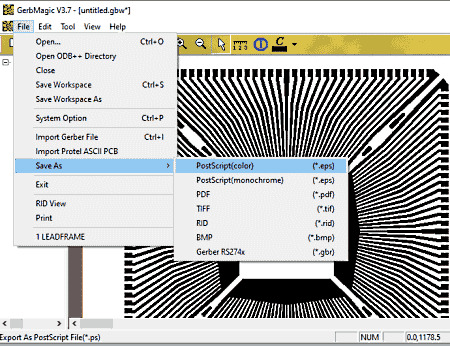
Altium designer 18 free gerber viewer

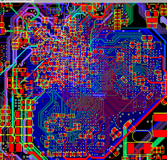
One question that you'll often see asked on forums around the internet is how to reverse engineer, or reconstruct, a PCB layout in a CAD program from a Gerber file. Learn more about Gerber viewer utilities and comparing Gerber files.More specialized CAM software specifically for Gerber files can be used to perform a variety of DFM checks that mostly involve clearances these will then get reported to you for any required updates before proceeding to PCB fabrication. This is the view manufacturers will use to initially inspect your board before providing a quote. In this view, we can clearly see that the Gerber viewer's role is to recreate a view of the PCB layout as you might view it in your ECAD software. The graphical view for this simple PCB layout was constructed from a set of Gerber files. If you put all the layers together and stack them on top of each other in a combined view with a Gerber viewer application, you'll get something that looks like the simple example shown below. XY coordinate locations for draw and flash commands Gerber file data is stored in an ASCII text file and it includes the following four elements: In terms of the data that gets stored in a Gerber file, the data in a Gerber file is human-readable, although not necessarily human interpretable. In some cases, such as creating drill drawings or fabrication drawings, multiple layers can be merged into a single file by mirroring mechanical layers into your Gerber outputs. The idea is that individual layers can be used to prepare stencils for each step in the fabrication and assembly process. Gerber files store all of the shape and location data for every element in a printed circuit board layout. In general, each layer in your PCB layout data will be placed into its own Gerber file. This front-end task in the PCB fabrication process is done with Gerber files. Somehow, those graphical images need to be reformatted into data that the PCB manufacturing company can use to create the a bare circuit board. When you design a printed circuit board on a CAD system, you will see all the different materials and elements on the board represented with different styles of lines and shapes.
Gerber Files: The First Step in the PCB Fabrication Process So what are Gerber files and what exactly do they communicate? We'll look at some examples of Gerber data in text and graphical format, as well as how this information is used in the PCB fabrication process by a manufacturer. Other available design output file formats are ODB++ and IPC-2581. Today, there are multiple options for output files you can generate for your design, but overwhelmingly, your project will likely use the Gerber file format. The answer is simple: generate output files in an appropriate format. How exactly do you translate your layout data from your CAD system into manufacturing instructions.
Perspective - choose this option for a more realistic view of the Multi-board Assembly.All of the pads and traces in your PCB layout will eventually need to be fabricated.
Orthographic - choose this option to see the exact position of objects and text on the Multi-board Assembly without being obscured by surrounding objects.
Projection – determine the projection of the view. Refer to the View Configuration panel page to learn more about the setting the color. Click the colored box to open a custom color drop-down to select a color for the associated object.
Toggle the / to show/hide the associated object.
This page is accessed by clicking View Configuration under the Multi-board Assembly folder in the main Preferences dialog (accessed by clicking the button in the top right corner of the workspace). The same set of options is available in the Multi-board Assembly View Configuration panel, use these to configure the settings in an open multi-board assembly. The Multi-board Assembly - View Configuration page of the Preferences dialog is used to configure the default system colors and display options of a Multi-board assembly. The Multi-board Assembly - View Configuration page of the Preferences dialog Summary Parent page: Multi-board Assembly Preferences
0 notes
Text
Shock Sensors Market Have High Growth But May Foresee Even Higher Value
Stay up-to-date and exploit latest trends of Shock Sensors Market with latest edition released by AMA. Keep yourself up-to-date with latest market trends and changing dynamics due to COVID Impact and Economic Slowdown globally. Maintain a competitive edge by sizing up with available business opportunity in Shock Sensors Market various segments and emerging territory. A shock sensor is detecting the shockwaves that are associated with a window or a door being broken. The shock sensor will be activated when a large shock wave is detected, and it sends an alert to the alarm system to let it know about the situation. Shock sensors Market is expected to grow in the future due to rising oil and gas explorations in the Middle East area and an increase in the number of smart home solutions. The multiple uses of these sensors in the consumer electronics segment are boosting the demand for shock sensors in the forecasted period.
Global Shock Sensors Market Report from AMA Research highlights deep analysis on market characteristics, sizing, estimates and growth by segmentation, regional breakdowns & country along with competitive landscape, players market shares, and strategies that are key in the market. The exploration provides a 360° view and insights, highlighting major outcomes of the industry. These insights help the business decision-makers to formulate better business plans and make informed decisions to improved profitability. In addition, the study helps venture or private players in understanding the companies in more detail to make better informed decisions. Major Players in This Report Include, Dytran Instruments Inc. (United States) , TE Connectivity (Switzerland), Metrix Instrument Co., (United States) , Emerson Electric Co. (United States), Murata Manufacturing Co., Ltd. (Japan), PCB Piezotronics Inc (United States) , Honeywell International, Inc. (United States) , Climax Technology Co., Ltd (Taiwan), Mobitron AB (Sweden).
Free Sample Report + All Related Graphs & Charts @: https://www.advancemarketanalytics.com/sample-report/5435-global-shock-sensors-market-1
Market Drivers High Demand for Shock Sensors in the Consumer Electronics Segment
Increasing Usage of Sensors in Goods and Manufacturing Plants Transportation
Rise in Number of Incidents of Theft Market Trend Restraints Proper Mounting of a Shock Sensor Challenges Shock Sensor Design Challenges Global Shock Sensors Market Report offers a detailed overview of this market and discusses the dominant factors affecting the growth of the market. The impact of Porter's five armies on the market over the next few years has been discussed for a long time in this study. We will also forecast global market size and market outlook over the next few years. Types of Products, Applications and Global Shock Sensors Market Report Geographical Scope taken as the Main Parameter for Market Analysis. This Research Report Conducts an assessment of the industry chain supporting this market. It also provides accurate information on various aspects of this market, such as production capacity, available production capacity utilization, industrial policies affecting the manufacturing chain and market growth. In this research study, the prime factors that are impelling the growth of the Global Shock Sensors market report have been studied thoroughly in a bid to estimate the overall value and the size of this market by the end of the forecast period. The impact of the driving forces, limitations, challenges, and opportunities has been examined extensively. The key trends that manage the interest of the customers have also been interpreted accurately for the benefit of the readers. The Shock Sensors market study is being classified by Type, Applications and major geographies with country level break-up that includes South America (Brazil, Argentina, Rest of South America), Asia Pacific (China, Japan, India, South Korea, Taiwan, Australia, Rest of Asia-Pacific), Europe (Germany, France, Italy, United Kingdom, Netherlands, Rest of Europe), MEA (Middle East, Africa), North America (United States, Canada, Mexico). The report concludes with in-depth details on the business operations and financial structure of leading vendors in the Global Shock Sensors market report, Overview of Key trends in the past and present are in reports that are reported to be beneficial for companies looking for venture businesses in this market. Information about the various marketing channels and well-known distributors in this market was also provided here. This study serves as a rich guide for established players and new players in this market. Current Scenario Analysis for Decision Framework Key Strategic Developments in Shock Sensors Market: The research includes the key strategic activities such as Research & Development (R&D) initiatives, Merger & Acquisition (M&A) completed, agreements, new launches, collaborations, partnerships & (JV) Joint ventures, and regional growth of the key competitors operating in the market at global and regional scale to overcome current slowdown due to COVID-19. Key Market Features in Global Shock Sensors Market The report highlights Shock Sensors market features, including revenue size, weighted average regional price, capacity utilization rate, production rate, gross margins, consumption, import & export, demand & supply, cost bench-marking in Shock Sensors, market share and annualized growth rate (Y-o-Y) and Periodic CAGR. Extracts from Table of Contents Chapter 1: Shock Sensors Market Overview Chapter 2: Global Shock Sensors Market Share and Market Overview Chapter 3: Shock Sensors Market Manufacturers/Players Analysis 3.1 Market Concentration Rate 3.2 Competition Scenario: BCG Matrix [Relative Market Share v/s Revenue Growth Rate] 3.3 Heat Map Analysis 3.4 FPNV Positioning Matrix 3.5 Comparative Market Share Analysis by Players (2018-2019) Rank, [% Market Share, Market Revenue] 3.6 Company Profile - Business Distribution by Region, Interview Record, Business Profile, Product/Service Specification, Price, Revenue and Gross profit 2017-2019 3.7 Price Benchmarking (2017-2019) Chapter 4: Global Shock Sensors Market Segmentation (Country Level Breakdown) (2014-2025)
North America: United States, Canada, and Mexico.
South & Central America: Argentina, Chile, and Brazil.
Middle East & Africa: Saudi Arabia, UAE, Turkey, Egypt and South Africa.
Europe: United Kingdom, France, Italy, Germany, Spain, Belgium, Netherlands, Poland and Russia.
Asia-Pacific: India, China, Japan, South Korea, Indonesia, Singapore, and Australia.
Chapter 5: Global Shock Sensors Market Breakdown by Segments (by Type (Piezoelectric, Piezoresistive, Capacitors, Strain Gage), Application (Aerospace, Automobile, Consumer Electronics, Medical Care, Others), Distribution Channel (Online, Offline), Material (Quartz, Tourmaline, Gallium Phosphate, Others)) 5.1 Global Shock Sensors Market Segmentation (Product Type) Market Size 2014-2025 5.2 Different Shock Sensors Price Analysis by Product Type (2014-2025) 5.3 Global Shock Sensors Market Segmentation (Product Type) Analysis 5.4 Global Shock Sensors Market by Application/End users Market Size 2014-2025 5.5 Global Shock Sensors Market Segmentation (other segments) Analysis Chapter 6: Methodology/Research Approach, Data Source, Disclaimer Buy the Latest Detailed Report @ https://www.advancemarketanalytics.com/buy-now?format=1&report=5435 This report also analyzes the regulatory framework of the Global Markets Shock Sensors Market Report to inform stakeholders about the various norms, regulations, this can have an impact. It also collects in-depth information from the detailed primary and secondary research techniques analyzed using the most efficient analysis tools. Based on the statistics gained from this systematic study, market research provides estimates for market participants and readers. About Author: Advance Market Analytics is Global leaders of Market Research Industry provides the quantified B2B research to Fortune 500 companies on high growth emerging opportunities which will impact more than 80% of worldwide companies' revenues. Our Analyst is tracking high growth study with detailed statistical and in-depth analysis of market trends & dynamics that provide a complete overview of the industry. We follow an extensive research methodology coupled with critical insights related industry factors and market forces to generate the best value for our clients. We Provides reliable primary and secondary data sources, our analysts and consultants derive informative and usable data suited for our clients business needs. The research study enable clients to meet varied market objectives a from global footprint expansion to supply chain optimization and from competitor profiling to M&As.
0 notes
Text
Which Files Are Required In PCB Layout?
1. Schematics (Necessary)
Whether it is drawn by hand or drawn by CAD, in short, only got Schematics can start PCB Layout;
2. The circuit power consumption calculation sheet (Unnecessary)
There are data about the power supply voltage and the current flowing through every single component. Without this, you need to interpret the Schematics to design the trace width and trace spacing.
In the absence of special software, free software such as LTspice can be used for circuit simulation.
In addition, verify through written calculations, and record the voltage value, positive and negative, current value and direction of flow for the places you need to check in the future.
The application in circuit board design is to calculate the width of the trace based on the current flowing through a certain area, especially for voltage traces and GND traces so that it can be used as a basis for designing connections the size and number of holes.
3. The electrical list of the Schematics (Unnecessary)
If no electrical list of the Schematics, which is able to make by yourself in the light of the Schematics. After all, the circuit electrical list is necessary for circuit board design.
Bt the way, the electrical network list for the circuit board is divided into a circuit diagram electrical network list and a circuit board electrical network list.
In many cases, especially when the circuit board is revised, the electrical network list will not be given. At this time, you need to do it yourself.
4. Bill of Materials (BOM) (Necessary)
Here to compare the consistency of the Schematics and the BOM. And mainly two reasons causing the inconsistency:
1>Constant changing when designing new products;
2>Components are eliminated or updated when the product is revised;
Therefore, no matter how much time it takes, the Schematics must be consistent with the component list to ensure the success rate of the PCB Layout.

5. Circuit board design drawings (Necessary)
Even scribbled handwriting is still terribly necessary. If it is only delivered verbally, which will be possible lead to errors due to misunderstand the meaning of the product designer.
The content of the drawing: Board, surface treatment, the minimum limit of trace width and trace spacing, the specifications of the pads, the font and size of the printing.
The size of the circuit board, the location where the specified component is placed, and the prohibited area. Insulation specifications between different areas, etc.
6. Circuit board layout schedule
Calculate how long the circuit board layout takes, and how many layout engineers requries.
7. Circuit board area estimation table
Within the specified circuit board size, judge whether the components can be reasonably arranged in the circuit board.
In the case that the components can be arranged in the circuit board, it is judged whether to adopt a two-layer design, four-layer design or more.
Apart from that, in the absence of any designation, it is also necessary to fully communicate with the product designer to recommend the most appropriate circuit board size and layer design.
8. Workpiece size estimation table
After determining the size of the circuit board, in order to achieve the minimum production cost in production, several individual circuit boards will be connected together by V-cutting. At this time, the appropriate workpiece size must be selected.
9. Circuit board electrical design table
It includes the following parts:
1>Trace width calculation table or trace width reference table;
2>Trace spacing calculation table or trace spacing reference table;
3>Connection hole pads size calculation table or Connection hole pads size reference table.
https://www.grande-pcba.com/

0 notes
Photo

$39.25 33% off sell - 4.94m 150 LEDs RGB Colorful Dimmable Flat LED Strip Light - Black - 3129605113 Brief Introduction: Feel that cool white and warm white light in your house is a little dull? Or want to add some festival atmosphere to your house? This flexible LED strip is perfect for nearly any applications including mood and accent lighting. It will produce colorful light while being very energy efficient. And this LED ribbon is also a cool and efficient way to decorate tables, shelves, entertainment rooms, kitchens, bedrooms, closets, etc. Main Features: - Adopted 150pcs high-intensity LEDs and premium PCB component, low power consumption, safe to use- RF remote control (not included), 15m remote distance- Various lighting effect, which is vivid and beautiful- 4.94 meters string lamp consists of 150 LEDs- Extra durable and flexible strap, easy to shape as you like- IP67 waterproof, ideal for indoor and outdoor use- Ideal for architectural lighting, concealed lighting, perimeter lighting and many other applicationsParameters: - Material: rubber + FPC board- Power: 22 - 23W- Length: 4.94m- LED: 150pcs SMD5050 RGB- Output Voltage: 5VNote: - The LED lighting effects must be switched by the remote control- Installation surface must be smooth, clean and dry- The part of LED components can not be fixed on the surface of sharp edge- Strip should not be collided or crushed- Strip can be cut following the cutting lines- The LED strip must not exceed 5m when used in a DC series circuit Average Life (hrs): 80000 hours Occasion: Bedroom,Garden,Living Room Power Source: DC Strip type: SMD 0.204 Package weight: 0.238 kg Package Size(L x W x H): 24.00 x 22.00 x 2.00 cm / 9.45 x 8.66 x 0.79 inches Package Contents: 1 x Flat LED Strip Light, 1 x Connection Head (0.1m), 1 x Wire Coil IPXX Rating ChartIP Code The IP Code (or International Protection Rating, sometimes also interpreted as Ingress Protection Rating*) consists of the letters IP followed by two digits and an optional letter. As defined in international standard IEC 60529, it classifies the degrees of protection provided against the intrusion of solid objects (including body parts like hands and fingers), dust, accidental contact, and water in electrical enclosures. The standard aims to provide users more detailed information than vague marketing terms such as waterproof.The digits (characteristic numerals) indicate conformity with the conditions summarized in the tables below. For example, an electrical socket rated IP22 is protected against insertion of fingers and will not be damaged or become unsafe during a specified test in which it is exposed to vertically or nearly vertically dripping water. IP22 or 2X are typical minimum requirements for the design of electrical accessories for indoor use. more product select from our Strip Lights:https://www.gardennero.com/1271-strip-lights #& # # .94m # #
#StripLights#Lights#Lighting#Indoor#Strip#4#150#LEDs#RGB#Colorful#Dimmable#Flat#LED#Light#Black#3129605113
0 notes
Text
What is a capacitive switch?
A capacitive switch is an electronic capacitor that measures changes in capacitance values when a conductive object such as your finger moves closer to the sensing area. The change in that value is interpreted and registers that change as an activation of the switch. A capacitive switch can be either a flexible printed circuit or a sensing pad on a rigid PCB. A capacitive switch can incorporate a lot of functionality that is not easily attained with a normal membrane or mechanical switch. Capacitive switches can have intensity sliders, sensitive areas in multiple shapes such as a circle, and can have varying levels of sensitivity for activation. You also can have options like a proximity sensor incorporated into a capacitive switch for additional functional benefits. As a capacitive switch is a sensor that senses through a non-conductive surface, thicker substrates can be used such as safety glass, or acrylic materials for a very robust switch. This can also give the ability for additional gasketing for harsh environments. It is also possible to achieve very intricate backlighting solutions with capacitive switch technologies.

0 notes
Text
New Ruling On CERCLA Will Force Corporations To Think Twice About Polluting
By Rosaura Ritger, American University Class of 2021
September 10, 2020

The Comprehensive Environmental Response, Compensation, and Liability Act (CERCLA) is a federal law that provides a ‘Superfund’ for environmental clean of hazardous and toxic waste that is not controlled or has been abandoned. Power was given to the US Environmental Protection Agency (EPA) to hold parties accountable in the cleanup process and ensure their cooperation.[1]
On August 12th, 2020, there was a ruling clarifying the interpretation of CERCLA and its statute of limitations for liability in environmental cleanup with plaintiff MPM Silicones LLC and defendant Union Carbide Corporation (UCC) as parties. The problem goes back to the 1960’s where UCC conducted its manufacturing on a site in Friendly, West Virginia that borders the Ohio River. [2] UCC manufactured an array of chemical products beginning in the mid ‘50s which generated substantial amounts of chemical waste until it sold the site in the ‘90s. Among the chemical waste were toxins known as polychlorinated biphenyl (PCB).[3]
In 1972, around the same time that the use of PCB’s in manufacturing was banned, the site raised concerns about their chemical waste and the methods used to dispose of it. UCC stopped using PCB’s in manufacturing at that time, however, a few years later soil tests showed evidence of PCB presence. UCC began to reexamine its waste management methods and conducted more testing across its 1900-acre site for the next few years.
The testing focused on several chemicals including the PCBs, however, the samples showed low levels of PCBs and were inconsistent according to the statements made in the case digest summary.[2]A memorandum was issued in response to the tests stating there was ‘no definitive evidence’ for the amount of PCBs speculated to be buried at the site.
In 1981, as required by the Resource Conservation and Recovery Act (RCRA), UCC submitted a permit to the Environmental Protection Agency (EPA) to treat and dispose of their chemical waste.[4] However, while filling out the permit, UCC did not disclose its prior use of PCBs on the document to the EPA and characterized their soil analyses results as negligible in regard to PCB presence. As a result, the EPA workplan for UCC did not include any plans for PCB cleanup.
In 1993, UCC made an agreement to sell the site to OSi Specialties, Inc. – now known as Crompton Corporation – where ‘environmental due diligence’ was conducted by a third-party organization prior to closing. The third-party organization requested information about UCC’s waste management and cleanup. UCC directed them to the workplan given by the EPA. Again, the presence of PCBs on the site was considered negligible and the tests done did not indicate a level high enough to call for cleanup as required by EPA regulations.
The site was sold again in 2003 to GE Advanced Materials – now known as Plaintiff MPM Silicones – where the same third-party organization was called in to perform an environmental assessment of the site. This third-party organization – Environment Strategies Corporation (ESC) – determined that the site had reached a PCB-free status by removing the PCB-containing machines from the site.
GE hired a different organization – ENVIRON – to conduct their own assessment, prior to the sale. In testimony, the GE employee that oversaw the assessment stated UCC had once again mentioned their PCB testing but that the results could not substantiate any proof of the chemical’s presence on the site. In addition to this, UCC related the possible presence of PCBs to their prior use of PCB containing electrical equipment which could have potentially leaked or spilled onto the site during maintenance. According to the same testimony, the GE employee noted that UCC did not mention their use of PCBs in the manufacturing process in addition to the PCB-containing electrical equipment. Upon results of ENVIRON’s soil and groundwater testing, significant amounts of PCBs were found in the samples taken in the testing which exceeded the EPA’s regulations. These results were seen as ‘unexpected’ to ENVIRON and GE, yet no further remediation actions were taken at this time.
In 2008, MPM Silicones (formerly GE) was upgrading a wastewater treatment unit when they discovered more PCB contaminated soil. They immediately halted the construction and spent over $120,000 in expenses to clean up and remedy the contaminated soil. MPM informed OSiCrompton of the contamination and claimed their liability, but OSi did not agree, citing the indemnity agreement in their purchase agreement. It is then noted that MPM hired another environmental consulting firm to conduct testing around the wastewater treatment unit site, incurring more costs for the remediation.
In 2010, MPM contacted UCC – the original owners of the site – about the PCB contamination because they were planning on resuming the construction of the new wastewater treatment unit, and to do so would require more cleanup. At this time MPM had found old documents from the 1970s about UCC’s usage of PCBs in their manufacturing and sought remediation payments.
The initial claim brought by MPM sought reimbursement for expenses of the cleanup of PCB contamination on the site in West Virginia that had previously been owned by UCC. In response, UCC filed a crossclaim that MPM should be liable for a portion of those expenses. This case was initially heard at the District Court for the Northern District of New York where MPM’s action to seek reimbursement for ‘remedial actions’ was granted a partial summary judgement because it was ‘time-barred’ under 42 U.S.C §9613(g)(2). UCC was held liable by this district court for 95% of future ‘removal actions’ on the site. Both parties appealed to the Circuit Court of Appeals.
The case was reviewed at the Second Circuit Court where it considered the district court’s interpretation of one of the circuit’s prior decisions in the NYSEG case.[5]The court held that the actions taken by MPM to replace a wastewater treatment unit were remedial in nature, and not characterized as a removal action, which meant that their claim for reimbursement was not time-barred. CERCLA defines ‘remedial’ and ‘removal’ actions:
“The terms "remove" or "removal" means 2 the cleanup or removal of released hazardous substances from the environment, such actions as may be necessary taken in the event of the threat of release of hazardous substances into the environment…”
“The terms "remedy" or "remedial action" means 2 those actions consistent with permanent remedy taken instead of or in addition to removal actions in the event of a release or threatened release of a hazardous substance into the environment, to prevent or minimize the release of hazardous substance…”[6]
It is also noted in the Circuit’s opinion that the District Court erred in their interpretation of the NYSEG case where they claimed that only one remedial action can occur at a site. The Circuit Court clarified their reasoning in the referenced NYSEG case as applied to the current case:
“For the reasons explained above, we understand the single-remediation principle stated in NYSEG to mean that,when a remediation is undertaken under a remediation plan based on full disclosure of the known problem,successive remedial steps undertaken in furtherance of the original objective are part of a single remediation for purpose of the statute of limitations, so that the remediator may not delay suit by classifying subsequent stages of remediation of the original problem as new remediations”[2]
Pursuant to the second claim by UCC, the Circuit affirmed the District court’s ruling that UCC is liable for future removal expenses at the site. The Court remanded for further proceedings to determine whether the remedial actions by MPM were of the same character of those initialized by UCC in the ‘80s, or if the actions were of a new character permitting MPM to seek reimbursement within a timely manner of the commencement of said remedial actions.
This ruling clarifies the NYSEG case decided by the Second Circuit Court regarding this ‘single-remediation principle’ when it comes to characterizing the action taken by a claimant in order to receive compensation under CERCLA. Polluting corporations (polluters) that have been using hazardous chemicals in manufacturing processes and do not disclose that usage in permits to the EPA under RCRA are now explicitly liable for remediation and removal actions taken to clean up the waste by any claimants who incur those costs as a direct result of their (the polluter’s) negligence.
________________________________________________________________
[1]Summary of the Comprehensive Environmental Response, Compensation, and Liability Act (Superfund). (2020, July 27). Retrieved from https://www.epa.gov/laws-regulations/summary-comprehensive-environmental-response-compensation-and-liability-act
[2] MPM Silicones LLCv. Union Carbide Corp. Court: U.S. Court of Appeals for the Second Circuit; Practice Area: Environmental Law; Case Number: 17-3468(L); Case Digest Summary. (2020). New York Law Journal,264(30), 17.
[3] Learn about Polychlorinated Biphenyls (PCBs). (2020, February 06). Retrieved from https://www.epa.gov/pcbs/learn-about-polychlorinated-biphenyls-pcbs
[4]Resource Conservation and Recovery Act (RCRA) Overview. (2020, May 26). Retrieved from https://www.epa.gov/rcra/resource-conservation-and-recovery-act-rcra-overview
[5] New York State Elec. & Gas v. FirstEnergy Corp., No. 11-4143 (2d Cir. 2014). (2020). Retrieved from https://law.justia.com/cases/federal/appellate-courts/ca2/11-4143/11-4143-2014-09-11.html
[6]42 USC Ch. 103—Comprehensive Environmental Response, Compensation, and Liability. (1980, December 11). Retrieved from https://uscode.house.gov/view.xhtml?path=/prelim@title42/chapter103
0 notes
Text
BiTipText enables text entry across two index finger-worn keyboards

Typing with your thumbs on a smartphone has become an everyday activity for many, but what if you could enter text by simply tapping on your index fingers? With BiTipText, that may soon be a reality.
The researchers’ prototype consists of an interactive skin overlay made out of flexible PCB material, allowing an Arduino Uno and MPR121 sensor chip to read capacitive signals from both digits.

In testing, users were able to enter text at over 23 WPM, with a 0.03% uncorrected error rate. Notably, the two-handed implementation means that software can determine not only the position of presses, but the sequence of left/right inputs to help with word interpretation.
More details on the bimanual text input method can be found in the team’s paper here.
youtube
BiTipText enables text entry across two index finger-worn keyboards was originally published on PlanetArduino
0 notes
Text
A Guide to Electronics Packaging Design


Electronics packaging design is the production and enclosures of electronic devices ranging from microchips up to full on electronic systems. Since electronic products are considered fragile, the electronics product packaging design must consider protection from extreme temperatures, mechanical damage, electrostatic discharge and high frequency noise emission. However, it should also be as simple as possible as Apple has demonstrated. The quality control team always sets high standards with respect to electronics packaging. In fact, some electronics manufacturing companies simply outsource from established electronic packaging companies who are already proven when it comes to creating custom electronic packaging. This solution will be helpful to the quality control team since they no longer have to worry about the electronic packaging aspect.

Fundamentals of Electronics Packaging
Electronic packaging is arguably the most complex among all levels of packaging as it requires extensive engineering and skill set in order to come up with an optimal overall electronics packaging design compared to other industry packaging designs. The wide range of options available makes it hard for the production team to decide since the choice may potentially conflict with the functions of the electronic packaging. The choice should also be consistent with traditional packaging design practices and manufacturing capabilities. As electronic packaging is built and tested, it can be expected multiple revisions are inevitable. The electronic packaging design will continuously be rethought and revised until the final packaging design is achieved.

Functions of an Electronics Packaging Design
The electronic packaging design is a combination of minor electronic packages working altogether to achieve desires purpose. They are not only present to protect the PCB and electronic components from outside harm but also make sure they do not interrupt with the functions of these components. Unpacking is more and more seen as an experience. Technological advancements also put a lot of pressure to electronic packaging companies because functions of the electronics packaging design evolve at a fast rate, keeping up with modern technology. The functions do not remain constant because as technology improves then the demands on electronic packaging also increases and change accordingly. One of the foremost drivers in the electronics packaging industry is the fast pace evolution of the silicon IC technology. Another crucial driver is continuous photonics development which is automatically integrated to the various level of media interconnections relative to custom electronic packaging. These drivers force electronic product packaging designs to adapt and modify electronic packaging’s functions. Speaking of photonic technologies, these electronic components are physically attached to the PCB elevating its design into an advanced form. Since they are physically interconnected with each other along with basic components of the system, this will stress pressure to the schematic design of electronics packaging.

Different Levels of Electronic Packaging
Electronics packaging design is organized in multiple levels namely Level 0 up to Level 5. Level 0 – this electronic packaging level protects chips and semiconductors which are the simplest and most basic parts of an electronic system. Level 1 – this electronic packaging level protects electronic components. Level 2 – this electronic packaging level protects the printed circuit board. Level 3 – this electronic packaging level protects assembly, wiring boards and associated components of these. Level 4 – this electronic packaging level protects modules or collection of assemblies. Level 5 – this electronic packaging level protects a combination of different modules or the electronic system in general. These levels are necessary to help electronic manufacturing companies easily assess electronic packaging materials needed for an electronic packaging design. This makes operations more efficient and fluid since they can easily look for what they need simply by describing the electronic packaging level they are currently working on.

Electronics Packaging Design and Engineering
Creating custom electronics packaging designs are focused on achieving objectives by covering these following qualifications: 1. Interpretation of Specifications Aside from the electrical circuits, the electronics packaging engineer should also be able to interpret the non-electrical concerns needed for the electronics packaging design. These non-electrical concerns are functionality, reliability, aesthetics, durability and production cost. Even if the electrical circuits are all in place yet the design failed any of these other concerns then the electronic product packaging design can still be considered failure to comply with standards. 2. Having a Design Approach Even if the electronic packaging engineer is equipped with the right skills and knowledge to create the custom electronic packaging, he or she still has to have a design approach in place to do the job. The right product design approach is needed to meet the requirements set on the electronic packaging design. 3. Cost-Efficiency If you are in the world of manufacturing, you should understand the importance of the ratio between cost and value. Having an electronic packaging design which is too expensive would offset its value even if it is fully-functional. The electronic design engineer must explore all options available with regards to electronic packaging foam and electronic packaging materials until the end result has a rational cost to value. Being cost-efficient is a key aspect of manufacturing not only in electronics. Product development with prototype companies can help. 4. Mechanical Knowledge Most electronic design companies seek help from mechanical engineers and not only rely with electrical experts when it comes to custom electronic packaging. Their knowledge and expertise could make up for the non-circuitry areas of the project to make sure all aspects are covered. Read the full article
0 notes