#PCB production
Text
Die fünf Hauptfunktionen von Lötstopp-Lochverschlüssen
1️⃣ Verhindern des Fließens von Lötzinn durch die Durchkontaktierungen und Vermeidung von Kurzschlüssen während des PCB-Wellenlötens, insbesondere wenn die Durchkontaktierungen auf BGA-Pads platziert sind. Es ist notwendig, die Löcher vor der Vergoldung zu verschließen, um das BGA-Löten zu erleichtern.
2️⃣ Vermeiden von Flussmittelrückständen innerhalb der Durchkontaktierungen.
3️⃣ Nach der Oberflächenmontage und Bauteilplatzierung muss die Leiterplatte auf einer Testmaschine einem Vakuumsaugtest unterzogen werden, um einen Unterdruck für die Fertigstellung zu erzeugen.
4️⃣ Verhindern des Fließens von Lötpaste in die Löcher und Vermeidung von Lötfehlern, die die Lötung während der Montage beeinträchtigen könnten.
5️⃣ Verhindern des Herausspringens von Lötkugeln während des Wellenlötens, was zu Kurzschlüssen führen könnte.

2 notes
·
View notes
Text
Cost-Effective Strategies for Efficient PCB Production by A-Gas Electronic Materials
Learn how to optimise PCB production with cost-effective strategies, including design for manufacturability, efficient production techniques, and energy efficiency. Improve quality and reduce costs. Contact A-Gas Electronic Materials for expert guidance and tailored solutions.
#PCB production#cost-effective PCB manufacturing#design for manufacturability#PCB materials#efficient PCB production#supplier collaboration#PCB inventory management#PCB energy efficiency#automated assembly#A-Gas Electronic Materials#UK#PCB production strategies#PCB quality improvement
0 notes
Text
#pcb design#pcb factory#pcb manufacturer#pcb production#pcb prototype#pcb supplier#pcb fabrication#pcb reverse engineering
0 notes
Text
Ensure PCBs for automotive applications meet high reliability standards. Optimise layout, consider EMI/EMC, use robust materials, and perform thorough testing. In the evolving landscape of automotive engineering, printed circuit boards (PCBs) are the backbone that power the intricate systems within advanced modern vehicles. With the rapid research and development of the autonomous vehicle segment, the importance of PCB design in this field has reached new dimensions. Modern cars rely heavily on printed circuit boards, which act as a central nervous system coordinating many operations, including engine control, sensor systems, and safety measures.
0 notes
Text
#pcb assembly services#circuit board assembly#printed circuit assembly#printed circuit board design#electronic pcb#pcb fabrication and assembly#pcb production#pcb design service#pcb fabrication#pcb electronic#oem electronics manufacturing#pcb prototype us
0 notes
Video
undefined
tumblr
WaifuPad Startup animation and a chime
#waifupad#waifu#macropad#diy#electronics#adobe illustrator#illustrator#macro#soldering#pcb#controller#device#productivity#vector graphics#usb#shortcut#keystroke#arduino
98 notes
·
View notes
Text
Enhance Efficiency and Flexibility with DIN Rail Mounted Terminal Blocks in India
Introduction:
In today's rapidly evolving industrial landscape, efficient and reliable electrical connections are crucial for ensuring smooth operations. DIN rail mounted terminal blocks have emerged as a preferred solution for creating secure and organized electrical connections in a wide range of applications. With their versatility, durability, and ease of installation, these terminal blocks have gained immense popularity among professionals in India. In this blog post, we will explore the benefits and applications of rail mounted terminal blocks and highlight their importance in the Indian industrial sector.
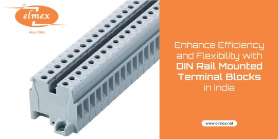
What are DIN Rail Mounted Terminal Blocks?
DIN rail mounted terminal blocks are electrical connectors that provide a convenient and standardized method for connecting and distributing power or signals in industrial control systems. These blocks are specifically designed to be mounted on DIN rails, which are widely used for organizing and securing electrical components in control panels, switchgear cabinets, and equipment enclosures.
Benefits of DIN Rail Mounted Terminal Blocks:
Space-saving and Modular Design: DIN rail mounted terminal blocks feature a compact design that allows for optimal use of available space. Their modular construction enables easy customization and expansion as per the specific requirements of an application, making them highly adaptable.
Secure and Reliable Connections: These terminal blocks ensure secure and reliable connections, thanks to their robust construction and advanced connection technologies. They provide a sturdy grip on wires and facilitate excellent contact, minimizing the risk of loose connections and electrical failures.
Easy Installation and Maintenance: With their tool-less and user-friendly design, DIN rail mounted terminal blocks simplify installation and maintenance procedures. The snap-on mounting feature of these blocks allows for quick and hassle-free assembly, reducing overall downtime during system installation or upgrades.
Enhanced Safety: Rail mounted terminal blocks adhere to stringent safety standards and offer features like finger-safe design, which prevents accidental contact with live components. This ensures the safety of both the equipment and the personnel working with them.
Applications of DIN Rail Mounted Terminal Blocks:
Industrial Automation: Rail mounted terminal blocks are extensively used in industrial automation systems, where they serve as a vital component for connecting sensors, actuators, motors, and other devices. These blocks provide a reliable interface for transmitting power and signals between various control elements.
Power Distribution: DIN rail mounted terminal blocks play a crucial role in power distribution systems, allowing for easy and organized connection of power supply lines to different equipment. They enable efficient energy management and facilitate the distribution of power to multiple devices within a control panel.
Building Automation: In building automation systems, DIN rail mounted terminal blocks provide a convenient solution for connecting various electrical components, such as lighting controls, HVAC systems, security systems, and more. Their modular design allows for easy integration and maintenance of these systems.
Rail Mounted Terminal Blocks in India:
The Indian industrial sector is witnessing significant growth, and the demand for reliable electrical connectivity solutions is higher than ever. Rail mounted terminal blocks have gained traction in India due to their versatility and ability to meet the diverse requirements of industries ranging from manufacturing to infrastructure development. Manufacturers and suppliers in India offer a wide range of DIN rail mounted terminal blocks, catering to different voltage and current ratings, wire sizes, and connection types.

Conclusion:
Rail mounted terminal blocks have revolutionized the electrical connectivity landscape in India, providing efficient, secure, and organized solutions for various industrial applications. Their space-saving design, ease of installation, and robust construction make them indispensable for creating reliable connections in control systems and power distribution networks. As the industrial sector continues to thrive in India, the importance of DIN rail mounted terminal blocks as a key component in electrical installations cannot be overstated. By embracing these advanced terminal blocks, Indian industries can enhance efficiency, reduce downtime, and ensure safe and reliable operations.
#Rail Mounted Terminal Blocks India#DIN Rail Mounted Terminal Blocks India#Power BusBar Terminal#Finger Safe Power Terminal blocks#Barrier Terminal Block Manufacturer in India#electrical wire termination technology#manufacturer#terminal block#DIN Rail Mounted Connectors#switchgear industry#solar product#PCB connectors#DIN rails channels#digital voltmeter#digital ammeter#power and signal#current transformer#railway#renewable energy#elmex#electrical company#electrical industry
2 notes
·
View notes
Text
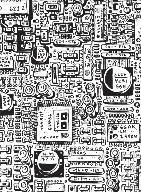
Wizzywig
Ed Piskor
#comics#comic books#art#illustration#panelswithoutpeople#b&w#black and white#graphic novel#graphic novels#Wizzywig#Ed Piskor#tech#Circut board#PCB#computer#computers#top shelf productions#top shelf
0 notes
Text
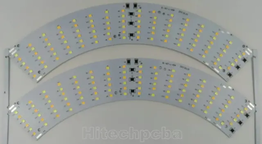
LED PCB Assembly
What is the LED Circuit Board assembly?
Generally, LED PCB assembly is considered to be a circuit board that has the LED components soldered to it. The LED is soldered to the printed circuit board and features a chip that creates the light as electrically connected. A thermal heat sink and a ceramic base are used to bond the chip. Not all the PCB products can be used in Led industry, as an LED PCB is easy to create a high volume of heat, but making it hard to cool with traditional methods. For this reason, metal core PCB is widely used in LED application because of their enhanced ability to dissipate heat, especially aluminum pcb is often used to fabricate PCB for LED lights.
We’ve had great LED PCB assembly experiences with top LED chips to brand such as Cree, Luxeon, Osram, Nichia, Lumileds, MLS, EVERLIGHT, Samsung, LG, Seoul., etc. PCB LED lights can be incorporated into numerous lighting applications due to their combination of excellent energy efficiency, low cost and maximum design flexibility.

Application of LED PCB Assembly
Hitechpcba serves customers in different industries, providing highly reliable and innovative LED PCBs for various applications:
• Horticulture light LED PCB Assembly
• LED controller PCB Assembly
• Computer LED display and indicators
• LED lights PCB Assembly for medical use
• Automotive LED PCBs Assembly include PCBs for brake lights and headlights
• Street lighting LED PCB Assembly
• Flashlights and camping accessories
• Traffic light PCB Assembly
• Commercial lighting LED PCB Assembly
LED PCB Assembly specification
Number of layers for LED PCB
These layers are made up of aluminum and magnesium, but now have Copper base material and Ceramic base materials for LED PCB industry, we can meet it.
Aluminum LED PCBs stand out among other PCBs because it has a good insulation characteristic and has a better machinery performance, the cheap cost is one important factor too.
Types of layers for LED PCB Assembly
Normally, the base layer is made using aluminum alloy metal.
This aluminum alloy substrate used in making the base makes it ideal for through-hole technology which transfers and dissipates heat.
A thermal insulation layer is made using some ceramic polymer which has good viscoelasticity characteristics.
It is highly heat resistant and protects the PCB against heat and mechanical stress.
The circuit layer, which is covered by a copper foil which can range from one to ten ounces.
LED Board type- single or in panel
Some boards are shapeless. For this reason, LED PCB panels are used. This reduces time, labor production and testing time.
Some LED PCB Assembly is done on a single board while others are done on panel boards.
LED PCB Assembly Process
Roughly, the PCBA process can be divided into theses phases: soldering paste printing > SMT (surface mounted technology) > reflow soldering > AOI (automated optical inspection)> THT (through-hole technology) > wave soldering > touch-up and cleaning > IC-programming > FCT (functional tests) > aging testing.
Below we show you the process.
Step1. Summarizing Project Information
Before contacting your supplier, make sure you have all the project information. Suppliers will need info following for quoting LED PCB assembly:
Gerber
BOM
LED PCB specification
Quotation quantity
Once you have gathered these information, you can contact us and request for a quote.
Of course, you can also provide the schematic, LED PCB Assembly pictures and even samples to us. The more details they have, the more accurate the supplier’s quotation will be.
Step2. Discussion and details about custom LED PCB Assembly
Different projects will have different requirements. Remember the special requirements mentioned in step 1? That’s going to be the focus of this session. Equipment and engineering capacity will not be identical between suppliers. Make sure your supplier has the equipment to produce and assemble major components and the corresponding testing capabilities.
For example, some vendors don’t have X-ray testing equipment, which means they can’t check the mount quality of BGA chips. Outsourcing this step will increase risk and cost. That’s what you don’t want.
Also, pay attention to time taken by the supplier to quote. Motherboards often contain hundreds or even thousands of components, and they are supplied by different manufacturers. To ensure the quality of the components, the supplier sourcing team will make multi-inquiries from these manufacturers or authorized suppliers to match customer’s requirement, which usually takes 2-3 business days, and even longer for some scarce chips. Therefore, if your project is complex and the supplier quotes you within few hours, double check with them.
Step3. Sample and feedback
After confirming the PI, the supplier will usually provide pre-production samples for your approval. At the same time, the supplier will also confirm with you the logistics plan of the bulk goods. Make sure they understand your shipping requirements, including details on packaging, customs clearance, taxes, etc.
For us to have a successful LED PCB Assembly process, its functions must be defined. Compliance requirement is defined to reduce the effect when components are selected.
The Bill of Materials is then generated from the information installed on the LED PCB.
All this information is used to assemble components which are identified from MOB to the LED PCB.
After that, the routing of traces is determined to each component, based on the size, shape of the circuit board and location of connectors.

Hitech Circuits is trusted by thousands of electronic engineers on their LED PCB assembly projects, from consumer, led bulb to precisely medical LED light, we can help you from the beginning of design stage; From commercial flood LED to industrial high power LED, from automotive LED to military LED, Venture is the perfect place for your LED PCB assembly requirement.
Hitech Circuits has been participated in hundreds and thousands of LED lighting projects, by providing LED PCB and also LED PCB assembly service.
Our LED PCB assembly had covered both ends of the Lighting Class LED size spectrum, assembling some of the largest (2 meter long boards) and some of the smallest LED Lighting applications which used in Medical Endoscopes.
LED PCB Assembly is very crucial in the current industrial development. Many electrical devises are being innovated and the old once being improved.
LED PCBs are useful due to the fact that they are made using materials that can transfer and dissipate heat. This characteristic increases device durability.
The world is changing with new technology, especially PCB technology that plays an essential role in the application of LED circuits. And the LED industry is taking advantage of this technology and growing faster.
As a full feature PCB solutions provider with more than a decade of experience, we're capable to provide LED PCB fabrication, components procurement and LED PCB assembly all under one roof. We can work with you to develop metal core PCB, aluminum circuit boards customized to your specific applications. We feature competitively priced PCBs made with standard FR-4 material that includes a thermal aluminum clad layer that will efficiently dissipate heat, keep all LED PCB components cool and significantly enhance the performance of your products.

LED pcb board, LED pcb assembly
LED with its advantages of high brightness, high efficiency, low heat, long life, is considered the most development potential in the 21st century lighting. In the market and policy driven by the rapid development of the domestic LED industry blowout has formed a relatively complete industrial chain, including the production of epitaxial wafers, chip preparation, packaging, integration, LED application. In 2010, China's LED industry scale, up from $ 827 billion in 2019 to 220 billion yuan, an annual growth rate of over 70%, higher than the 50% level of growth of the global LED lighting industry output value. Among them, the middle and lower reaches of the most complete industrial chain, accounting for 90% of the overall percentage of the GDP.Chinahas become the world's leading LED manufacturing base and important application market.
To further promote the technological innovation of the LED industry, construction and wide application of independent industry chain, China Electronic Appliance Corporation and industry associations to organize the theme of "Focus on the core energy LED Exhibition will be held November 9-11, 2010 in Shanghai International Expo Center and the 78th China Electronics Fair over the same period will be held will create from raw materials, epitaxial wafers, chip, LED bracket, LED accessories, LED packaging and supporting materials, the LED backlight upstream firm to the upstream and downstream enterprises of the display, lighting, landscaping, decorative lighting, traffic lights, automotive lighting, special lighting, to the equipment, instrumentation, software, finance, consulting and other service enterprises and technological exchanges and market trading platform, help the domestic industry sustained and healthy development, and promote the steady expansion of the LED application market.
In the LED industry chain upstream of the epitaxial wafers and LED chips accounted for 70% of the profits of the whole industry, and technology-intensive, capital-intensive, where the core technology of the LED. Well-known epitaxial wafer and chip production enterprises will be exhibited a number of energy-efficient, low heat, cost-effective LED products, many of whom have excellent products of international advanced level.
LED electronic pcb assembly manufacturing 100% Original LED Chip with one-stop in-house pcba services
3 notes
·
View notes
Text
Discover A-Gas Electronic Materials' EIF solutions for high-performance PCB production and electronic components. Our advanced chemistries ensure superior quality and reliability in electronic devices. Trust A-Gas for innovative industrial finishing technologies.
#Electronic Industrial Finishing#EIF solutions#high-performance PCBs#electronic components#plating solutions#metal stripping#cleaning agents#soldermask resists#A-Gas Electronic Materials#UK electronic manufacturing#electronic finishing services#PCB production#electroplating#metal treatment products
1 note
·
View note
Text
https://www.futureelectronics.com/p/production-products--hardware--test-points/5015-keystone-8064685
PC hardware monitor, Security testing, PCB Test Point, Hardware test plan
Miniature Surface Mount Test Points on Tape and Reel
#Keystone#5015#Production Products#Hardware Test Points#pc hardware monitor#Security testing#PCB#plan#acceptance testing#Hardware testing process#open hardware monitor#software#development process#Hardware testing tools
1 note
·
View note
Text
How Is Pcb Prototyping Different From Full Spec Production?
In an era that significantly promotes innovations and advancement of technology, we're looking at constant growth in the usage of PCBs. The lesser turnaround time of production has revolutionized the way R & D departments function. We are well aware of this change and hence we optimize our operations likewise, be it production, or delivery.
The quantum of production of PCBs is always fluctuating, on the basis of orders. Based on that, there are two different production standards- Full Spec Standard PCB Production & PCB Prototyping.
Both these processes work at their own pace and are preferred based on the end requirement. In the first stage, a design is created, and prepared on a board layout; then it is tested on a prototype level. The initial testing stages can be helpful in experimenting with the various designs from multiple aspects and then it can be converted into a sophisticated final product that is ready to use.
To conclude; getting rid of the errors and flaws before a prominent expense seems much more beneficial.
Let's circle back to why PCB Prototyping is recommended and why it is often preferred by designers and innovators.
What are the benefits of PCB Prototyping?
Prototyping has proven to be the best practice before you go ahead for full spec production as it gives more room for experimenting to develop the desired output.
Prototyping helps customers make advancements on existing designs.
When there are no conjectures involved, the timelines are exponentially cut down and there is a turn for the better when it comes to turn-around time.
Prototyping makes it easier for you to determine accuracy and performance and hence, there is a scope for significant improvement at every stage which helps an innovator make the best version of their end product.
Prototyping reduces redundant practices. The process of prototyping aids in multiple aspects like patent drawings, inventor's logbook, etc. which is instrumental in making the patent filing significantly easy.
A prototype is instrumental in helping you create a functioning beta product that can help you acquire funds for large-scale manufacturing.
Any advancement done to the initial design may have defects, flaws, inconsistencies, and challenges. All these can be minimized before a full-fledged production comes into action. With prototyping, comes a scope of making multiple iterations for the best possible results.
Post the prototyping phase comes the full spec production.
Prototyping in the early stages will always help you define your results better and it will also help determine the efficacy.
Designers can then move on to working on the design at scale, providing greater flexibility to refine and optimize the functionality of the product.
But, are there scenarios when you go for a full spec production before the prototype stage?
The answer is yes. There are a few situations and scenarios wherein it is recommended to do so; like:
If there are multiple components involved and the project is composite
If there is the involvement of innovation in design or functionality
If the process of testing process is extensive
If a visual representation of the physical design is required
If your development or innovation process includes any of the above situations, then it is recommended to go for full spec beforehand.
At PCB Power Market, we understand that designers and innovators face multiple situations day in and day out, hence, we adhere to their needs. We offer “No minimum buys” so you can order as per your requirement. We deliver across the USA with a turnaround time so less, there are no inconveniences you face.
Visit our website to know more. https://www.pcbpower.us/
This information was originally posted here: https://www.pcbpower.us/blog/how-is-pcb-prototyping-different-from-full-spec-production
0 notes
Text
0 notes
Text
Design Thinking Meets Precision Engineering: The Power of Industrial Product Design & Electronic PCB Design
The world we interact with is a confluence of artistry and functionality. Behind every sleek gadget or user-friendly machine lies a powerful collaboration: industrial product design and electronic PCB design. Let's delve into how these seemingly disparate fields work together to create innovative and user-centered products.

Industrial Product Design: The Art of Usability
Industrial product design focuses on the user experience. Designers consider ergonomics, aesthetics, and functionality to create products that are not only visually appealing but also intuitive and comfortable to use. Imagine a sleek smartphone - the industrial product designer ensures it fits perfectly in your hand, the buttons are easily accessible, and the overall form complements your style.
Electronic PCB Design: The Brains Behind the Beauty
The magic of industrial design comes alive with the intricate work of electronic PCB designers. They create the printed circuit boards (PCBs), the heart of any electronic device. These intricate boards house the electronic components that power the device, following precise design rules and engineering principles to ensure functionality and reliability.
The Synergy: Where Design Thinking Meets Precision
The true power lies in the collaboration between these two disciplines. Industrial product designers provide insights into user needs and aesthetics, while electronic PCB designers translate those needs into a functional and efficient physical layout. This back-and-forth dialogue ensures:
Optimal User Experience: The final product is not just visually appealing, but also designed for intuitive user interaction, with the PCB layout seamlessly integrated into the overall form.
Enhanced Functionality: Electronic components are carefully chosen and placed on the PCB to optimize performance and efficiency, ensuring the product functions flawlessly within the constraints of the industrial design.
Manufacturing Efficiency: Collaboration from the outset allows for the creation of a product that is not just user-friendly but also manufacturable at scale. Consideration for material selection and assembly processes happens during the design phase itself.
So, the next time you interact with a well-designed product, take a moment to appreciate the invisible collaboration between design thinking and precision engineering. It's a testament to the power of human ingenuity and creativity, where form meets function to create something truly remarkable.
Source
0 notes
Text
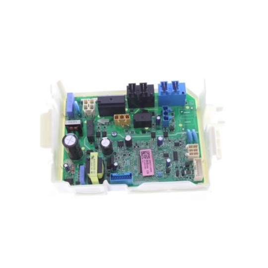
LG EBR85130516 Dryer PCB Main Control Board (PCB Assembly) | HnKParts
#EBR85130516#LGE#Dryer#PCB#MainControlBoard#HnKParts#HomeAppliance#KitchenAppliance#Manufacturer Name:LGE#Product Number:EBR85130516#OEM Part Number:EBR85130516#Order LG EBR85130516 Dryer PCB Main Control Board today! Shop home & kitchen appliance parts at HnK Parts with same-day shipping#available at the best prices.
0 notes
Last Seen Blogs

stars-of-interpol-blog
Starbound's Dumbest Secret Organization

chanchalpro
Untitled

apfezn-blog
APFEZN

fellforher-blog
Sad Post

artdesign4lifeu
artdesgin4life