#PCB materials
Explore tagged Tumblr posts
Visit Tumblr Blog
Explore Tumblr blogs with no restrictions, modern design and the best experience.
Last Seen Tumblr Blogs


Fun Fact
In February 2021, Tumblr had 518.6 million blog accounts.
Text
Cost-Effective Strategies for Efficient PCB Production by A-Gas Electronic Materials
Learn how to optimise PCB production with cost-effective strategies, including design for manufacturability, efficient production techniques, and energy efficiency. Improve quality and reduce costs. Contact A-Gas Electronic Materials for expert guidance and tailored solutions.
#PCB production#cost-effective PCB manufacturing#design for manufacturability#PCB materials#efficient PCB production#supplier collaboration#PCB inventory management#PCB energy efficiency#automated assembly#A-Gas Electronic Materials#UK#PCB production strategies#PCB quality improvement
0 notes
Text
Delve into the world of PCB classification with this comprehensive guide. Viasion explains the different types of PCBs, the materials used in their construction, and their various applications, helping you understand how to select the right PCB for your electronic projects.
0 notes
Text
its so fucked up that im not a hypercompetent mad scientist-engineer that can just build things from scratch constantly. slash genuine.
#if i could take a bunch of spare materials and make my own gadgets i think it would fix me#like down to printing my own pcbs#my ass is not buying a pcb printer#realizing im just my fathers son truly by virtue of him being a junkyard car guy. i need to tear things apart and make new things.#i got that forge of days beast in me#i wish i had a superpower that let me work on really small and precise tech without needing industry grade equipment to guarantee qualtiy#ykwim
6 notes
·
View notes
Text
Important Ohm’s Law Problems for Competitive Exams
A circuit has a resistance of 10 Ω and a current of 2 A. What is the voltage across the circuit?
V= I × R = 2A × 10Ω = 20V
A 24V battery is connected to a resistor of 6 Ω. Find the current flowing through the circuit.

youtube
GET MORE FREE SOLUTION 👈.
#digital learning#online education#online courses#online tutoring#online learning#hesi a2 test#hesi a2 test prep#hesi online classes#electronics manufacturing#electronics industry#electronics components#electronics store#electronics design#vlsi design#electronics#materials#connectivity#computing#ohm's law#flexible circuit board#flex circuit pcb#circuit breaker#electric switch#Youtube
0 notes
Text
Flexible PCB Material for Lightweight and High-Performance Circuits
Our flexible PCB material is engineered for high-performance and durable electronic applications. With superior flexibility, thermal resistance, and excellent conductivity, our flexible PCB material is perfect for wearable devices, medical electronics, and automotive systems.
0 notes
Text
🔧 Unlock the Power of FR-4 Epoxy Fiberglass Sheets! 🔧
Discover how FR-4 epoxy fiberglass sheets are revolutionizing industries with their exceptional electrical insulation and mechanical strength. From PCBs to industrial machinery, these materials are the backbone of modern engineering.
Explore our comprehensive guide to understand their applications and benefits.
#fr43#fr4#fiberglass#epoxy resin#engineering#pcb#industrial design#customsolutions#technology#innovation#manufacturing#materials#electronics
0 notes
Text
ASC’s Expertise in Metal Core Printed Circuit Boards
At American Standard Circuits (ASC), we specialize in crafting exceptional RF metal core printed circuit boards (PCBs) using premium materials. Our metal core PCBs utilize commercially available pre-bonded and post-bonded options for single, double, and multi-layer boards. Post-bonding employs advanced sheet film adhesives, including ASC’s patented adhesives or sweat solder, delivering superior performance.
0 notes
Text
PCB Solder Pallet Materials China: The Ultimate Guide
PCB solder pallet materials are critical components in the electronics production process. These materials are used to form a protective barrier between the PCB and the soldering process, ensuring that the solder only adheres to the intended regions. Manufacturers may obtain consistent and dependable soldering outcomes by employing high-quality Pcb Solder Pallet Materials China, which eventually leads to increased product quality and performance.
View Source: https://medium.com/@jatmaterial159/pcb-solder-pallet-materials-china-the-ultimate-guide-ce4c742fe591

0 notes
Text
PCB Manufacturing Process: All You Need to Know
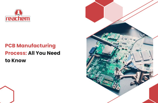
Creating a printed circuit board (PCB) is a systematic process that begins with meticulous design and material selection, crucial for ensuring functionality and durability. The initial steps involve the application of a thin layer of copper over a substrate material, typically a fiberglass substrate reinforced with epoxy resin and glass fiber, which provides the necessary rigidity and electrical insulation. This copper layer is then patterned to form conductive areas that will eventually carry electrical signals.
The layout design process utilizes advanced CAD software for precision, ensuring that the conductive paths and component placement areas are accurately defined. Once the design is finalized, it's transferred onto the PCB using photo reactive chemicals and UV exposure, a process known as outer layer imaging. This method allows for the precise alignment of layers and the creation of intricate circuit patterns.
After the design transfer, the excess copper is removed through a careful etching process, leaving behind the copper traces that form the circuitry. The PCB then undergoes a laminating process to apply a solder mask, a protective layer that covers the entire board while exposing the areas where components will be soldered. This solder mask application is crucial for preventing short circuits and ensuring the longevity of the PCB.
Following the application of the solder mask, a silkscreen printing process adds labels and markings to the PCB, aiding in component placement and board identification. The final step in the fabrication processes involves applying a surface finish, such as tin plating, to protect the exposed copper and ensure a reliable soldering surface. Other surface finishes like HASL (Hot Air Solder Leveling) or ENIG (Electroless Nickel Immersion Gold) are also used depending on the application requirements.
Throughout the PCB manufacturing process, precision is maintained through the use of technologies like CNC machines for accurate drilling of holes that will accommodate electronic components. Each part of the PCB fabrication process, from the initial design to the final surface finish, is critical to enhancing the PCB's electrical performance and longevity.
The final stages of assembly involve the placement of components onto the PCB, often by a contract manufacturer specializing in PCB assembly. This is followed by soldering, which can be done through various methods, to securely attach the components to the board.
Rigorous electrical tests are conducted to validate the PCB's performance, ensuring that it meets stringent quality standards before integration into electronic devices. These tests verify the integrity of the conductive paths, the correct orientation of components, and the overall functionality of the PCB.
This holistic approach underscores the importance of meticulous craftsmanship and thorough quality assurance in producing reliable PCBs that power our modern gadgets effectively. Each step, from the initial plating process to the final surface finishing, contributes to enhancing the PCB's electrical performance and longevity, making it a vital component in the electronics industry.
To read more please visit:
Reachemical chemicals
16479857177
600 Matheson Blvd W Unit 5, Mississauga, Ontario ,ON L5R 4C1.
#thin layer of copper#plating process#excess copper#laminating process#tin plating#fabrication processes#substrate material#exposed copper#solder mask application#circuit board manufacturing process#conductive areas#surface finish#layer alignment#outer layer imaging#parts of the pcb fabrication process#epoxy resin and glass fiber#contract manufacturer#outer layers#electrical tests#photo reactive chemicals
0 notes
Text
PCB Materials Market - Forecast(2024 - 2030)
PCB Materials Market is forecast to reach US$18.3 billion by 2030, after growing at a CAGR of 5.3% during the forecast period 2024-2030. The PCB Materials play a major role in the manufacturing of the PCB (Printed Circuit Boards) since the performance of the PCB primarily depends on the materials used to produce it.
0 notes
Text
Solder Mask vs PCB Solder Resist: Understanding the Differences
Understand the role of solder mask vs solder resist in PCB production. Learn how these coatings enhance electrical insulation, prevent solder bridging, and support UK manufacturing standards. Visit our site for advanced solder mask solutions tailored to your needs.
#solder mask#solder resist#PCB solder mask#PCB solder resist#LPI solder mask#solder mask vs solder resist#PCB surface protection#epoxy solder mask#dry film solder resist#UK PCB manufacturing#high-reliability A-Gas Electronic Materials#circuit board protective coatings
0 notes
Text

Explore commonly used rigid PCBs and their materials. Learn about their applications and benefits, and how Viasion ensures quality in rigid PCB manufacturing.
0 notes
Text
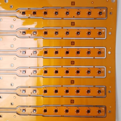
Unraveling the World of Flex Circuit Prototypes: Choosing the Right FPC Manufacturer
Introduction
Flex Printed Circuit Boards (Flex PCBs), often referred to as Flex Circuits, have become indispensable in today's electronics industry. These bendable and versatile circuit boards are a crucial component in various applications, from medical devices and aerospace systems to consumer electronics. When it comes to designing and producing Flex PCB prototypes, choosing the right FPC manufacturer is paramount. In this blog post, we will explore the world of Flex Circuit Prototypes and discuss the key considerations when selecting an FPC manufacturer.
Understanding Flex Circuit Prototypes
Flex Circuit Prototypes are specialized printed circuit boards designed to be flexible, allowing them to conform to intricate shapes or fit into compact spaces. These boards are typically made from flexible substrates like polyimide (PI) or polyester (PET) and can have single or multiple layers, depending on the complexity of the circuit. Flex circuits can be found in products ranging from smartphones and wearable devices to automotive control systems.
Why Choose Flex Circuit Prototypes?
Space Efficiency: Flex PCBs are ideal for applications with space constraints, as they can be folded or bent to fit into tight spaces, reducing the overall size of the device.
Reliability: Flex circuits offer excellent reliability due to their reduced number of interconnects, which minimizes the risk of connection failures and short circuits.
Weight Reduction: Flex circuits are lightweight, making them a preferred choice in applications where weight reduction is critical, such as aerospace and automotive industries.
Durability: These circuits are more robust and can withstand vibrations and shock, making them suitable for applications that experience harsh environments.
Click here for more information: https://www.tumblr.com/fpcway/731599943480000512/exploring-fpc-assembly-flex-pcb-material-and
#Flex PCB#Flex Circuit Prototype#FPC Manufacturer#Flex PCB Material#FPC Prototype#Flexible Printed Circuit
0 notes
Text

Revive Your PCB With Cutting Edge Trace Repair Material
Do you need PCB trace repair material? Visit BEST provides customers with the resources they need for efficient and effective repairs and modifications of lands, contact fingers, traces, and SMT pads through a selection of PCB repair kits and materials. For additional information, go to http://www.soldertools.net/pcb-repair-kit-1.
0 notes
Text
"As the world grows “smarter” through the adoption of smartphones, smart fridges, and entire smart houses, the carbon cost of that technology grows, too.
In the last decade, electronic waste has become one of the fastest-growing waste streams in the world.
According to The World Counts, the globe generates about 50 million tons of e-waste every year. That’s the equivalent of 1,000 laptops being trashed every second.
After they’re shipped off to landfills and incinerated, the trash releases toxic chemicals including lead, cadmium, arsenic, mercury, and so much more, which can cause disastrous health effects on the populations that live near those trash sites.
Fortunately, Franziska Kerber — a university student at FH Joanneum in Graz, Austria — has dreamed up a solution that helps carve away at that behemoth problem: electronics made out of recyclable, dissolvable paper.
On September 11, Kerber’s invention “Pape” — or Paper Electronics — earned global recognition when it was named a national winner of the 2024 James Dyson Awards.

When she entered the scientific competition, Kerber demonstrated her invention with the creation of several small electronics made out of paper materials, including a fully-functional WiFi router and smoke detector.
“Small electronic devices are especially prone to ending up in household waste due to unclear disposal systems and their small size, so there is significant potential to develop a more user-friendly end-of-life system,” Kerber wrote on the James Dyson Award website.
“With this in mind, I aimed to move beyond a simple recycling solution to a circular one, ensuring long-term sustainability.”
Kerber’s invention hinges on crafting a dissolvable and recyclable PCB board out of compressed “paper pulp.”
A printed circuit board (PCB) is a board that can be found in nearly all modern electronic devices, like phones, tablets, and smartwatches.
But even companies that have started incorporating a “dissolution” step into the end life of their products require deconstruction to break down and recover the PCB board before it can be recycled.
With Kerber’s PAPE products, users don’t need to take the device apart to recycle it.
“By implementing a user-friendly return option, manufacturers can efficiently dissolve all returned items, potentially reusing electronic components,” Kerber explained.
“Rapidly advancing technology, which forms the core of many devices, becomes obsolete much faster than the structural elements, which are often made from plastics that can last thousands of years,” Kerber poses.
PAPE, Kerber says, has a “designed end-of-life system” which anticipates obsolescence.
“Does anyone want to use a thousand-year-old computer?” Kerber asks. “Of course not. … This ensures a sustainable and reliable system without hindering technological advancement.”"
-via GoodGoodGood, September 13, 2024
#ewaste#e waste#e waste recycling#e waste management#e waste solutions#paper#sustainability#green tech#tech news#sustainable technology#recycling#good news#hope
586 notes
·
View notes
Text
Writing Scientist Characters
this post is mainly an excuse to post a certain list of lab supplies I've made for a friend and infodump about lab work. but feel free to use this as a little resource when writing characters who are scientists and/or lab nerds. who knows, maybe it'll be of use.
General thoughts
Many people think it's a stereotype that scientist or nerd characters talk using complex technical jargon. While that is true to an extent, there actually is some kind of lab jargon. It varies across different labs and fields, but one thing they have in common is that it seeks to simplify, not the other way around.
gelelectrophoresis becomes elpho
microbiology becomes mibi
deioninized water becomes aqua dist
biochemistry becomes BC
sodium hydroxide becomes NaOH
They will probably not call a glass of water "silicon dioxide and h2o".
...and more. feel free to get creative. If you're writing in any other language than English, you can throw in one or two anglicisms as well. Also, most scientists will never gatekeep their work, and in an opposite fashion, will not shut up about it unless you make them. And no, most chemists do not know the entire periodic table by heart, only the most relevant elements. (main groups and a few commonly used metals of the subgroups) When it comes to characters doing the lab work, keep in mind that there are a lot more people involved than the scientist themself. Most scientists are more occupied with paperwork and data analysis, it is the laboratory technicians and assistants that do most of the practical work. They often have more lab experience than the scientists themselves.
Things you can have your lab nerd character do instead of making random chemicals explode
writing a lab report (and losing their mind over excel)
degreasing the glass bevel stoppers
removing the permanent marker from beakers (labeling is important)
complaining about the lack of funding of [their field] research
cleaning glassware
preparing specimen for examination
googling the most basic equations for their report
checking if the glassware and utensil collections are complete
steal single use plastic pipettes from their lab
pirating expensive textbooks
A list of laboratory supplies and utensils you can have them work with
Laboratory general (chem + bio)
Erlenmayer flasks, beakers, precision scales (3 digits), glass rods, metal spoons/spatulas, screw on glass flasks (autoclave compatible) test tubes, stopcock grease, dispensers with sanitizer and hand cream, gas burners, heating plates, eppendorf pipettes, pipette tips, Peleus pipetting aids, squirting bottles, liquid and powder funnels, incubator/drying chamber, round watch glasses, magnet stirring plates.
Microbiology Autoclave, petri dishes, agar plates, innoculation loops (reusable and metal), clean bench, microscope slides, microscope, drigalski-spatula, test tubes with clamping lids
Histology
Paraffin bath, water bath, scalpels, scissors, razor blades, microtomes (rotating microtome, slide microtome and freezing microtome), histocinette, tweezers (various kinds), ocular
Biochemistry
Sequencing robots, eppendorf tubes, gelelectrophoresis chambers, centrifuge
Analytical Chemistry
Photometer, kuvettes, burettes, mass spectro meters, UV bank (for chromatogrophies), pyknometers, melting point meter, porcelain mortars, pH paper, analytical scales (4 or more digits)
Prep Chemistry
Tripod/standing material, miniature lifting platforms, spiral condenser, colon condenser, round bottom flask (three necked and y- necked), filtration material, Separating funnel
Electrical engineering
Electric generators, Soldering iron, Clamp connectors, plugin connectors, ohm’s resistors, plug in lamps, condensers, transistors, PCBs, amperemeters, voltmeters, multimeters
Mechanics
Tripod/standing material, metal hooks, metal rods, mechanical stop watches, marbles, metal springs, Newton meters, laser motion detectors
Optics
Prisma (various kinds), various glass lenses (concave, convex, biconcave, biconvex), laser pointers, optical bench, mechanical iris diaphragm, looking glasses, monochrome lamps, lamp filters
Most used chemicals
Deionized water, ethanol, NaOH, HCl, H3PO4, NaCl (+ physiological NaCl solution 0.9)
Useful websites for writing science stuff
DNA sequence generator (simple): http://www.faculty.ucr.edu/~mmaduro/random.htm
DNA, RNA and protein sequence generator: https://molbiotools.com/randomsequencegenerator.php Annealing temperature calculator: https://tmcalculator.neb.com/#!/main
Medicine name generator: https://www.fantasynamegenerators.com/medicine-names.php Anything chemistry related: https://www.wolframalpha.com/input?i=chemistry
Commonly used software:
MS Excel
Yenka
CASSY Lab
LabView
SpectraLab
LIMS
LaTex
Slack
Scientist friends, feel free to add onto this.
Have fun writing!
#creative writing#writing#resource#writing resources#science#biology#chemistry#physics#writing guide#writers on tumblr#writeblr#rp#rp resources
116 notes
·
View notes