#PTH PCB
Explore tagged Tumblr posts
Visit Tumblr Blog
Explore Tumblr blogs with no restrictions, modern design and the best experience.
Last Seen Tumblr Blogs


Fun Fact
Tumblr is available in 18 languages.
Text
What is PCB Assembly ?
PCB Assembly manufacturer - Hitech Circuits Co., Limited
It’s the step in the manufacturing process in which you populate a blank board with the electronic components needed to make it into a functional printed circuit board. It’s these components that make a board into the circuit that enables an electronic product to function. PCB assembly typically takes place via one of two processes:
1. Surface-mount technology
SMT: SMT stands for “Surface Mount Technology“. The SMT components are very small sizes and comes in various packages like 0201, 0402, 0603, 1608 packages for resistors and capacitors. Similarly for Integrated circuits ICs we have SOIC, TSSOP, QFP and BGA.
The SMT components assembly is very difficult for human hands and can be time taking process so it is mostly done by automated pick and place machine.
2. Through-hole manufacturing
THT: THT stands for “Through hole Technology”. The components with leads and wires, like resistors, capacitors, inductors, PDIP ICs, transformers, transistors, IGBTs, MOSFETS are example.
The component has to be inserted on one side of PCB and pulled by leg on other side and cut the leg and solder it. The THT components assembly is usually done by hand soldering and is relatively easy.
Printed Circuit Board Assembly Techniques
There are only two common PCBA techniques available for use by a PCB designer. The methods are:
1. Automated PCB Assembly Techniques
Generally, this technique employs the use of state of the art machines, which are fully automatic. For example, the surface mount components are worth positioning with the aid of an automated pick and place machine.
Again, reflow soldering is commonly for surface mount components usually done in a reflow oven. An automated solder stencil is also used to apply the solder paste on the PCB.
Finally, high tech inspection machines are used to confirm and check the quality of the PCBA. Some of which include: Automated optical inspection machine (AOI), X-ray inspection machines, etc.
Above all, due to the precise monitoring, control of soldering, no human input and versatile machines.
This technique ensures utmost efficiency, output consistencies, and limits defects.
2. Manual PCB Assembly Techniques
This method is favorite for use with through-hole parts, which needs manual placement on the board. Besides, with these through-hole parts, it’s advisable you use wave soldering. Note that in the through- hole assembly process, you need to place the components and electronics on the PCB.
After that, you use wave soldering to solder the leads. Typically, you will need an individual to insert a component into a marked PTH. Once done, transfer the PCB to the next station where the next person will be on standby tasked with fixing another part.
What are the Benefits of SMT PCB Assembly?
SMT assembly provides many benefits and some of them are as follows:
It can be used to incorporate small components.
In SMT, the components can be placed on both sides of the board.
It assures high component densities.
Fewer holes need to be drilled for surface mounting than through-hole.
It require low initial costs and time for setting up the mass production.
SMT is the simpler and faster-automated assembly when compared to through-hole.
Errors regarding the component placement can be easily rectified.
Surface mount PCBs feature strong joints, which can easily withstand vibrations.
What are the techniques used in Surface Mount Technology?
There are several techniques for the reflow process. After applying the solder paste or a flux mixture on the board and after placing the components, the boards are conveyed to a reflow soldering oven. The techniques used for reflowing soldering include infrared lamps, hot gas convection, fluorocarbon liquids with a high boiling point, and so on.
What are the different testing methods used in SMT PCB Assembly?
Hitech Circuits as the PCB assembly manufacturer, we perform the following testing and inspection to ensure the quality of surface mount PCBs.
Automated Optical Inspection (AOI): This is performed before and after the soldering to identify the component placement, presence, and solder quality.
X-ray Testing: In this type of testing, the operator relies on the X-ray images of the PCB to check the solder joints and lead-less components such as Quad Flat Packs and ball grid arrays, which are generally not visible to naked eyes.
In-Circuit Testing (ICT): This method is used to detect manufacturing defects by testing the electrical properties in the SMT Assembly.
What type of files or documents should I send for SMT PCB Assembly?
Gerber Files: The file contains all details of physical board layers including solder masks, copper layers, drill data, legends, and so on.
Bill of Materials (BOM): This contains information on the list of items needed for the PCB manufacturing and the instructions of manufacturing.
Pick and Place File: This file contains information on all components to be used in the PCB design and their rotation and X-Y coordinates.
The whole process of PCB Assembly
1. Bare board loader machine
The first step in the PCB assembly is to arrange the bare boards on the rack, and the machine will automatically send the boards one by one into the SMT assembly line.
2. Printing solder paste
When PCB on the SMT production line, firstly, we have to print solder paste on it, and the solder paste will be printed on the pads of the PCB. These solder pastes will be melt and solder the electronic parts to the circuit board when it passes through the high-temperature reflow oven.
In addition, when testing new products, some people will use film board/adhesive cardboard instead of solder paste, which can increase the efficiency for adjusting the SMT machines.
3. Solder paste inspection machine(SPI)
Since the quality of solder paste printing is related to the quality of welding of subsequent parts, some SMT factories will use optical machine to check the quality of solder paste after printed the solder paste in order to ensure stable quality. If there any poorly printed solder paste board, we will wash off the solder paste on it and reprint, or remove the excess solder paste if there is redundant solder paste on it.
4. High speed SMT machine
Usually, we will put some small electronic parts (such as small resistors, capacitors, and inductors) to be printed on the circuit board first, and these parts will be slightly stuck by the solder paste just printed on the circuit board, so even if the speed of printing is very fast and the parts on the board will not fall away. But large parts are not suitable for use in such high speed SMT machines, which will slow down the speed of small parts assembly. And the parts will be shifted from the original position due to the rapid movement of the board.
5. Universal SMT machine
Universal SMT machine is also known as "slow machine", it will be assembled some large electronic components, such as BGA IC, connectors, etc., these parts need more accurate positions, so the alignment is very important. Use a camera to take a picture to confirm the position of the parts, so the speed is much slower than High speed SMT machine we taked before. Due to the size of the components here, not all of them are packed in tape and reel, and some may be packed in trays or tubes. But if you want the SMT machine to recognize the trays or tube-shaped packaging materials, you must configure an additional machine.
Generally, traditional SMT machines are using the principle of suction to move electronic parts, and in order to place the parts successfully, and there must be the flat surface on these electronic components for the suction nozzle of the SMT machine to absorb. However, for some electronic parts don’t have a flat surface for these machines, and it is necessary to order special nozzles for these special-shaped parts, or add a flat tape on the parts, or wear a flat cap for thees electronic parts.
6. Manual parts or visual inspection
After assembled all parts by the high speed SMT machine or Universal SMT machine and before going through the high-temperature reflow oven, and we will set up a visual inspection station here and to pick out the deviation parts or missing components boards etc., because we have to use a soldering iron to repair if there are still defectives boards after passing the high-temperature oven, which will affect the quality of the product and will also increase the cost. in addition, for some larger electronic parts or traditional DIP parts or some special reasons cannot be processed by the SMT machine before, they will be manually placed on pcb here.
7. Reflow oven
The purpose of reflow oven is to melt the solder paste and form a non-metallic compound on the component feet and the circuit board, that means to solder electronic components on the circuit board. The temperature rise and fall curves often affect the soldering quality of the entire circuit board. According to the characteristics of the solder materials, usually the reflow oven will set the preheating zone, soaking zone, reflow zone, and cooling zone to achieve the best soldering effect.
For example, the melting point for SAC305 solder paste with lead-free is about 217°C, which means that the temperature of the reflow oven must be higher than the melting points to remelt the solder paste. What's more, the maximum temperature in the reflow furnace should not exceed 250°C, otherwise many parts will be deformed or melted because they cannot withstand such a high temperature.
Basically, after the pcb passed through the reflow oven, the assembly for the entire circuit board is almost complete. If there are hand-soldered parts, we need to transfer to DIP process, and then we have to check the quality after reflow oven by QC department.
8. Automatic optical inspection(AOI)
The main purpose of setting up AOI is because some high density boards can’t be process the following ICT test, so we used AOI inspection to replace it. But even using AOI inspections, there still have the blind spots for such checking, for example, the solder pads under the components cannot be checked by AOI. At present, it can only check whether the parts have side standing issue, missing parts, displacement, polarity direction, solder bridges, lack of soldering etc., but cannot checking the BGA solderability, resistance value, capacitance value, inductance value and other components quality, so far AOI inspection can’t completely replace ICT test.
Therefore, there is still some risk if only AOI inspection is used to replace ICT testing, but ICT test is also not 100% make sure the good quality, we suggest these two ways can be combined with together to make sure the good quality.
9. PCB unloader machine
After the board is fully assembled, it will be retracted to the unloder machine, which has been designed to allow the SMT machine to automatically pick and place the board without damaging the quality for PCB.
10. Visual inspection for finished products
Normally there will be a visual inspection area in our SMT production line whether there is an AOI station or not, and it will help to check if there are any defectives after completed assembled the pcbs. If there is an AOI station, it can reduce the visual inspection worker on our SMT line, and to reduce the potential cost, and because it is still necessary to check some places that cannot be judged by AOI, many SMT factories will provide the mainly visual inspection templates at this station, which is convenient for visual inspection worker to inspect some key parts and polarity for components.
11. DIP process
DIP process is a very important process in the whole PCBA processing, and the processing quality will directly affect the functional for PCBA boards, so it is necessary to pay more attention to the DIP process. There are many preliminary preparations for DIP process. The basic process is to re-process the electronic components first, like to cut the extra pins for some DIP components, our staff received the components according to the BOM list, and will check whether the material part numbers and specifications are correct or not, and performs pre-production pre-processing according to the PCBA samples. The steps are: Use various related equipment (automatic capacitor pins cutting machine, jumper bending machine, diode and triode automatic forming machine, automatic belt forming machine and other machines) for processing.

12. ICT test
Printed Circuit board open/short circuit test (ICT, In-Circuit Test), The purpose of ICT test is mainly to test whether the components and circuits on the printed circuit board are open or short issues. It can also measure the basic characteristics of most components, such as resistance, capacitance, and inductance values to judge whether the functions of these parts are damaged, wrong parts or missing parts etc. after passing through the high-temperature reflow oven.
ICT test machines are divided into advanced and basic machines. The basic ICT test machines are generally called MDA (Manufacturing Defect Analyzer). It’s just to measure the basic characteristics of electronic components and judge open and short circuits issue we talked above.
In addition to all the functions of the basic ICT test machines, for advanced ICT test machine can also test the whole PCBA by using power, start to testing the PCBA boards by setting the program in the test machine. The advantage is that it can simulate the function of the printed circuit board under the actual power-on condition, this test can partly replace the following functional test machine (Function Test). But the cost for the test fixture of this advanced ICT test can probably buy a car, it’s too expensive and we suggest it can be used in mass production products.
13. PCBA function test
Functional testing is to make up for the ICT test, because ICT only tests the open and short circuits on the the PCBA board, and other functions such as BGA and other fuctions are not tested, so it is necessary to use a functional testing machine to test all functions on the whole PCBA board.
14. Cutting board (assembly board de-panel)
Normally, printed circuit boards will be produced in panel, and it will be assembled to increase the efficiency of SMT production. It means several single boards in one panel, such as two-in-one, four-in-one etc. After finished all the pcb assembly process, it needs to be cut into single boards, and for some printed circuit boards with only single boards also need to cut off some redundant board edges.
There are several ways to cut the printed circuit board. You can design the V-cut using the blade cutting machine (Scoring) or directly manually break off the board (not recommended). For more high density circuit boards, it will be used the professional splitting machine or the router to split the board without any damage the electronic components and printed circuit boards, but the cost and working hours will be a little longer.
Why Choose Hitech Circuits PCB Assembly Manufacturer for Your PCB Assembly Projects?
There are several PCB manufacturers specializing in PCB assemblyservices. However, Hitech Circuits PCB Assembly stands out owing to the following:
Assistance in Material Procurement:
Technically, in PCB assembly services, the quality of parts is the responsibility of the OEM; however, we ease your job by assisting you to make the right selection. We can help you procure all your parts of the same type own a single part number, thanks to our supply chain and vendor network as well as experience. This saves time and cost that goes in ordering single parts as you plan.
Testing procedures:
We are very focused on quality and thus implement stringent testing procedures at each stage of the assembly and after completion.
Fast Turnaround Times:
Our well-equipped facility and the right tools enable us to complete your requirements well before time, and without compromising on the quality or functioning of the PCBs. For simple designs we revert in 24 to 48 hours.
Cost Effectiveness:
While PCB assembly is a cost-effective alternative, we go a step further and assure that the parts you list are of a good quality and suitable for your requirement. Also, you can control the part flow and replenish them as needed. This eliminates the need to buy extra stock and store it.
Quick Quote:
We offer a quick quote based on your BOM. All you need is a detailed BOM, Gerber files, your application requirement sheet, and quantity.
We’re not one to stand still, which is why we use the latest equipment and the finest minds to create your PCB projects. We’re constantly keeping our finger on the pulse of the latest trends. And as a result, we know how to deliver the highest standards of PCB assembly to meet all your requirements.
Our dedicated, friendly customer service team also means that we support you every step of the way. Offering our expert guidance to ensure a complete PCB project that you’re happy with.
Contact us today
No matter what your printed circuit board assemblyneeds are, we always aim to deliver efficient, dependable solutions. For more information about our services, do not hesitate to get in touch with us today for a no-obligation quote
2 notes
·
View notes
Text
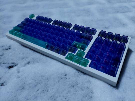
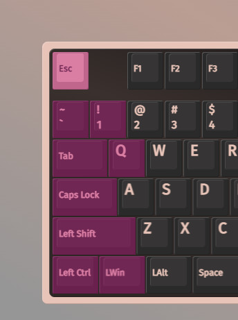
Leopold FC980m
Custom PCB (source)
Aflion Melody and Runner switches
Deadline Studio AirR PC keycaps
Lightblue painted stock aluminium plate
Stock plate-mounted clip-in stabilizers
More under the cut.

This build took well over a year to actually get it to it's current state and it's technically not done yet, considering I still have to tune and lube the stock stabilizers.
Issue number 1 before everything else was getting the cherry mx brown switches out of the old PCB to be able to remove the plate because I didn't want to order a custom plate or go plateless. The solder used on the original PCB has a stupid melting point so not only did I have to dilute the solder with my own that melts at roughly 320°c, but my soldering iron was set to 410°c (or more for specific spots, more on that later). A good chunk of the extracted switches were simply not usable anymore afterwards from being slightly molten. The plate has a few hooks and the PCB has holes for them to hook into, one of which is a PTH (plated through hole) hole that goes to the PCB's ground and the corresponding hook lacks paint and is soldered into this hole. This cursed and damned hook was the reason for a lot of frustration as it took quite literally half an hour (maybe more) to de-solder at 435°c while constantly adding and removing solder to slowly chip away at this literal mountain of solder they used.
My next problem was simply getting the new PCB(s). Back then I was a bit tight on money from expenses out of my other hobbies and various mundane things I needed, so it took a month or two to be able to finally order them. Except JLCPCB, the service that was recommended for this PCB by this keebtalk thread, ran out of the MCUs I needed, so I researched if they had any alternatives, but by the time I read enough of the documentation of various alternatives and found one, that one ended up being out of stock as well. So another couple of months passed basically just waiting.
After ordering, an engineer of JLCPCB contacted me because some of the NPTH (non-plated through hole) holes were too close to each other and would be at risk of breaking while drilling and the best option seemed to be just making them PTH holes, because the hook holes aren't connected to anything and the plate's paint makes it non-conductive anyways so it should be fine. Right?
FORESHADOWING IS A LITERARY DEVI-
I eventually get the new PCBs and of course immediately scratch one of the 5 I ordered (it still works), tested 2 of them and went to work. Across a couple months (I was preoccupied, blah blah lazy excuses) I slowly chipped away at soldering in the MillMax sockets.
Couldn't have 4 minutes without problems though, now can we? Trying to install the switches and PCB didn't work because the MillMax sockets add roughly a millimeter of distance between PCB and plate and you can already guess that this doesn't play nice with the plate's hooks. I trimmed off the hooks but left them as little poles for aligning the PCB and so everything would be alright. Right?

I assemble the keyboard fully and plug it in to see... it not working. I assumed due to the extra millimeter from the hotswap sockets messing with the tolerances, there may be a short to the daughter board, so I took it apart again and taped any contacts and it still didn't work after reassembly. Now I was getting quite annoyed so I took off the top of the casing and tested it like that and surprisingly it worked. Kinda.
As soon as I snapped the top of the case back on, or pressed down on the plate in the bottom left corner, the keyboard would fire A bunch of keys at the same time.
Seeing this set of keys led me to the right path. I double checked this side of the PCB and saw that the hole for the PCB hook next to caps was PTH rather than NPTH and connected to one of the contacts for caps. Remember when I said one of the hooks was connected straight to ground? Or how I had to remove part of the plate hooks, thus removing the paint that prevents it from conducting electricity? Yeah. One strip of tape later and everything is fixed and works perfectly fine.
That's basically it. It was a pain, but it looks, sounds and types nicely. I'm happy with how it turned out.
2 notes
·
View notes
Text
Absolute EMS and the Evolution of Next-Gen PCB Assembly Services
The assembly of electronics is a vast, evolving field, filled with challenges. Automation has sparked a quiet revolution in the industry, and it continues to shift in that direction. Within this constantly changing horizon of electronics assembly - precision, reliability, and efficiency drive advancement. Absolute EMS, a leader in PCB Assembly Services (PCBA or EMS), offers cutting-edge assembly solutions to demanding high-performance OEMSs. Their technological expertise in press-fit connectors in silicon valley guarantees a strong interconnect without the inconveniences inherent in conventional soldering.

The Engineering Behind Press-Fit Connectors
Press-fit connectors are a replacement for conventional soldered connections, providing a very reliable mechanical and electrical interface. The connector pins have compliant sections that form a gas-tight joint when pressed into plated through-holes (PTHs) of a PCB. The process provides:
Uniform Contact Pressure: Uniform pressure inside the hole is delivered through elastic deformation of the flexible pin, keeping the micro-movements low and signal attenuation low.
Elimination of Soldering Defects: Defects such as cold joints, solder bridges, and thermal stress are fully eliminated.
Superior Mechanical Retention: High insertion pressure and frictional locking avoid removal by shock and vibration.
Improved High-Frequency Signal Integrity: The uniform contact resistance minimizes electromagnetic interference (EMI) and ensures reliable data transmission in RF and high-speed digital circuits.
Complementary High-Precision PCB Assembly Techniques
Absolute EMS also integrates other cutting-edge methodologies in PCB assembly, ensuring adherence to stringent industry standards such as IPC Class 3 for high-reliability applications. These capabilities include:
High-Density Surface Mount Technology (SMT): Advanced pick-and-place systems handle micro-BGAs, fine-pitch QFNs, and 01005 components for compact, high-performance designs. And large BGA (4k+ balls) pick and place.
Selective Through-Hole Technology (THT): Precision-controlled soldering techniques, including wave soldering and selective soldering, enhance the integrity of mechanical and power connections without disturbing other components on the board..
Hybrid Assembly Solutions: A combination of SMT and PTH and that enables complex multi-layer PCB configurations suited for demanding applications.
Automated Optical Inspection (AOI)and X-Ray Inspection: Ensuring defect-free assembly through real-time analysis and verification of solder joints, component placement, and internal structure.
Final Thoughts
For companies looking for Electronic Manufacturing Services , Absolute EMS provides specialized solutions in press-fit connectors, based in Silicon Valley. They constantly strive to deliver the best technology and their dedication to quality, efficiency, and technology makes them a go-to partner for all the high tech OEMS in Silicon Valley and beyond.
To see their entire range of PCB assembly services, contact Absolute EMS and learn how they can get your product to market faster with their electronic manufacturing processes.
0 notes
Text
Studiomaster PA Series: The Benchmark in Professional Amplifiers
When it comes to professional audio amplification, the Studiomaster PA series stands out as a powerhouse lineup designed for exceptional performance, durability, and reliability. Each model within this series delivers cutting-edge technology combined with meticulous engineering to meet the demands of audio professionals. Let's dive into the details of each model in the PA series, ranging from the compact PA 1.5 to the flagship PA 10.0.
Studiomaster PA 1.5: Compact yet Powerful
The PA 1.5 is the ideal choice for setups requiring high-quality sound and efficient performance in a compact form. With its combination of switch mode and linear power supplies, the PA 1.5 ensures smooth operation even in environments with fluctuating voltage levels as low as 130V. a

Key Features:
Input Options: Balanced XLR and 1/4” Stereo Jack.
Modes: Stereo, Mono, and Bridge for versatile application.
Cooling: Intelligent low-noise variable-speed fans with efficient heatsinks.
Transformers: High-current toroidal transformers with high-grade cores for greater transient response and low noise, even at 2 Ohms.
Indicators: Mute, Signal, Clip, and Fault LEDs for performance monitoring.
Operational Efficiency: Rated for 2Ω operation with a sensitivity switch (+4 dB or 0 dB).
Additional Protection: Low-cut and Limiter switches for optimal speaker performance.
PCB Design: High-quality glass epoxy, double-sided PTH PCBs, and high-grade components ensure reliability even in tough ambient environments.

Slightly more powerful than the PA 1.5, the PA 2.0 delivers enhanced audio performance while retaining the reliability and flexibility synonymous with the PA series.
Key Features:
Durable Construction: High-quality glass epoxy, double-sided PTH PCBs with high-grade components ensure reliability even in tough ambient environments.
Versatile Input: Supports both Balanced XLR and 1/4” Stereo Jack.
Flexible Modes: Stereo, Mono, and Bridge modes for varied setups.
Cooling Mechanism: Advanced heat management with noise-controlled fans.
Protection Mechanisms: Switchable Low-cut and Limiter switches.
Performance Monitoring: Comprehensive LED indicators.
Transformers: High-current radial transformers with high-grade cores for low noise and excellent transient response.
Studiomaster PA 3.0: For Medium to Large Venues
The PA 3.0 amplifier is designed for medium to large scale audio setups. It offers superior sound quality and robust power output, making it a popular choice among audio professionals.

Key Features:
High Efficiency: Switch mode and linear power supplies for seamless performance.
Cooling System: Low noise fans and optimized heat sinks for reliability.
Enhanced Inputs: Balanced XLR and 1/4” Stereo Jack.
Operational Modes: Stereo, Mono, and Bridge for various applications.
Durability: Built with high-quality glass epoxy PCBs and premium components.
Protection & Monitoring: Equipped with Low-cut and Limiter switches along with comprehensive LED indicators.
Advanced Transformers: High-current toroidal transformers ensure consistent performance and reduced noise.
Studiomaster PA 4.5: Versatility Meets Power
The PA 4.5 is a step up in terms of power and features, making it a versatile solution for professional audio requirements. It’s built to withstand demanding conditions while delivering exceptional audio clarity.

Key Features:
Robust Design: High-grade components and durable construction ensure longevity.
Cooling Efficiency: Intelligent fans with heat management systems.
Flexible Modes: Operates in Stereo, Mono, and Bridge modes.
Comprehensive Monitoring: Mute, Signal, Clip, and Fault LED indicators.
Protection Features: Low-cut and Limiter switches for speaker safety.
Enhanced Connectivity: Balanced XLR and 1/4” Stereo Jack inputs.
Reliable PCB: Glass epoxy, double-sided PTH PCBs for durability in tough environments.
Studiomaster PA 6.0: Professional Power Amplification
The PA 6.0 delivers professional grade audio performance, making it a reliable choice for larger venues and events. Its advanced cooling and power management features ensure consistent output even under demanding conditions.

The PA 6.0 delivers professional grade audio performance, making it a reliable choice for larger venues and events. Its advanced cooling and power management features ensure consistent output even under demanding conditions.
Key Features:
Power Supply: Combination of switch mode and linear power supplies.
Durability: Built with glass epoxy PCBs and premium grade components.
Connectivity: Balanced XLR and 1/4” Stereo Jack inputs.
Cooling System: Variable speed fans and direct mounted heat sinks.
Operational Flexibility: Stereo, Mono, and Bridge modes.
Additional Features: Low-cut and Limiter switches for optimal performance.
Transformers: High-current toroidal transformers with high-grade cores provide superior transient response and low noise.
Studiomaster PA 7.5: High-End Power Amplifier
The PA 7.5 is designed for professional applications requiring high power and uncompromising audio quality. It’s ideal for concerts, large auditoriums, and high energy events.

Key Features:
High Power Output: Suitable for demanding audio setups.
Advanced Cooling: Low noise fans and efficient heat dissipation.
Operational Versatility: Stereo, Mono, and Bridge modes.
Durable Build: High-quality components and robust construction.
Protection: Includes Low-cut and Limiter switches.
Monitoring Indicators: Comprehensive LED status indicators.
Reliable Transformers: High-current toroidal transformers deliver consistent performance with low noise.
Studiomaster PA 10.0: The Ultimate Powerhouse
As the flagship model, the PA 10.0 represents the pinnacle of Studiomaster’s engineering excellence. It combines high power output with unparalleled sound clarity, making it the go to amplifier for the most demanding professional audio scenarios.

Key Features:
Unmatched Power: Delivers exceptional sound quality at high power levels.
Cooling Technology: Intelligent cooling system with variable speed fans.
Operational Modes: Stereo, Mono, and Bridge modes for diverse applications.
Input & Output: Balanced XLR, 1/4” Stereo Jack, and Speak-on output connectors.
Advanced Monitoring: Mute, Signal, Limiter, and Temperature LED indicators.
Protection Mechanisms: Equipped with Low-cut and Limiter switches for speaker safety.
PCB & Transformers: High-quality glass epoxy PTH PCBs and toroidal transformers ensure reliability and superior performance.
Conclusion : The Studiomaster PA series offers a range of amplifiers catering to every professional audio need. From the compact PA 1.5 for smaller setups to the PA 10.0 for high powered events, each model guarantees exceptional sound quality, operational reliability, and user friendly features. Whether you’re an audio enthusiast or a seasoned professional, the PA series has an amplifier that fits your needs perfectly. Explore the Studiomaster PA series and elevate your audio experience to the next level!
0 notes
Text

Dry Film Lamination:Attach Photosenstive Film
After PTH,PCB will be bonded with dry film by hot press roll.The dry film will be laminated on pretreated boards.
#pcb#flex pcb#rigid-flex pcb#flex circuit pcb#flexible pcb board#flexible circuit board#fpcway#fpcway.com#www.fpcway.com#today on tumblr
0 notes
Text
Luphi Electronics see you at Electronica 2024(Munich,Germany)

Electronica 2024 will cover the entire electronics spectrum, featuring everything from components to systems. Luphi Electronics participates in the 2024 Germany Munich Electronics Fair, from November 12 to 15, 2024. Welcoming numerous professionals from various countries to visit LuphiTouch ( Hall C6, Booth 341.8)!
About Luphi Electronics
Dongguan Luphi Electronics Technology Co., Ltd. (Trademark: LuphiTouch) was established in 2015. The factory covers 4500 square meter. We have 80+ workers and we have been certified by ISO9001, ISO13485, ISO14001 and ISO45001. LuphiTouch mainly focuses on various kinds of human machine interface switch panels, keypads and modules development and manufacturing. Our capabilities cover from mechatronic design, graphic art design, function control PCBA development, MCU development, IC programming, embedded system development to tools making, prototypes making, function testing, mass production and shipping of one-stop total solutions service. We also provide circuit board manufacturing, components sourcing, SMT&PTH assembly, EMS contract manufacturing service for our end clients.

On this fair, Luphi Electronics will show our high quality Products include:
· Medical Membrane Switches(Medizinische Folientasten)
· Backlighting Membrane Switches(Hinterleuchtete Folientasten)
· FPC Membrane Switches(FPC-Folientasten)
· PCB Membrane Switches(PCB-Folientasten)
· Silicone Rubber Keypads(Gummitasten)
· Capacitive Membrane Switches(Kapazitive Folientasten)
· Backpanel Membrane Keypads (Rückseiten-Folientasten)
· Touchscreen & LCDs(Touchscreens und LCDs)
· User Interface Modules(Benutzeroberflächen module)
......
We serve various industries such as medical, industrial control, home appliances, new energy, instrumentation, rail transportation, aviation and navigation, network communications, and mechanical equipment.
Our Commitment to Quality
At Luphi Electronics, we prioritize quality and innovation. Our manufacturing processes are certified under ISO standards (ISO9001, ISO14001, ISO13485, and ISO45001), ensuring that our products meet the highest industry standards. We are proud to be the first ISO13485-certified membrane switch factory in China, we sincerely expect your inquires and look forward to the long-term & stable cooperation with your company!
Professional HMI Switch Sub-assemblies & Touch Display Modules Provider!
Luphi Electronics official website: https://www.luphitouch.com
0 notes
Text
¿¿ qué es una placa de circuito rígida y suave? Como su nombre indica, los PCB flexibles rígidos son una mezcla de PCB flexibles y PCB rígidos. La combinación de estas dos placas aprovecha las ventajas proporcionadas por cada una de ellas para integrar la versatilidad de las placas flexibles con la solidez de las placas rígidas. Las placas de circuito impreso rígidas y flexibles se utilizan en diseños mecánicos más complejos, eliminando los cables flexibles y el cableado y reemplazándolos por circuitos integrados.
Según la definición, el PCB rígido - flexible es una combinación de componentes rígidos conectados interconectando áreas flexibles, en las que el material flexible se utiliza en toda la zona del pcb. Las piezas rígidas se refieren a lugares donde no hay requisitos de flexión. Del mismo modo, el PTH se conecta de una capa a otra según sea necesario. La combinación de rigidez y suavidad también puede adoptar otras tecnologías según sea necesario, como el hdi. A diferencia de los PCB flexibles rentables, los PCB flexibles rígidos pueden ser más costosos debido a su diseño complejo. El diseño de PCB combinado rígido y suave se puede utilizar para eliminar o reducir significativamente los requisitos para arneses de cables voluminosos y caros, reduciendo así los costos y acortando el tiempo de montaje. Al igual que los PCB puramente flexibles, un gran número de PCB rígidos y flexibles se utilizan en aplicaciones aeroespaciales y espaciales, así como en automóviles y equipos de prueba.
0 notes
Text
Understanding Drilling Compensation
1. Why is Drilling Compensation Necessary?
When customers provide PCB files, the hole diameters usually refer to the finished hole size. However, during PCB production, copper plating (or surface treatments like hot tin, gold plating, OSP, or hot tin) occurs inside the holes, causing the diameter to shrink. To ensure that the finished hole size meets requirements, engineering CAM performs drilling compensation to correct the hole size.
Example: If the finished hole size is 1.00 mm with surface treatment (Nickel thickness: 2.54 μm, Gold thickness: 0.0254 μm) and IPC standard class II (average copper thickness: 20 μm), a compensation of 0.10 mm would require the engineering team to select a drill bit of 1.10 mm.
2. How is Drilling Compensation Executed?
Drilling compensation involves three key parameters: drill bit increment, compensation value, and advancement value. These parameters determine how compensation is applied.
· Drill Bit Increment: Determined by the company’s procurement of drill bits, the industry standard is typically 50 μm. The size range of drill bits generally falls between 0.1 mm and 6.35 mm, with a minimum adjacent spacing of 0.05 mm. Common drill bits include: 0.10 mm, 0.15 mm, 0.20 mm, 0.25 mm, etc.
· Compensation Value: Established by the engineering department based on factory testing results, compensation values are relatively consistent across the industry. Generally, for hot tin boards, the compensation is 0.15 mm; for other surface treatments (gold plating, OSP, etc.), it is 0.10 mm.
· Advancement Value: This strategy, developed by the engineering department, is used to select drill bits. It operates similarly to rounding. For example, if the increment is 20 μm, any remainder from the drilling compensation that is ≥ 20 μm will round up by 50 μm; otherwise, it remains at 0 μm.
Example: If the finished hole size is 1.025 mm with a compensation value of 0.10 mm, the post-compensation size would be 1.125 mm. Since there is no 1.125 mm drill bit, the advancement value applies. The remainder (25 μm) is greater than 20 μm, so the drill size selected would be 1.15 mm.
Actual Calculation Example:
To select the drill bit size, break down the compensated hole size into an integer part and a remainder:
Integer Part:
1.125mm/0.05=22.5 (rounded down to 22)
22*.05=1.10mm
Remainder:
1.125mm mod 0.05=0.025mm
Determination: If the remainder is greater than 20 μm, use the integer part + 0.05 mm; otherwise, use the integer part + 0 mm.
How to Ensure Finished Hole Diameter Meets Requirements After Drilling Compensation
Method 1: Purchase Special Drill Bits
The standard increment for PCB drilling is 50 μm, meaning the adjacent drill bit spacing is 0.05 mm, such as 1.00 mm, 1.05 mm, 1.10 mm, and 1.15 mm.
For PTH hole tolerances of ±3 mil, using drill bits with a 50 μm increment typically satisfies the finished tolerance requirements. However, if the hole diameter tolerance is smaller than this value, special drill bits can be used.
Example 1: Comparison of 50 μm and 25 μm Increment Drill Bit Selection
Original hole diameter: 0.922 mm
Drilling compensation: 0.10 mm, compensated diameter is 1.022 mm
Difference comparison:1.050 - 1.022 = 0.028 mm1.025 - 1.022 = 0.003 mm
The smaller the difference, the more reasonable the drill bit selection; therefore, 1.025 mm is the best choice here.
Example 2: Comparison of 50 μm and Special Drill Bit Selection
Original hole diameter: 0.611 mm
Drilling compensation: 0.10 mm, compensated diameter is 0.711 mm
Difference comparison:0.700 - 0.711 = 0.011 mm0.711 - 0.711 = 0.000 mm
Again, the smaller the difference, the more reasonable the drill bit selection; hence, 0.711 mm is the best choice here.
Method 2: Process and Equipment Improvements
Increase secondary board plating to reduce the plating time and lessen the impact of uneven pattern distribution on plating thickness.
Improve negative photo etching processes by using full board copper plating to reduce the effects of uneven pattern distribution on plating thickness.
Reduce current density; typically, it is 19 ASF. Lowering the current density improves plating quality, though it will extend the plating time.
Upgrade to more advanced horizontal plating lines, as conventional vertical plating lines tend to produce thicker copper on the surface or edge of holes compared to the center of the hole wall in high aspect ratio scenarios.
Method 3: Engineering CAM Improvements
Drill in independent hole areas and select a drill bit that compensates with an additional increment. In independent areas with less copper, the higher current density during plating results in thicker copper deposits than in other areas, leading to smaller holes.
One side with dense traces and the other with sparse traces (a common design in power boards), with sparse traces facing inward and dense traces facing outward, utilizing inverted panel stacking. During plating of the entire panel, the current density increases closer to the edges, resulting in thicker copper deposits near the board edges.
Use yin-yang panel stacking when there is a large area difference between the TOP and BOTTOM surfaces. This can create bell-mouth holes; the thicker the board and hole copper, the more pronounced the hole shape will be. Yin-yang stacking helps balance uneven copper area distribution on both sides.
For independent hole drilling, when close to the board edges or near routing grooves, copper foil or copper pads can be placed at the board edge or groove center. Drilling in independent areas tends to result in thicker copper in the holes, making them smaller. Where feasible, adding copper foil or pads around the edges can help reduce high current in these areas.
Hitech Circuits is a one-stop electronics manufacturing services supplier in China. We can provide services for prototype & volume PCB fabrication & PCB assembly. If you have related needs, please don't hesitate to contact me via email: [email protected]
0 notes
Text
Find the best PCB manufacturing companies in Gujarat
Gujarat has also become the most suitable location for the manufacturing of PCBs owing to its rapid industrial development and utmost infrastructural facilities. The state has a solid industrial nature, and the government encourages further development by providing stimulus for electronics and PCB manufacturing. This makes it easy for the PCB manufacturing companies in Gujarat to find a suitable environment to operate from. These PCB manufacturing companies have highly developed technologically enabled capabilities and expertise in Gujarat.

Top PCB Manufacturing Companies in Gujarat
Epsilon Electronics
Epsilon Electronics is one of the leading PCB Manufacturing companies in Gujarat, operating in the fields of embedded systems and product engineering in India. From embedded software development services to industrial products and projects development, PCB manufacturing, and 3D design printing, Epsilon Electronics can be categorized as a one-stop-shop. The company has earned a reputation for quickly translating ideas into practicable solutions, which has led businesses to consider it as their preferred provider as PCB manufacturing companies in Gujarat.
The strengths that help Epsilon Electronics stand out from the other competitors are its sophistication in its tools and people to do the job. Their skills in quickly translating concepts into deliverables and their excellent customer relations make them a valued supplier in the PCB manufacturing sector. For specific requirements or for faster deliveries, Epsilon Electronics has the experience and capability that clients require when dealing with this company.
SB Electronics
SB Electronics is one of the pioneer organizations in PCB manufacturing companies in Gujarat having experience in this sector more than 25 years. The company deals in manufacturing multi-layer PCBs such as Single Side, Double Side P. T. H. (through-hole plating) and Double Side NON- PTH PCBs using high-end materials such as FR2, FR4, CEM. SB Electronics has always been committed to providing quality and innovative printed circuit boards making it a reliable supplier to diverse industries.
Using the information provided above, you can make a list of the best companies for pcb manufacturing in Gujarat for your next electronic project. For more details or to discuss your specific case, please do not hesitate to contact Epsilon Electronics. We are here to assist you in achieving your goal of having the finest PCB solutions in the industry. Click on the following link to visit our website now.
#PCB manufacturing companies in Gujarat#pcb manufacturing#pcb design company in india#PCB manufacturing companies#PCB manufacturing company#printed circuit board
0 notes
Text
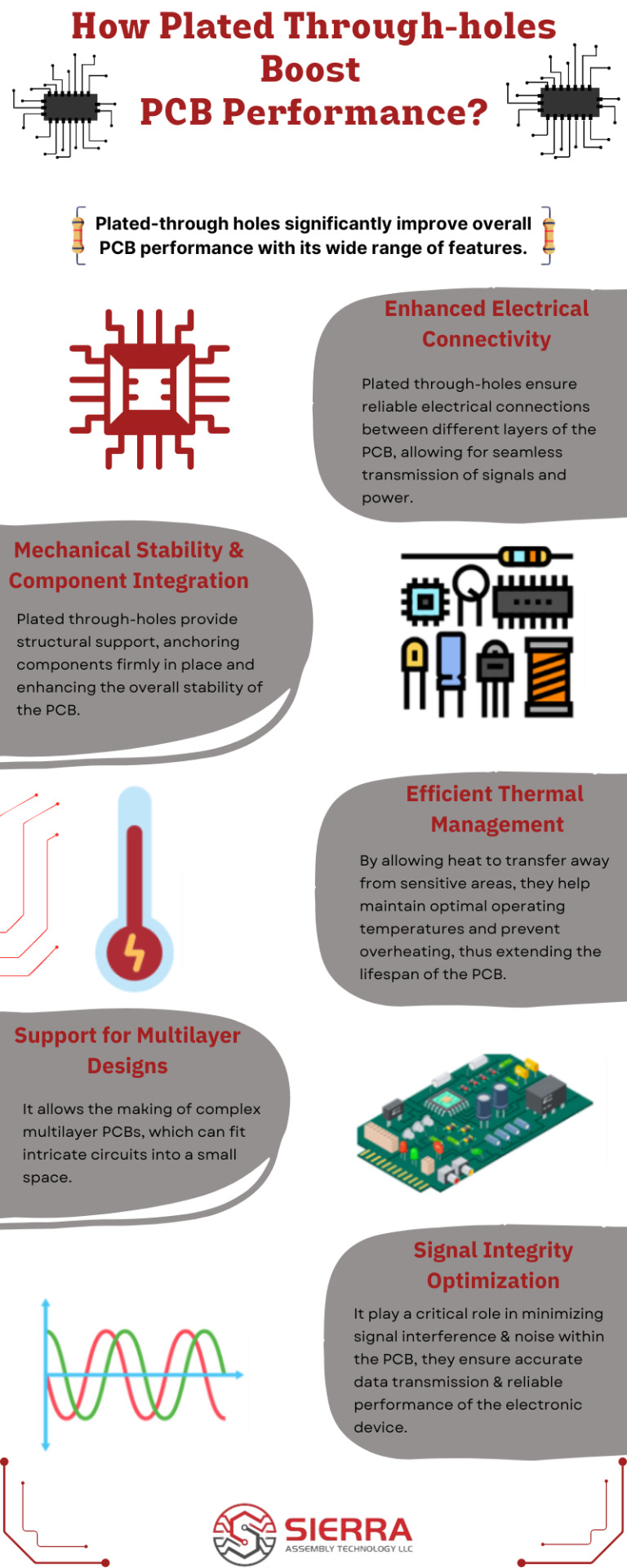
Plated through-holes (PTH) are holes that are drilled through the entire thickness of a printed circuit board (PCB) and have conductive material plated on their inner walls. Plated through-holes are a critical feature in PCB design, significantly enhancing the performance and reliability of the final product.
They ensure robust electrical connections across multiple layers, provide mechanical stability, assist in thermal management, and facilitate manufacturing and repair processes.
0 notes
Text
Through Hole PCB Assembly
THT PCB Assembly Manufacturer – One-stop service
What’s mean for Through Hole (THT) PCB Assembly and Surface Mount Technology(SMT)PCB Assembly ?
Surface Mount Technology (SMT) is necessary for PCB assembly. If the PCB has no through-hole components, Through Hole (THT) PCB Assembly is not needed.
SMT assembly: SMT stands for surface mount technology, which is a versatile PCB assembly technology. Currently, all electronic components can be made into surface-mounted devices (SMD). SMDs are interconnected to the PCB pads with solder paste. SMT assembly is automatic.
THT assembly: THT, or PTH or DIP, means through-hole technology. The electronic components that require THT assembly have long pins. Usually, they are capacitors, fuses, and connectors. The PCB is pre-drilled, and these components' pins plug in the holes and wave reflowed. THT assembly is manual.
In the PCB assembly process, SMT assembly happens before the THT assembly.

What are the benefits of Through Hole PCB assembly?
Through-Hole PCB Assembly comes with a range of benefits including:
Withstanding stress-As opposed to SMT components, through-hole components are known for their ability to withstand mechanical and environmental stress.
Perfect for large components-Through-hole works well for large components that have to undergo high power and high voltage
High heat tolerance-Known for their high heat tolerance, they find application in a number of industries, particularly military and aerospace.
Ease of Prototyping- Through-hole PCBs also lend themselves to ease of prototyping and improved reliability
High Reliability-Through-hole PCBs are best used for high-reliability products that require stronger connections between layers.
Little surprise then, that even though surface mount components allow for denser configurations, for larger and heavier components that require strong bonds, through-hole technology has remained resilient and relevant.
What are the capabilities you offer for Through Hole PCB assembly?
We provide through-hole PCB services to a variety of industries including medical, electronics, instrumentation, and military, all thanks to our complete assembly capabilities:
• Hand soldering
• Dual wave flow solder
• Hand Insertion of components
• Automate axial or radial insertion
• RoHS soldering using tin-lead solder
• Use of high and low melting point solder
• Prototype build to high-volume assembly
• Functional test and automated inspection
• Support various types of PCBs including metal core PCBs, Rigid PCBs, Flex-rigid PCBs, FR4 PCBs, etc.

Disadvantages of Through Hole Assembly
Like any other manufacturing or assembling techniques, Through Hole PCB Assembly has its disadvantages too.
These include:
Longer production time-It takes a lot of time to drill the multiple holes through which the leads are expected to run.
Expensive-because the drilling process is difficult and time-consuming, it increases the cost of production
Minimizes space on the boards-drilling the holes on the surface of the board limits the routing area for tracing signals.
Also, by feeding the leads through the board, only one of its sides is usable, thus making the THT PCB a bit slower in operation speeds.
Through Hole Assembly Components – What are the Best Components for Through Hole Assembly?
Radial lead components
Axial lead components.
Types of Through Hole PCB Assembly
There are two (2) main types of the Through Hole PCB Assembly. The first is the Automated Through Hole PCB Assembly. The second is the Manual Through Hole PCB Assembly.
On the one hand, the automated variant is roundly touted to be faster and cost-effective because it takes little time to be completed. It also demands little human inputs, which makes it cost-effective.
On the other hand, the manual Through Hole PCB Assembly involves the traditional or manually-operational model of drilling the holes into the Printed Circuit Boards (PCBs). This model tends to take time and attracts more costs.
Functional tests and automated inspection for Through Hole PCB Assembly
Using automated inspection is very critical in minimizing turnaround time to ensure timely delivery of the boards.
Conclusion
As you can see, Through Hole Assembly of PCB can be time consuming.
However, in some applications, it is worth it more so when mounting heavier and bulkier components.
You can easily achieve the strength by soldering the components on the reverse side as you have seen.
In fact, it is virtually impossible to pull components assembled using Through Hole Assembly.
The good news, today’s guide has simplified the Through Hole PCB Assembly technique.
Do you have questions or inquiries on Through Hole Assembly process?
Contact us now. [email protected]

In addition to through hole PCB assembly, we also provide value-added services, such as conformal coating, labeling, and complete PCB encapsulation.
Through-hole PCB Assembly Testing and Inspection at Hitechpcba
In-Circuit Testing:
This type of testing is conducted for high volume production lines, and helps us check every minute soldering and other components in detail.
Automated Optical Inspection: Abbreviated as AOI, these tests are performed to ensure that product is free from soldering, component, and BGA defects.
Automated X-Ray Inspection(AXI):
This testing is performed to inspect insufficient fills, short circuits, fills, etc. The automated X-ray inspection helps reduce the number of defects and improve the quality of the Through-Hole circuit.
Burn-in Tests:
These tests detect components’ failure or reliability in real environments.
Assisted Visual Inspection:
Our experts use a wide range of advanced visual inspection equipment to perform a detailed inspection of soldering and component placement accuracy.

What’s difference between SMT assembly and THT assembly?
Most contract PCB Assembly manufacturers concentrate on their surface mount technology capabilities for PCB assembly. The SMT lines can be almost completely automated making it possible to run a high volume of boards with little human intervention and a low cost per board. Through whole assembly whether automated or manual is a slower process, it takes resources away from the high-volume business that many manufacturers prefer.
Only about 10 percent of the parts we buy are through-hole. Nearly 75 percent of the boards we run are mixed technology, which is a combination of through-hole and SMT parts one reason for this is that nearly half of our board assemblies are for high powered boards which use capacitors inductors and transformers to transfer energy. The size of these components is proportional to the energy they can store so for a high-power board we need to use some fairly large and heavy components and that means through-hole technology, in addition things like customer accessible connectors, that have to withstand stress as cables are connected and removed are likely to be through-hole components. Through-hole components are held in place by the pins as well as the solder so you can get a much stronger and more reliable mechanical bond than with surface mount components that have only solder to hold them in place. If a contract manufacturer is focused on higher volume SMT business, it's important to understand how they will handle through-hole components when you need them at z-axis. We run mixed technology boards every day we have a modern stuff line with a paperless process for assembly instructions and assemble in a single piece flow from the stuff line to a wave solder to inline inspection, d-paneling, qc testing.
In addition to PCB Assembly, be it through hole or surface mount, at Hitech Circuits Co., Limited we also undertake PCB assembly rework offering complete reliability, high quality and optimal costs. Not only are we well-versed in inventory management, fabrication and process control, we also have a stringent control on vendor component management.
0 notes
Text
What is Heavy Copper PCB or Thick Copper PCB?
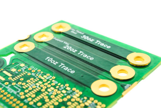
In high-power applications, managing ultra-high thermal loads and high-power currents is crucial. Standard PCBs typically have copper thicknesses ranging from 1oz to 3oz. However, in scenarios requiring robust current management and thermal dissipation, Heavy Copper PCBs, also known as Thick Copper PCBs, come into play. These boards have finished copper weights between 4oz and 10oz, with some super thick copper PCBs reaching 20oz to 200oz per square foot. The increased copper thickness enables these PCBs to handle high current outputs and optimize thermal management, crucial for electronics applications where temperature control is paramount to avoid performance degradation and premature failure.
Additionally, thick copper layers allow for large PCB cross-sections, which are ideal for high current loads, and facilitate heat dissipation. These PCBs also enable the integration of finely laid out structures on the outer layers with thick copper layers on the inner layers, providing a versatile solution for various design requirements.
Construction of Heavy Copper PCB
Manufacturing thick copper PCBs involves a combination of etching and electroplating processes, similar to standard PCBs. However, special techniques are required to ensure that trace sidewalls and undercuts meet the standards for thick copper features. Some of the main challenges in manufacturing thick copper PCBs include the need to remove a significant amount of copper during etching, increased etching costs, and the difficulty in manufacturing thin traces and ensuring the evenness of thick traces.
How to Make Thick Copper PCB?
The manufacturing process for thick copper PCBs involves several key steps to ensure the even thickness of the copper layers. These steps include etching inner layer traces on each layer of the inner core material, designing pads with uniform spacing and positioning, and using appropriate methods for burying copper in the prepreg. Common processes for thick copper PCBs include inserting thick copper bars into the circuit board, using laminate deposition with a thick base copper, and burying copper in the prepreg using laser cutting.
Advantages of Heavy Copper PCBs
Heavy Copper PCBs offer several advantages over standard PCBs:
Excellent high heat resistance: Heavy Copper PCBs can withstand high temperatures, making them ideal for high-power applications.
Improved current carrying capacity: The increased copper thickness allows Heavy Copper PCBs to carry larger currents with the same line width.
Reduced complex wiring: Heavy Copper PCBs can simplify complex wiring configurations, leading to more efficient designs.
Compression of board size: Heavy Copper PCBs allow for the integration of multiple copper weights on the same PCB, reducing the overall size of the end-use product.
Enhanced mechanical strength: The use of thick copper in PCBs improves the mechanical strength of the board, particularly in areas such as PCB connector areas and plated through holes (PTH).
Improved thermal management: Heavy Copper PCBs facilitate better heat dissipation, which is crucial for maintaining the performance and longevity of electronic components.
Ordinary PCB vs. Heavy Copper PCB
The main differences between standard PCBs and Heavy Copper PCBs lie in the manufacturing process and the copper weight. Standard PCBs are made through processes such as etching, hole drilling, and electroplating, while Heavy Copper PCBs require finer differential pair etching and step plating processes to ensure trace quality. Additionally, the copper content per square foot of a standard PCB is between 1oz and 3oz, whereas for Heavy Copper PCBs, the copper content exceeds 3oz.
Difference between Copper PCB and Heavy Copper PCB
Copper PCBs and Heavy Copper PCBs serve different purposes, with the main distinction being the thickness of the copper foil. Copper PCBs refer to PCBs with a copper substrate, which helps dissipate heat and prolong the life of components. On the other hand, Heavy Copper PCBs have a copper thickness exceeding 3oz and are used for their high current-carrying capacity.
Characteristics of Heavy Copper PCBs
Heavy Copper PCBs offer several unique features:
Ultra-high mechanical strength: Thick copper layers enhance the mechanical strength of the PCB, making it more resistant to weather and external stresses.
Excellent weather resistance: Heavy Copper PCBs can withstand extreme temperatures and harsh environmental conditions, ensuring the stability of the circuit transmission signal.
Thermal management: Thick copper layers improve heat dissipation, crucial for modern, high-density PCBs with high current loads.
Excellent current conduction: Heavy Copper PCBs provide excellent conductivity, facilitating the transmission of electricity between various components.
Diversity: Heavy Copper PCBs support various conductive and substrate materials, production processes, and application fields, making them versatile for different design requirements.
In conclusion, Heavy Copper PCBs play a crucial role in high-power applications where robust current management and thermal dissipation are essential. Their unique construction and characteristics make them ideal for applications requiring high heat resistance, excellent current carrying capacity, and improved thermal management.
High quality PCB manufacturer from China
0 notes
Video
tumblr
Need PCBs for your security, industrial control, or automotive electronics? PTH of PCB manufacturig Drilling is to drill the required vias in the copper clad PCB board. PCB vias are divided into plated holes ( PTH ) and non-plated holes (NPTH) according to whether they are metallized. According to the process, it is divided into blind holes of the PCB, buried holes and through holes. Vias mainly provide electrical connections and are used for fixing or positioning devices. Website: www.camtechcircuits.com [email protected]
0 notes
Text
Printed Circuit Board Surface Finishes: Advantages and Disadvantages
In the PCB industry, it is widely known that copper finishes are applied to the surface of circuit boards. Without proper protection, the copper can undergo oxidation and decay, rendering the PCB useless. The surface finish plays a crucial role as it serves two primary purposes: safeguarding the exposed copper circuitry and providing a solder-able surface for component assembly through soldering. Previously, Hot Air Solder Leveling (HASL) was considered a reliable method for achieving consistent assembly outcomes. However, the constant advancements in circuit complexity and component density have posed significant challenges for horizontal solder leveling systems, pushing them to their maximum capabilities. With the continuous reduction in component pitches and the increasing demand for thinner coatings, the use of Hot Air Solder Leveling (HASL) became a restrictive process for PCB manufacturers. Consequently, alternative coatings, including both electrolytic and immersion processes, have been available as substitutes for HASL for several years. Choose the best PCB manufacturing services in the USA for superior quality and reliable results.

Here are several frequently employed surface finishes in the realm of PCB manufacturing:
HASL / Lead Free HASL
In the PCB manufacturing industry, HASL stands as the prevailing surface finish. This widely adopted process involves submerging circuit boards into a molten tin/lead alloy, followed by the removal of excess solder using ‘air knives’ that blow hot air across the board’s surface. One notable advantage of the HASL process is its inadvertent ability to subject the PCB to temperatures reaching 265°C. This temperature exposure serves as an effective means of detecting any potential delamination issues well in advance, saving valuable resources before expensive components are affixed to the board.
Advantages
Affordable
Easily Accessible
Repairable
Exceptional Longevity
Disadvantages
Irregular Surface Texture
Limited Suitability for Fine Pitch Components
Includes Lead Content (HASL)
Susceptible to Thermal Shock
Risk of Solder Bridging
Potential Issues with Plugged or Reduced Plated Through Holes (PTHs)
Immersion Tin
As per IPC (Association Connecting Electronics Industry) guidelines, Immersion Tin (ISn) is a metallic finish applied through a chemical displacement reaction directly onto the copper base metal of a circuit board. This ISn coating effectively safeguards the underlying copper from oxidation throughout its intended shelf life. However, copper and tin possess a pronounced affinity for each other, leading to an inevitable diffusion process between the two metals. This interaction significantly affects the longevity of the ISn deposit and consequently impacts the overall performance of the finish. The adverse consequences associated with the growth of tin whiskers are extensively discussed in industry literature and form the subject matter of numerous published papers. Experience top-quality PCB manufacturing in the USA. Contact PCB Power Market now to bring your ideas to life!”
Advantages
Smooth Surface Texture
Lead-Free
Repairable
Preferred Option for Press Fit Pin Insertion
Disadvantages
Prone to Handling Damage
Involves Carcinogenic Substance (Thiourea)
Susceptible to Tin Corrosion on Final Assembly
Risk of Tin Whiskers Formation
Limited Suitability for Multiple Reflow/Assembly Processes
Challenging Thickness Measurement
Immersion Silver
Immersion silver is a chemical finish that does not require electrolysis and is applied by immersing the copper PCB into a silver ion solution. This surface finish is highly suitable for circuit boards requiring EMI shielding, as well as for applications involving dome contacts and wire bonding. The average thickness of the silver coating typically ranges from 5 to 18 microinches. In the context of modern environmental regulations like RoHS and WEE, immersion silver surpasses both HASL and ENIG in terms of environmental friendliness. Moreover, its popularity stems from its lower cost compared to ENIG, making it a cost-effective choice. Looking for reliable PCB manufacturing in the USA? Trust our expertise and precision. Get in touch with PCB Power Market today to discuss your project!”
Advantages
Offers Uniform Application Compared to HASL
Superior Environmental Profile Compared to ENIG and HASL
Comparable Shelf Life to HASL
Provides Cost Advantages over ENIG
Disadvantages
Requires Same-Day Soldering On PCB Removal from Storage
Prone to Tarnishing with Improper Handling
Lower Durability Compared to ENIG Due to Absence of Nickel Underlayer
OSP / Entek
OSP (Organic Solderability Preservative), also known as anti-tarnish, safeguards the copper surface from oxidation by employing a conveyorized process to apply an ultra-thin protective layer over the exposed copper. This process utilizes a water-based organic compound that selectively adheres to copper, forming an organometallic layer that shields the copper before soldering. Notably, OSP is exceptionally environmentally friendly when compared to other prevalent lead-free finishes, which tend to be either more toxic or require significantly higher energy consumption.
Advantages
Smooth Surface Texture
Lead-Free
Straightforward Process
Repairable
Cost-Efficient
Disadvantages
Difficult to Measure Thickness Accurately
Not Well-Suited for Plated Through Holes (PTH)
Shorter Shelf Life
Possible Implications for In-Circuit Testing (ICT)
Risk of Copper Exposure in Final Assembly
Demands Careful Handling
Original Source: https://primepositionseo.com/2023/06/08/printed-circuit-board-surface-finishes-advantages-and-disadvantages/
0 notes
Text

Double-side Flex-PCB Partial step:Shearing → Drilling → PTH → Electroless Plating → Pretreating → Dry Film Lamination → Position → Exposure → Develop → Pattern Plating → Remove Dry Film → Pretreating → Dry Film LaminationDouble-side Flex-PCB Partial step
#pcb#flex pcb#rigid-flex pcb#flex circuit pcb#flexible pcb board#flexible circuit board#fpcway#fpcway.com#www.fpcway.com#today on tumblr
0 notes