#Printed Circuit Board Terminal Blocks
Explore tagged Tumblr posts
Visit Tumblr Blog
Explore Tumblr blogs with no restrictions, modern design and the best experience.
Last Seen Tumblr Blogs


Fun Fact
69% of Tumblr users are millennials.
Text
A Simple Guide: Phoenix Contact Devices and Their Types
Technology keeps evolving, making electrical connections more reliable and efficient. Industries depend on high-quality connectors to ensure stable and secure connections in various applications. Phoenix Contact is known to provide advanced connection solutions for different industrial needs. From power distribution to automation, these devices help businesses maintain smooth operations. The top trading and contracting company in Muscat supplies Phoenix Contact devices, ensuring industries get reliable and durable connectors. In this article, we will discuss five types of Phoenix Contact device connectors and their uses.
Types of Phoenix Contact Device Connectors
PCB Terminal Blocks: PCB terminal blocks are essential for connecting wires to a printed circuit board. These connectors come in different sizes and designs to suit various industrial applications. They provide a secure and vibration-resistant connection, making them a reliable choice for automation systems and power electronics.
Heavy-Duty Connectors: Heavy-duty connectors are built to withstand harsh environments, including extreme temperatures, dust, and moisture. They are commonly used in industrial machinery, transportation, and power plants. Many businesses seek Phoenix contact distributors in Oman to get these connectors for their high durability and safety.
Circular Connectors: Circular connectors are widely used in automation and robotics. They offer a compact design with secure locking mechanisms, ensuring a stable connection in moving parts. These connectors are known for their excellent signal transmission, making them ideal for applications requiring continuous communication between devices.
Data Connectors: Data connectors ensure secure data transmission in industrial networks. They support Ethernet, USB, and fibre optic connections, allowing smooth communication between machines and control systems. These connectors play a key role in smart factories and automated production lines, improving efficiency and reliability. Their durable design helps industries maintain stable data flow, making them essential for modern industrial automation and networking solutions.
Power Connectors: Power connectors provide reliable power transmission in industrial setups. They ensure a stable electricity supply to various devices, reducing the risk of connection failures. These connectors are designed for high efficiency and durability, making them ideal for demanding applications. Many industries, including the top trading and contracting company in Muscat, choose these connectors for their superior performance and long-lasting quality, ensuring smooth and uninterrupted operations in industrial environments.
Wrapping UpPhoenix Contact devices offer advanced solutions for different industrial applications. Their wide range of connectors ensures safe and efficient electrical connections in various sectors. Businesses looking for high-quality connectors often rely on Phoenix contact distributors in Oman to meet their specific needs. With the right connectors, industries can improve efficiency and ensure reliable operations.
0 notes
Text
Comparing Reflow (THR/SMT) vs. Wave/Manual (THT) Soldering for Pluggable Terminal Blocks

Integrating terminal blocks into industrial applications requires careful consideration of the soldering process. Terminal blocks, which provide secure connections for electrical systems, come in two main forms: through-hole technology (THT) and surface-mount technology (SMT). These two methods involve different soldering techniques—wave/manual (THT) and reflow (THR/SMT). The choice of soldering process significantly impacts production speed, cost, and the overall quality of the finished product. Understanding the differences between these methods is crucial for manufacturers to make the right decisions for their assembly lines.
Differences Between THT (Wave/Manual) and THR/SMT (Reflow) for Industrial PCB Assembly
The primary difference between THT and SMT lies in how the terminal block is attached to the printed circuit board (PCB). THT involves inserting the terminal block’s pins through holes in the PCB, followed by soldering, usually via wave soldering or manual soldering. In contrast, SMT (including THR) places terminal blocks directly on the surface of the PCB, and soldering is typically done through a reflow process.
THT soldering is commonly used for larger, more robust terminal blocks, providing strong mechanical connections suitable for high-stress environments. SMT, on the other hand, is more suited for smaller, compact terminal blocks, offering high-density solutions and more automated assembly. Reflow soldering allows for precise control of temperature, reducing the risk of thermal damage to sensitive components, while wave soldering is more cost-effective for large-volume production, but it can be less accurate in comparison.
How Choosing the Right Process Affects Production Speed, Cost, and Quality The choice of soldering method directly impacts production speed, cost, and quality. THT (wave/manual) soldering is often slower and requires more manual labor, making it more expensive in smaller batches but effective for heavy-duty or high-reliability applications. Reflow soldering (THR/SMT) speeds up the production process with automation, making it more cost-efficient for mass production, though it may not provide the same level of mechanical robustness for certain heavy-duty applications.
In terms of quality, SMT soldering provides a cleaner finish with fewer defects such as cold solder joints, making it ideal for precision applications. THT soldering, on the other hand, excels in providing a stronger mechanical bond that is essential in demanding or high-vibration environments.
Best Practices
When choosing the best soldering method, manufacturers should consider factors like pin spacing and conductor entry designs. For THT soldering, larger pin spacings may be more appropriate for ease of manual or wave soldering, while tighter spacing in SMT applications allows for more compact, efficient designs.
In both cases, ensuring strong mechanical and electrical connections is vital. In harsh environments, terminal blocks must resist vibration, temperature fluctuations, and moisture, so selecting the right soldering method and design ensures reliable connections and long-lasting performance.
Conclusion
Choosing between reflow (THR/SMT) and wave/manual (THT) soldering for Pluggable Terminal Blocks is an important decision for manufacturers. Each method has its strengths and applications, with THT offering robust mechanical connections and SMT providing precise, efficient assembly. Manufacturers must carefully weigh production methods based on their specific needs, balancing speed, cost, and quality to achieve the best results for their terminal block integration.
0 notes
Text
Review, teardown, and testing of ERPF-400-24 Mean Well power supply
General Description

Brief Specification: ERPF-400-24 is a power supply unit with a 24-volt DC output and a rated current of up to 16.7 amps. According to the specification, the unit has an extended operating range for AC input voltage from 90 to 264 V. However, with an input voltage between 90 and 200 V, the unit can only deliver 50% of its rated power. It can also operate from a DC input within the range of 127 to 370 V.

The unit has dimensions of around 9x5x2 inches (220x130x48 mm exactly), is built on a printed circuit board housed in a stamped metal case, and is designed to operate with no forced cooling. The board is installed into the case, like in a tray, and is covered with a compound (most likely thermally conductive), making it non-removable for repair. The unit is covered with a perforated lid on top.
It features an LED indicator for output voltage and allows adjustment of the output voltage within a range of -5% to +10%. The unit includes an active PFC (Power Factor Correction) circuit and has a high power factor of up to 0.98 at 115 VAC. It also has thermal protection, with temperature monitoring performed using a thermistor placed on the output rectifier diodes. Traditional safe measures, such as overload and overvoltage protection, are also provided.
Circuit and construction description: Unfortunately, the compound filling makes detailed examination of the circuit difficult, so there is a high probability of interpretation errors. However, it appears that the design shares many similarities with the RSP-320-24 (https://teardownit.com/posts/review-teardown-and-testing-of-rsp-320-24-mean-well-power-supply) power supply unit, in both circuit and layout. This suggests that the ERPF-400 may be controlled by the FAN4800 controller, just like the RSP-320.
The input and output terminals are mounted on a common screw terminal block (1). The terminal block's connections from top to bottom are as follows: three terminals for phase, neutral, and ground (input), and three parallel terminals for the output, ground, and +24V. The input voltage from the terminal block (1) passes through an EMI filter (3) and then to the diode bridge (5). A varistor (2) is installed at the filter's input to suppress dangerous voltage spikes. The rectified voltage from the bridge (5) is then routed through an NTC inrush current limiter (4) to the active PFC circuit. The PFC's power stage consists of a transistor (6), inductor (11), diode (7), and output capacitor (8). The rectified and filtered voltage from capacitor (8) is fed into a forward converter, which comprises transistors (9) and transformer (10). The voltage from the transformer's output winding (10) is rectified by diodes (12) and filtered by an output LC filter (13) (14).
The filter’s output capacitance is provided by four 560µF, 35V capacitors rated for operation at up to 220°F or 105°C (13).
The transformer's core (10) is tied in a metal clamp, which is bolted to the case. This design likely serves to dissipate heat from the transformer.
Due to the presence of the compound, it is difficult to assess the overall build quality. The compound itself has been applied somewhat carelessly, with visible splatters and drips. Furthermore, there are gaps in the compound application, significantly reducing its protective effectiveness.


The LED output voltage indicator and output voltage adjustment resistor (16) are located near the terminal block, allowing access without removing the top cover.
Test Conditions
Most tests were conducted using Test Circuit 1 (see appendix) at 80°F (27°C), 70% humidity, and 29.8 inHg pressure. Unless otherwise specified, measurements were taken without pre-warming the power supply, and the operating mode was momentary load. Input voltage was set to 115V AC, and the current of 8.4 A was considered 100%. The following values were used to determine load levels:

Output voltage with static load

The unit demonstrates excellent output voltage stability.
Startup Characteristics
Startup at 100% load
Before the test, the power supply was turned off for at least 5 minutes with the load connected at 100%. The startup waveform at 100% load is shown below (Channel 1: output voltage, Channel 2: input current):

The startup process can be divided into three phases: 1. Input current pulses charging the input capacitors upon connection to the grid, with a peak amplitude of about 3 A, consisting of two portions of one period each. 2. Waiting for the control circuit to start, about 231 ms. 3. (Output Voltage Rise Time) Output voltage rise, 57 ms. 4. (Turn On Delay Time) The total time to reach operational mode from power-on is 288 ms.
(Output Voltage Overshoot) The startup process is aperiodic with no overshoot.
Startup at 0% load
Before the test, the power supply was turned off for at least 5 minutes with the load connected at 100%, then the load was disconnected, and the unit was turned on. The startup waveform at 0% load is shown below:
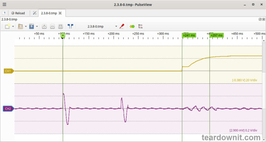
The startup process consists of three phases: 1. Input capacitors charging upon connection to the grid, with a peak amplitude of about 2.6 A, consisting of two portions of one period each. 2. Waiting for the control circuit to start, about 241 ms. 3. (Output Voltage Rise Time) Converter startup, output voltage rise, and transition to operational mode, 56 ms. (Turn On Delay Time) The total time to reach operational mode from power-on is 297 ms.
(Output Voltage Overshoot) The startup process is aperiodic with no overshoot.
Shutdown Characteristics
The shutdown process was tested at 100% load with nominal input voltage at the moment of shutdown. The shutdown waveform is shown below:

The shutdown process can be divided into two phases: 1. (Shut Down Hold Up Time) The unit continues operating, powered by the charge stored in the input capacitors, until their voltage drops to a critical level at which maintaining the output voltage is no longer possible. This phase lasts for 26 ms. 2. (Output Voltage Fall Time) Output voltage decline, converter stop, and acceleration of the voltage drop. This phase lasts for 25 ms.
(Output Voltage Undershoot) The shutdown process is aperiodic, with no undershoot.
Current amplitude at 100% load prior to shutdown was 2.8 A.
Output voltage ripple
At 100% load:
low-frequency ripple of about 10-12 mVp-p at twice the grid frequency, and around 4 kHz with a ripple of 13-15 mVp-p.

At the converter frequency, ripple is approximately 25 mVp-p, with noise at 120 mVp-p.

At 75% load:
low-frequency ripple of about 10 mVp-p at twice the grid frequency and around 12 mVp-p at approximately 4 kHz.

Converter frequency ripple is about 20 mVp-p, with noise at 100 mVp-p.

At 50% load:
low-frequency ripple of about 10 mVp-p at twice the grid frequency and around 15 mVp-p at approximately 4 kHz.

Converter frequency ripple is about 20 mVp-p, with noise at 100 mVp-p.

At 10% load:
low-frequency ripple of about 3-5 mVp-p.

Converter frequency ripple is about 20 mVp-p, with noise at 100 mVp-p.

At 0% load:
The input current was measured with a multimeter at 60 mA. (Power Consumption) Input current in this mode is primarily reactive in nature; thus, the power consumption value measured with handy instruments can't be correct. The input filter has two capacitors, according to the diagram.
At 0% load, low-frequency ripple is hardly distinguishable from the noise, about 3 mVp-p.

Converter frequency ripple is masked by noise around 100 mVp-p.

Dynamic characteristics
Dynamic characteristics were assessed in a mode that switches between 50% and 100% load. The oscillogram below illustrates the process:

It is evident that the unit's response to step-load changes is aperiodic, with the magnitude of the response to load changes being approximately 100 mV p-p.
Overload protection
The manufacturer specifies overload protection with a constant current limiting type, which was confirmed during testing. When overloaded or the output terminals are shorted, the unit enters current limiting mode and automatically recovers after the fault is removed.
The output current at which the limit is triggered is 22 A.
Input safety assessment
(Input Discharge) The input circuit discharge time constant was measured upon disconnection from the grid, with a value of 0.245 s. This means that when operating on a 120V grid, the time required for the input circuits to discharge to safe levels (<42 V) is 0.39 s:

Important: This result applies only to the tested unit and was obtained exclusively for research purposes. It cannot, under any circumstances, be considered a guarantee of safety.

The ground leakage current was measured at 73µA.
Thermal behavior
No significant heating of components was observed during no-load operation. Thermograms were taken at three power levels—80%, 90%, and 100%—with and without the top cover. The thermograms show that the most thermally loaded components of the unit are the NTC inrush current limiters (4), which stand out from the other components. At 80% load, the NTC temperature is 175.6°F (80°C, with a 53°C rise above ambient temperature); at 90% load, it reaches 192.1°F (89°C, with a 62°C rise); and at 100% load, it reaches 203.9°F (95.5°C, with a 68.5°C rise).
The second hottest component, after the NTC, is a resistor, 25 degrees cooler.
80% load
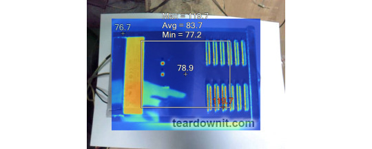

90% load


100% load


Conclusions
The ERPF-400-24 generally exhibits low noise and ripple, and it maintains good accuracy in sustaining the output voltage. The unit has decent dynamic characteristics, responding to pulsating loads without overshoot.
On the startup waveform (see oscillograms), there is an N-shaped section where, after the initial rise in output voltage, a partial drop occurs, followed by another rise and stabilization at the nominal level. This behavior could potentially cause issues when powering up digital devices that require initialization.
The build quality is good. However, the compound is applied somewhat poorly, with notable imperfections and several gaps. Unfortunately, these gaps affect components with increased hygroscopicity, particularly the wire-wound inductances of the output and input noise filters. Despite the manufacturer's claim of “protecting the internal electronic components from rain splash and dust,” this unit should not be used without additional water ingress protection.
According to the specifications, the unit is designed for operation under conditions of "Cooling by free air convection" and "-22F ~ +140°C (Refer to output load derating curve)." The tested unit indeed remains safe up to 100% load during continuous operation. The presence of a temperature sensor on the rectifier diodes adds extra assurance of safety.
Important: The results and conclusions presented apply only to the tested unit and were obtained solely for research purposes. Under no circumstances should they be used to assess all devices of this type.
0 notes
Link

#Meter-terminal-parts#meter-Terminal-Blocks#Brass Terminal Blocks#Printed Circuit Board Terminal Blocks#Regular Duty Terminal Blocks#Heavy Duty Terminal Blocks#Euro Style Terminal Blocks#Modular Terminal Blocks#Pluggable Terminal Blocks#Italy
0 notes
Text
“The Importance of IC Sockets and Terminal Blocks in Electronic Design”
IC sockets are old to securely mount ICs onto a printed undefined board (PCB) without the want for soldering. This makes it easy to replace a faulty IC or upgrade the circuit without damaging the PCB. Sockets also allow for testing and prototyping of circuits before final assembly. They come in various sizes and configurations to accommodate different Intelligence Community packages.
0 notes
Photo

Buy Printed circuit board terminal with Lowest Price @ Campus Component. It gives you highly dependable connections without the need for wire lugs. Terminal Blocks are in stock at Campus Component from industry leading manufacturers. Huge Selection of Terminal Blocks In Stock with No Minimum Order & Fast Delivery!. For more details Visit https://www.campuscomponent.com/products/printed-circuit-board-terminal-mkds-3-2-5-08-1711725-tb-2348-d/2208614000009206267
0 notes
Text
wanjie-tb.com
A terminal block (also called as connection terminal or terminal connector) is a modular block with an insulated frame that secures two or more wires together. It consists of a clamping component and a conducting strip. Due to the terminal connection, the joint of the wire can be kept proper and secure. And the wire can also be properly aligned. Terminal blocks can be classified on the basis of their structure, device type, termination options.
PCB screw terminal blocks are modular, insulated devices that mount on printed circuit boards (PCBs) and secure two or more wires together. PCB terminal block connector also known as electronic blocks, are manufactured to be mounted on a printed circuit board, or PCB. Terminal blocks are used to secure and/or terminate wires and, in their simplest form, consist of several individual terminals arranged in a long strip.
Screwless terminal blocks have spring terminals that automatically grip inserted wires and release when their levers are pressed, enabling easy, temporary connections to a PCB. Various sizes are available in two orientations (side-entry and top-entry) and two pin spacings (0.1″ and 0.2″). These terminal blocks can be combined to make longer ones, or segments can be removed to make them shorter. Each block has two pins per terminal, and they are intended for use with PCBs that have the appropriate footprints.
MCS terminal block uses high-elastic and high-quality spring clips for single-strand and multi-strand connections. The characteristic is safe, fast, and reliable and it is suitable for wire-to-wire, board-to-wire and board-to-board connections to achieve power and signal transmission.
Feed-through terminal blocks are characterized by two terminal points and a compact design. Ground terminals of the same shape are available to match the feed-through terminal blocks. All bridgeable terminal blocks can be bridged together easily with multi-conductor and function terminals. A feed-through terminal block is suitable for joining and/or connecting one or more conductors. They could have one or more connection levels that are on the same potential or insulated against one another.
The barrier terminal block is designed for power applications and integrates a transparent clamshell safety cover. Barriers can tolerate cluttered or worn wire ends to prevent electrical shorts between positions on the same terminal block and adjacent components. There are a variety of high-quality barrier-style terminal blocks in single-row, double-row, and high voltage options to fit a variety of applications. The barrier terminal blocks (sometimes called barrier terminals or barrier strips) are built with sturdy, thermoplastic materials to make them break-resistant and heat-resistant.
DIN rail terminal blocks are used to protect electrical systems against overcurrent and short-circuiting. They clip onto a DIN rail, which is a standard-size metal rail on which terminals are mounted in a control cabinet. DIN rail terminals are made from plastic, as this insulates the electrical current running through the terminal. Fused DIN rail terminals often have a hinged section containing the fuse, which can be opened up to stop the flow of electricity. Some are fitted with an LED blown fuse indicator to let you know when the fuse needs changing. Fused DIN rail terminals come with different fuse size inserts and may be color-coded to indicate the current rating. Non-fused work the same, just without the fuse protection.
A circular connector is a cylindrical, multi-pin electrical connector that contains contacts that power electrical devices, transmit data, or transmit electrical signals. A circular connector is designed to withstand harsh environments and reliably deliver data. It is designed with a circular interface and housing to quickly and easily connect and disconnect signal, power, and optical circuits without the use of coupling tools such as torque wrenches. The contacts are typically surrounded by a composite or metal shell and are embedded in insulating material to maintain their alignment. The contacts are usually paired with a cable, making them especially resistant to accidental decoupling or environmental interference.
A breadboard is used to build and test circuits quickly before finalizing any circuit design. The breadboard has many holes into which circuit components like ICs and resistors can be inserted. The holes are most commonly spaced 0.1“ apart to accommodate standard DIP components. The breadboard has strips of metal sockets that run underneath the board and connect the groups of five holes on the board.
A jumper wire (also known as jumper, jump wire, DuPont wire) is an electrical wire, or group of them in a cable, with a connector or pin at each end (or sometimes without them – simply "tinned"), which is normally used to interconnect the components of a breadboard or other prototype or test circuit, internally or with other equipment or components, without soldering. Individual jump wires are fitted by inserting their "end connectors" into the slots provided in a breadboard, the header connector of a circuit board, or a piece of test equipment.
0 notes
Text
Review, teardown, and testing of RS-150-24 Mean Well power supply
General description

A short description. The RS-150-24 is a power supply with a constant output voltage of 24 volts and a current of up to 6.3 amperes. According to the specification, the unit has two AC input voltage operating ranges—from 88 to 132 and 176 to 264 volts. Range selection is non-automatic with a mechanical switch. The supply measures close to 7.5 × 4.0 × 1.5 inches (192 × 98 × 38 millimeters) and is made on a printed circuit board fixed to the base of the metal case, designed to operate with passive cooling. The top lid covering the case is perforated. The power supply has an LED indication for the output voltage, allowing one to adjust it within -5 to +10%. This unit does not have either PFC or thermal protection.
Design description. The input and output circuits of the power supply are connected to a common screw block (1). From left to right, there are three terminals for the input line, neutral and ground wires, and two parallel blocks of two terminals for the outputs: ground and +24V. The input voltage from the screw terminals through the fuse (2) is supplied to the RF interference filter (3) and then goes to the diode bridge (5). A varistor (4) is installed at the filter input to suppress hazardous pulses. The rectified voltage from the bridge (5) through the range selector (6) and through two NTC inrush current limiters (7) is supplied to the input electrolytic capacitors (8). Rectified and filtered voltage from capacitors (8) goes to the forward converter, which consists of a NE1101 controller (9, on the back side of the board), a 2SK3878 power N-MOSFET transistor (10), and a transformer (11). The voltage from the output winding of the transformer (11) is rectified by the fast-recovery diode 20F20SAB3 (12) and filtered using an output LC filter (13) (14).
The base resistance of each NTC is about 4.5 Ohms.
Output filter capacitance: 2 pieces of 470 uF, 35 volts, designed for operating temperatures up to 220℉ (105℃) (14).
The output voltage is stabilized by shunt regulator AS431ANTR-E1, transmitting the control signal to the high-voltage side of the circuit through the 817C transistor optocoupler (15). A second optocoupler of the same type forms a bypass channel for overvoltage protection (OVP).
The rectifier bridge (5), transistor (10), and diode (12) are installed with individual heat sinks, which (10, 12) are pushed against the housing with screws. Between the aluminum case and the board (from the solder side) is an extra insulation layer, a thin fiberglass sheet. All bulky components are additionally fixed using a compound.
Build quality is good. The board has empty spaces for installing an additional parallel diode (12) and three output electrolytic capacitors. The board is obviously unified for all the models in the series, and these elements are used in lower-voltage models.
The output voltage LED indicator (16) and the output voltage adjustment resistor (17) are located near the terminal block so that they can be accessed without removing the top cover.
Test conditions
Most tests are performed using Metering Setup #1 (see appendices) at 80℉ (27℃), 70% humidity, and 29.8 inHg pressure. Unless mentioned otherwise, the measurements were performed without preheating the power supply with a short-term load. The following values were used to determine the load level:

Output voltage under a constant load

The high stability of the output voltage should be noted.
Power-on parameters
Powering on at 100% load
Before testing, the power supply is turned off for at least 5 minutes with a 100% load connected. The oscillogram of switching to a 100% load is shown below (channel 1 is the output voltage, and channel 2 is the current consumption from the grid):

On the oscillogram, three phases of the starting process can be distinguished: 1. Two pulses of the input current charging the input capacitors when connected to the grid have an amplitude of about 14.5 A and a duration of about one main voltage period. 2. Waiting for the power supply control circuit to start for about 220 ms. 3. (Output Voltage Rise Time) Output voltage rise takes 5 ms. (Turn On Delay Time) The entire process of entering the operating mode from the moment the device powers on is 228 ms.
(Output Voltage Overshoot) The switching process is aperiodic; there is no overshoot.
Powering on at 0% load
The power supply is turned off at least 5 minutes before the test, with a 100% load connected. Then, the load is disconnected, and the power supply is switched on. The oscillogram of switching to a 0% load is shown below:

The picture shows three distinguishable phases of the power-on process: 1. Charging the input capacitors when connected to the grid has an amplitude of about 14.5 A. 2. Waiting for the power supply control circuit to start for about 228 ms. 3. (Output Voltage Rise Time) Starting the converter, increasing the output voltage, and entering the operating mode takes 5 ms. (Turn On Delay Time) The entire process of entering the operating mode from the moment the device powers on is 233 ms.
(Output Voltage Overshoot) The switching process is aperiodic; there is no overshoot.
Power-off parameters
The power supply was turned off at 100% load, and the input voltage was nominal at the moment of powering off. The oscillogram of the shutdown process is shown below:

The oscillogram shows two phases of the shutdown process: 1. (Shutdown Hold-Up Time) The power supply continues to operate because the input capacitors hold charge until the voltage across them drops to a certain critical level, at which point maintaining the output voltage at the nominal level becomes impossible. The phase takes 38 ms. 2. (Output Voltage Fall Time) Reduction of the output voltage, stopping voltage conversion, and accelerating the voltage drop takes 33 ms.
(Output Voltage Undershoot) The shutdown process is aperiodic; there is no undershoot.
The amplitude of the current at 100% load before shutting down is 5.7 A.
Output voltage ripple
100% load
At 100% load, the low-frequency ripple is approximately 3 mV.

At 100% load, the ripple at the converter frequency is approximately 40 mVp-p, and the noise is 100 mVp-p.

75% load
At 75% load, the low-frequency ripple is approximately 4 mV.

At 75% load, the ripple at the converter frequency is approximately 40 mVp-p, and the noise is 100 mVp-p.

50% load
At a 50% load, the low-frequency ripple is approximately 3 mV.

At 50% load, the ripple at the converter frequency is approximately 25 mVp-p, and the noise is 100 mVp-p.

10% load
At 10% load, the low-frequency ripple is approximately 3 mV.

At a 10% load, the ripple at the converter frequency is approximately 40 mVp-p, and the noise is 100 mVp-p.

0% load
No-load current consumption measured with a multimeter: 68 mA. (Power Consumption) The current consumption in this mode is predominantly reactive, so it isn't easy to reliably measure it with a basic set of instruments. The power supply's input filter contains two capacitors with a combined capacitance of approximately 1 uF.
At 0% load, the low-frequency ripple is indistinguishable from background noise of approximately 2 mVp-p.

At 0% load, the ripple at the converter frequency is masked by the background noise of approximately 50 mVp-p.

Dynamic characteristics
A mode with periodic switching between 50% and 100% load was used to evaluate the dynamic characteristics. The oscillogram of the process is shown below:

It is evident that the supply’s response to abrupt load changes is aperiodic; the magnitude of the response to load changes is about 100 mV p-p.
Overload protection
The claimed protection type is "hiccup mode, which recovers automatically after the fault condition is removed." This was confirmed during testing. When a short circuit occurs, the power supply periodically tries to turn back on and, if the overload is still present, turns off again until the next attempt.
The output current for the overload protection to kick in is 8.8 A.
Input circuit safety assessment
(Input discharge) Safety assessment is based on the discharge time constant of the input circuits when disconnected from the grid; the value is 0.234 s. This means that when operating on a 120 V input voltage, the time required to discharge the input circuits to safe values (<42 V) will be 0.652 s:

Important: The result is valid for this particular power supply unit; it was obtained for testing purposes and should not be taken as a safety guarantee.

The leakage current at the ground pin is 29 µA.
Thermal conditions
When operating with no load connected, no component overheating had been noticed. Thermograms were captured at three power levels: 80, 90, and 100%, fully assembled and with the lid removed. Thermal images show that the most loaded element of the block are four ballast resistors that shunt the source output, which are located near the inductance of the output LC filter (13) and whose heating noticeably stands out against the background of other components. At 80% load, they heat up to 219℉ (104℃, 139℉ above ambient temperature). At 90%, it's 233℉ (112℃, 153℉ above ambient), and at 100%, it reaches 239℉ (115℃, 159℉ above ambient). It is worth noting here that overheating increases faster than output power.
80% load


90% load


100% load


Conclusions
RS-150-24 generally has little noise and ripple, the output voltage is maintained accurately, and the build quality is solid. The power supply's dynamic characteristics are fine; the unit reacts to a pulsing load with no overshoot.
According to the specification, it is designed for “cooling by free air convection” and “high operating temperatures up to 70°C.” However, our test unit at 100% load heated up its load resistors up to 320℉ (160℃), which seems dangerous. For long-term operation, the load should be limited to 70–80% of the nominal one, especially during the hot season when ambient temperatures reach 95℉ (35℃) or more.
When assessing the safety of the operation of such a power supply, it is necessary to consider the possibility that the load exceeds the rated value due to malfunction but remains below the protection trigger level. In this case, the output power for the tested unit will be 135% of the nominal value, leading to even greater overheating, resulting in power supply failure and a fire hazard.
Important: The results are valid for this particular power supply unit; they were obtained for testing purposes and should not be used to evaluate all the units of the same type
0 notes
Link

#Brass Terminal Blocks#Printed Circuit Board Terminal#Blocks#Regular Duty Terminal Blocks#Heavy Duty Terminal Blocks#Euro Style Terminal Blocks#Modular Terminal Blocks#Pluggable Terminal Blocks#Italy
0 notes
Text
"The Importance of IC Sockets and Terminal Blocks in Electronic Design"
Integrated circuits (ICs) are the building blocks of Bodoni font electronic devices. These tiny chips can contain millions of transistors, allowing for undefined functionality in a small form factor. However, ICs are not standalone components - they require connections to unusual components in the circuit to operate properly. This is where IC sockets and terminal blocks come in.
IC sockets are old to securely mount ICs onto a printed undefined board (PCB) without the want for soldering. This makes it easy to replace a faulty IC or upgrade the circuit without damaging the PCB. Sockets also allow for testing and prototyping of circuits before final assembly. They come in various sizes and configurations to accommodate different Intelligence Community packages.
Terminal blocks, on the strange hand, are used to connect wires or unusual components to the undefined board. They supplya procure and reliable connection that can be easily disconnected when necessary. Terminal blocks come in many shapes and sizes, from single-terminal strips to multi-position blocks, and can handle a straddle of current and electromotive force ratings.
The use of United States Intelligence Community sockets and terminal blocks in electronic design has some benefits. Firstly, they offer flexibility and ease of use during prototyping and testing. With sockets, designers can switch out ICs or qualify circuits without damaging the PCB, which savesclock and money in the long run. Terminal blocks also make it easy to connect and unplug wires or components, reducing the risk of damage or short-circuit circuits.
Another advantage is the cleared reliability of the final product. National Intelligence Community sockets ensure that the IC is securely affixed and protected from mechanical stress, reducing the likeliness of unsuccessful personsundefined to physical damage. Terminal blocks provide a robust and steady-going connection that puts upresistance to environmental factors such as temperature changes and vibration.
Furthermore, the use of IC sockets and depot blocks can streamline the meeting place process. With pre-mounted sockets and terminal blocks, the time and effort required for hand-soldering or wire-wrapping connections are eliminated. This can result in quicker assembly multiplication and improved production efficiency.
In conclusion, IC sockets and terminal blocks play a material role in Bodoni font electronic design. They offer flexibility, ease up of use, improved reliability, and streamlined assembly processes. As such, designers should carefully look at the use of these components in their electronic circuits to optimise their plan and ensure the highest level of performance and reliability.
0 notes
Text
Touch Screen Technology Application and Classification
With the development of computer technology, the input method of the computer has gone from the original paper tape input to the keyboard input, to the mouse input, and then to the touch input, which has gone through four stages. This process is a process from professional to popularization. Touch screen technology allows more people to use the computer.
A touch screen is an interactive input device. The user only needs to touch a certain position on the screen with a finger or a light pen to control the operation of the computer. Therefore, the touch screen technology has the characteristics of simple operation and flexible use.
Touch screen is also called touch panel. When the graphic buttons on the screen are touched, the haptic feedback system on the screen can drive various linking devices according to a pre-programmed program, which can be used to replace the mechanical button panel and create a dynamic audio-visual effect by the LCD. Simply put, it is an inductive display device that can be connected to input signals such as contacts.
The application scenarios and terminals of touch screens are very extensive, and they can be divided into 7 categories from the perspective of scene types:
Type 1: Portable Equipment
Including Mobile phone, Pocket PC, E-book, Web Pad, Translator, Tablet PC, etc.
Type 2: Public Information Equipment
Including ATM, Public Inquiry Machine (Kiosk), Ticket Vending Machine, Digital Photo Printing System, etc.
Type 3: Communication Equipment
Including Video Phone, SmartPhone, Internet TV, Set-top box, GPS, etc.
Type 4: Office Automation Equipment
Including Copier, Punch Card Machine, Word Processor, Electronic Touch Whiteboard, etc.
Type 5: Information Collection Equipment
Including POI, POS Information Inquiry Machine, etc.
Type 6: Information Appliances
Including Refrigerator, Microwave, Coffee Maker, Washing Machine, LCD TV, etc.
Type 7: Entertainment Devices
Including Gaming Machine, Gambling Machine, Slot machine, Roulette machine, etc.
According to the type of sensor, touch screens are roughly divided into five types: infrared, resistive, surface acoustic wave(SAW), capacitive touch screens, and electromagnetic touch screens.
Infrared technology touch screens are inexpensive, but the outer frame is fragile, which is prone to light interference and distortion in curved surfaces. The design of capacitive technology touch screens is reasonable, but it is difficult to solve the problem of image distortion. The positioning of resistive technology touch screens is accurate, but its The price is quite high, and it is afraid of scratching; the surface acoustic wave touch screen solves the various defects of the previous touch screen, and it is not easy to be damaged. It is suitable for various occasions. The disadvantage is that if there are water droplets and dust on the screen surface, the touch screen will become dull It doesn't even work; electromagnetic technology touch requires a professional stylus, which is inconvenient to use.
1.Infrared touch screen
The principle of the infrared touch screen is very simple, just add the frame frame of the light spot distance on the display, without adding a coating or connecting the controller to the surface of the screen. Infrared emitting tubes and receiving tubes are arranged on the four sides of the frame from the light spot to form an infrared network on the screen surface. When the user touches a certain point on the screen with his finger, the two infrared rays passing through the position are blocked, and the computer can immediately calculate the position of the touched point. Because the infrared touch screen is not affected by current, voltage and static electricity, it is suitable for some harsh environmental conditions. Its main advantages are low cost, easy installation, no need for cards or any other controllers, and it can be used on computers of all grades. However, since the frame is only added to the ordinary screen, the infrared emitting tube and the receiving tube around the frame are easily damaged during use.
2.Resistive touch screen
The surface touched by the finger is a hard coating to protect the underlying PET layer. The PET layer is a thin elastic PET film that bends downward when the surface is touched, and allows the two underlying ITO coatings to contact each other and connect the circuit at that point. Between the two ITO layers is a separation fulcrum about one thousandth of an inch thick that separates the two layers. At the bottom is a transparent hard bottom layer to support the above structure, usually glass or plastic.
3.Surface Acoustic Wave(SAW) touch screen
A surface acoustic wave is a mechanical wave that propagates along the surface of a medium. The touch screen is composed of a touch screen, a sound wave generator, a reflector and a sound wave receiver. The sound wave generator can send a high frequency sound wave across the surface of the screen. When a finger touches the screen, the sound wave on the contact point is blocked Determine the coordinate position. The surface acoustic wave touch screen is not affected by environmental factors such as temperature and humidity. It has extremely high resolution, excellent scratch resistance, and long life (50 million times without failure); high light transmittance (92%), which can maintain clear and translucent Image quality; no drift, only need to be corrected once during installation; there is a third axis (ie pressure axis) response, which is most suitable for use in public places.
4.Electromagnetic touch screen
The basic principle of the electromagnetic induction touch screen is to judge by the magnetic field generated by the sensor under the panel during the operation of the electromagnetic pen. The electromagnetic pen is the signal transmitter, and the antenna board is the signal receiver. When a change occurs, the position point is defined by the operation.
5.Capacitive touch screen
Capacitive touch screens are divided into surface capacitive touch screens and projected capacitive touch screens.
(1) Surface Capacitive Technology:
The surface capacitive touch screen uses only a single layer of ITO, and long and narrow electrodes are plated on all four sides of the touch screen to form a low-voltage AC electric field within the conductor. When a finger touches the screen surface, a coupling capacitance is formed between the finger and the conductor layer, and a certain amount of charge is transferred to the human body. In order to recover these charge losses, the charge is replenished from the four corners of the screen, and the amount of charge replenished in all directions is proportional to the distance of the touch point, from which we can calculate the position of the touch point.
(2) Projected Capacitive Technology:
Compared with surface capacitive touch screens, projected capacitive touch screens can penetrate a thicker cover layer and do not require correction. Inductive capacitive etching of different ITO modules on two layers of ITO coating requires consideration of factors such as the total impedance of the module, the impedance of the connecting line between the modules, and the parasitic capacitance generated at the intersection of the two layers of ITO modules.
Which of the five touch screens do you like best? And which one is the best choice?Please follow our next article to learn more!
0 notes
Link
Pluggable Connectors Wholesale Suppliers in India
The right solution for every application: Whether on the printed circuit board, in the control cabinet or for lighting connection, Chawla Electronic pluggable connectors quickly and easily connect to the widest variety of applications.
Pluggable Terminal Blocks are available at Chawla Electronic.
Chawla Electronic is an authorized distributor for many pluggable terminal blocks manufacturers including Vital Electrocomp, Altech, Amphenol, FCI, Molex, Phoenix, TE Connectivity and more. Please view our large selection of
pluggable connector
products below:
COM ST/14 M
COM ST/14 F RSL
COM ST/12 M
COM ST/8 F RSL
#pluggable connectors#pluggable connectors wholesale supplier#pluggable connector suppliers#connectors#pluggable wholesale suppliers#chawla electronic#electronic products
0 notes
Text
Review, teardown, and testing of RSP-150-24 Mean Well power supply
General description

A short description
The RSP-150-24 is a universal input power supply with a constant output voltage of 24 volts and a current of up to 6.3 amperes. According to the specification, it has an operating AC input voltage range of 85 to 370 volts without manual switching. The supply measures close to 7.8 × 3.9 × 1.2 inches (199 × 99 × 30 millimeters) and is made on a printed circuit board fixed to the base of the metal case, designed to operate with passive cooling. The top lid covering the case is perforated.
The power supply has an LED indication for the output voltage and allows one to adjust it within -5 to +10%. This unit does not have either PFC or thermal protection.
Design description
The input and output circuits of the power supply are connected to a common screw block (1). From left to right, there are three terminals for the input line, neutral, and ground wires, and two parallel blocks of two terminals for the outputs: ground and +24V.

The input voltage from the screw terminals is supplied to the RF interference filter (2) and through the fuse (3) to the diode bridge (5). Next, the rectified voltage is supplied to the active PFC, controlled by the PFC+PWM controller FAN4800 (4). The power part of the PFC is assembled using a MOSFET 19NM50N (6) and an 8A 600V ultrafast diode STTH8S06D (7). The output voltage from the PFC is supplied to the two-transistor forward converter, whose transistors, 14NM50N (9), are controlled by the same controller, FAN4800. The converter voltage from the transformer (10) is supplied to the rectifier and to the LC filter (13, 14). The output rectifier is made using MBR20150 diodes (12). The filter output capacitance is 470 uF, 35 V, designed for operating temperatures up to 220F (105C) (14).
General stabilization control is performed by the AP4310 chip. The control signal is transmitted from it to the high-voltage part of the circuit through a transistor optocoupler (15). One optocoupler serves as the main regulation channel, the second forms a backup channel for overvoltage protection (OVP), and the third provides reception of a remote control signal.
To limit the inrush current, there is an NTC (18) connected to the output stage of the rectifier bridge (5) near the boost inductor PFC.
The rectifier bridge (5), transistors, and diodes (6, 7, 9, and 12) are pushed against the housing with screws using overhead metal strips. Between the aluminum case and the board (from the solder side), there is an extra insulation layer, a thin sheet of fiberglass. All bulky components are additionally fixed using compound.
Build quality is good.
Test conditions
Most tests are performed using Metering Setup #1 (see appendices) at 80F (27C), 70% humidity, and 29.8 inHg pressure.
The measurements were performed without preheating the power supply with a short-term load, unless mentioned otherwise.
The following values were used to determine the load level:

Output voltage under a constant load

The high stability of the output voltage should be noted.
Power-on parameters
Powering on at 100% load
Before testing, the power supply is turned off for at least 5 minutes with a 100% load connected.
The oscillogram of switching to a 100% load is shown below (channel 1 is the output voltage, and channel 2 is the current consumption from the grid):

The picture shows three distinguishable phases of the power-on process:
1. The pulse of the input current charging the input capacitors when connected to the grid has an amplitude of about 4.5 A and a duration of about 5 ms.
2. Waiting for the power supply control circuit to start for about 50 ms.
3. (Output Voltage Rise Time) Output voltage rise takes 6 ms.
(Turn On Delay Time) The entire process of entering the operating mode from the moment of powering on is 61 ms.
(Output Voltage Overshoot) The switching process is aperiodic; there is no overshoot.
Powering on at 0% load
The power supply is turned off for at least 5 minutes before the test, with a 100% load connected. Then the load is disconnected and the power supply is switched on.
The oscillogram of switching to a 0% load is shown below:

The picture shows three distinguishable phases of the power-on process:
1. Charging the input capacitors when connected to the grid has an amplitude of about 1.5 A.
2. Waiting for the power supply control circuit to start for about 27 ms.
3. (Output Voltage Rise Time) Starting the converter, increasing the output voltage, and entering the operating mode take 4 ms.
(Turn On Delay Time) The entire process of entering the operating mode from the moment of powering on is 31 ms.
(Output Voltage Overshoot) The switching process is aperiodic; there is no overshoot.
Power-off parameters
The power supply was turned off at 100% load, and the input voltage at the moment of powering off was nominal. The oscillogram of the shutdown process is shown below:

The oscillogram shows two phases of the shutdown process:
1. (Shutdown Hold-Up Time) The power supply continues to operate due to the input capacitors holding charge until the voltage across them drops to a certain critical level, at which maintaining the output voltage at the nominal level becomes impossible. The phase takes 20 ms.
2. (Output Voltage Fall Time) Reduction of the output voltage, stopping voltage conversion, and accelerating the voltage drop take 6 ms.
(Output Voltage Undershoot) The shutdown process is aperiodic; there is no undershoot.
The current waveform at 100% load right before shutdown is close to sinusoidal with an amplitude of 2 A.
Output voltage ripple
100% load
At 100% load, the low-frequency ripple is approximately 15 mV.

At 100% load, the ripple at the converter frequency is approximately 50 mVp-p, and the noise is 70 mVp-p.

75% load
At 75% load, the low-frequency ripple is approximately 10 mV.

At 75% load, the ripple at the converter frequency is approximately 20 mVp-p, and the noise is 30 mVp-p.

50% load
At a 50% load, the low-frequency ripple is approximately 6 mV.

At 50% load, the ripple at the converter frequency is approximately 30 mVp-p, and the noise is 50 mVp-p.

10% load
At a 10% load, the low-frequency ripple is approximately 10 mV.

At a 10% load, the ripple at the converter frequency is approximately 30 mVp-p, and the noise is 50 mVp-p.

0% load
No-load current consumption measured with a multimeter: 29 mA.
(Power Consumption) The first assumption of excessive standby power draw of more than 6.5 watts is wrong, since the current in this mode is predominantly reactive. Indeed, the input filter in the circuit contains two capacitors with a combined capacitance of 1.5 μF.
Measuring the exact active power consumption at a 0% load with a basic set of instruments (oscilloscope, multimeter, etc.) is not possible.
At 0% load, the low-frequency ripple is approximately 2 mV.

At 0% load, ripples at the converter frequency are masked by the 80 mVp-p noise.

Dynamic characteristics
To evaluate the dynamic characteristics, a mode with periodic switching between 50% and 100% load was used. The oscillogram of the process is shown below:

It is clear that the power supply, when the load changes abruptly, allows for a slight dampening overshoot; the magnitude of the response to load changes is about 260 mV.
Overload protection
The claimed protection type is "constant current limiting, recovers automatically after the fault condition is removed." This was confirmed during testing. When the output is overloaded or shorted, the unit goes into current stabilization mode and automatically restores operation when the overload goes away.
The output current for the overload protection to kick in is 7.9 A.
Input circuit safety assessment
(Input discharge) Safety assessment is based on the discharge time constant of the input circuits when disconnected from the grid; the value is 0.126 s. This means that when operating on a 120 V input voltage, the time required to discharge the input circuits to safe values (<42 V) will be 0.2 s:

Important: The result is valid for this particular power supply unit; it was obtained for testing purposes and should not be taken as a safety guarantee.

The leakage current at the ground pin is 24 µA.
Thermal conditions
When operating with no load connected, no component overheating had been noticed.
Thermograms were captured at three power levels: 80, 90, and 100%, fully assembled and with the lid removed. Thermal images show that the most loaded element of the block is the input thermistor (NTC), and its heating seriously stands out against the background of all the other components. At 80% load, it heats up to 220F (104CC, 140F above ambient temperature). At 90%, it's 221F (105C, 141F above ambient), and at 100%, it reaches 236F (108C, 156F above ambient).
80% load


90% load


100% load


Conclusions
RSP-150-24 generally has little noise and ripple, the output voltage is maintained accurately, and the build quality is solid.
The dynamic characteristics of this unit aren't great; when the load pulses, the power supply can't adjust itself in time. This results in quite noticeable spikes and overshoots.
For long-term operation, the load should be limited to 70–80% of the nominal one., especially during the hot season when ambient temperatures reach 95F (35C) or more.
Important: The results are valid for this particular power supply unit; they were obtained for testing purposes and should not be used to evaluate all the units of the same type.
0 notes
Text
Different types of electronic components
An electronic component is defined as an electronic element that comes with at least two or more metallic pads or connecting leads. Generally, electronic components are connected with another component such as printed board for producing electronic circuits through the soldering process. These components include a capacitor, resistor, transistor, etc. There are many wholesale component distributors available from where you can buy electronic components.
Generally, these components are mechanically stabilized and enclosed with synthetic resin to get protected from environmental influences. Electronic components are divided into two categories active and passive.
Passive components
This category of components never uses mesh energy in the electric circuit as they do not trust a power source. This is a reason they can’t amplify but they can improve current otherwise voltage or current. The passive components include two-terminals such as resistors, transformers, inductors, and capacitors.
Resistors
It is a two-terminal passive electronic component utilized for opposing or limiting the current. Resistors are based on the principle of Ohm’s law that shows voltage put on across the resistor terminals is directly proportional to the flowing of current.
Capacitors
They are made of two conductive plates that come with an insulator between them and are used for storing electrical energy in the form of an electric field. A capacitor restricts the DC signal and enables AC signals to use it with a resistor in a timing circuit. The capacitors are available in different varieties like ceramic, film, electrolytic, and variable capacitors.
Inductors
Inductors are also recognized as AC resistor that stores electrical energy in the form of magnetic energy. It is used for resisting the current changes and the standard unit of inductance is henry. The ability to produce a magnetic line is called inductance.
Active electronic components
These components are utilized for amplifying electrical signals for generating electric power.
The component functioning can be done such as AC circuit within electronic devices and protect from high power and voltage. These components will function as they are power-driven with the help of an electricity source. All components need some types of energy source which can remove from the DC circuit. The active component will include an integrated circuit, transistor, etc.
Diodes
This device allows current to flow in one direction and is made of semiconductor material. It comes with two terminals that are anode and cathode terminals. They are used for converting circuits such as AC to DC circuits.
Transistors
It is a three-terminal semiconductor device. They are utilized for switching device and as an amplifier. This device can control voltage or current. By controlling the applied voltage to the one terminal, they can control current flow through other terminals. Transistors are available in two types that include bipolar junction transistor and field-effect transistor.
Integrated circuits
This is an integrated circuit that fabricates thousands of resistors, transistors, diode, and other electronic components in a small silicon chip. They are the building blocks of electronic devices such as computers, cell phones, etc. Integrated circuits can be analog or digital. The ICs used in the electronic circuit include switches ICs, Op-amps, timers, and more. They are divided into linear and nonlinear ICs as per their application.
When it comes to buying the finest quality Panasonic wholesale component distributor, you can trust Express Technologies. It is one of the trusted suppliers of cheap electronic components that have been engaged in the industry for over 15 years. They provide personalized support and exceptional customer services to accomplish client’s needs.
0 notes
Link

#Printed Circuit Board Terminal#Blocks#Regular Duty Terminal Blocks#Heavy Duty Terminal Blocks#Euro Style Terminal Blocks#Modular Terminal Blocks#Pluggable Terminal Blocks#italy
0 notes
Link
Eiicomponents.com is a reliable franchised distributor of Electromechanical, Optoelectronics, Interconnects components and terminal block. We also offer value added services such as flex circuits, PCB design, and more. Visit our website now for more details. https://www.eiicomponents.com/
0 notes