#SMT Circuit Board
Explore tagged Tumblr posts
Visit Tumblr Blog
Explore Tumblr blogs with no restrictions, modern design and the best experience.
Last Seen Tumblr Blogs


Fun Fact
In 2020, Tumblr had 29.4 million users in the US.
Text
What Defines an SMT Circuit Board? How Does Surface Mount Technology (SMT) Work?
Surface Mount Technology (SMT) has revolutionized the way electronic circuits are amassed, giving a more proficient and dependable strategy for manufacturing electronic devices.A SMT Circuit Board is an basic component of advanced devices, utilized in a wide run of consumer and mechanical items, from smart phones and computers to medical equipment and automotive systems.
What is an SMT Circuit Board?
An SMT circuit card is a type of printed circuit board (PCB) that uses the surface mounting technique to connect electronic components directly to the board surface, or perhaps compared to putting them through holes through traditional.
The SMT PCB Board is characterized by the proximity of cushion or metal connectors on the surface of PCB, which is used to interface different surface-mounted components such as opponents, capacitors, integrated circuits (IC) and diodes.

How Does Surface Mount Technology (SMT) Work?
It is a profoundly robotized, exact strategy that includes a few steps, each contributing to the proficiency and execution of the last product.
1. Design and Planning: The to begin with step in SMT includes planning the Surface Mount PCB utilizing specialized CAD program. The plan incorporates the format of the board, the situation of components, and the directing of electrical associations. Once the plan is total, the PCB is created, regularly utilizing materials like fiberglass or other composite materials that give strength and insulation.
2. Solder Glue Application: The following step is to apply patch glue to the SMT Circuit Board. Patch glue is a blend of little metal balls (as a rule made of lead or a lead-free combination) suspended in a paste-like substance. The glue is connected to the board utilizing a stencil and screen printing prepare, guaranteeing that the right sum of patch glue is connected to each cushion where components will be mounted.
3. Component Arrangement: After the patch glue has been connected, the another step is to put the surface-mounted components onto the board. This is ordinarily done utilizing mechanized pick-and-place machines, which are able of picking up little components and setting them onto the correct positions on the board. The exactness of these machines guarantees that indeed the littlest components are put accurately.
4. Soldering: Once the components are set on the SMT Circuit Board, the board is passed through a reflow broiler, where warm is connected to liquefy the patch glue. The liquid patch makes a solid electrical and mechanical bond between the components and the cushions on the board. The reflow prepare guarantees that the components are safely connected and that the patch joints are uniform and reliable.
5. Inspection and Testing: After patching, the Surface Mount PCB is reviewed for absconds utilizing a combination of visual review and automated optical inspection (AOI). This step guarantees that all components are legitimately set, fastened, and working accurately. Any inadequate Boards are rejected or reworked.
Advantages of SMT Circuit Boards
SMT Circuit Boards offer various preferences over conventional through-hole PCBs:
• Compact Plan: The utilize of littler components and the capacity to put components on both sides of the PCB permits for more compact plans and higher component density.
• Cost-Effective: SMT decreases the require for manual labor, minimizes the number of steps included in gathering, and speeds up generation time, making it more cost-effective.
• Improved Unwavering quality: The patch joints made by reflow fastening are by and large more solid than conventional hand-soldered joints.
• Faster Generation: Computerization of the component arrangement and patching forms diminishes the time required for PCB gathering, empowering quicker generation cycles.
In conclusion, Surface Mount Technology (SMT) has altogether progressed the plan and manufacturing of electronic devices. The SMT Circuit Board offers expanded unwavering quality, productivity, and compactness, making it the favoured choice for most advanced electronic applications. As electronic devices proceed to advance, the part of Surface Mount PCB Technology will stay central to the improvement of littler, quicker, and more effective hardware.
0 notes
Text
0 notes
Text
The Evolution of SMT Circuit Boards: Enhancing PCB Assembly and Assembled Circuit Boards
Most of the sophistication and efficiency that characterizes modern technology is due to the applications set forth by electronic technology. The center of all these lies in surface mount technology (SMT) in the printed circuit boards that has altered the birth of electronic devices and devices. It is worked up over the course of SMT together with the advances that came in the printed circuit board (PCB) assembly techniques, making smaller and more potent devices more agile and more efficient as well.
Visit At-https://pcbandassembly.com/blog/the-evolution-of-smt-circuit-boards-enhancing-pcb-assembly-and-assembled-circuit-boards/
0 notes
Text
The Importance of SMT Circuit Boards in PCB Assembly for Modern Electronics
Modern electronics are indeed becoming a crucial part of our lives-whether through smart phones or laptops or medical devices or automotive systems. This article presents the application of SMT circuit boards in PCB assembly and their value to modern electronic systems. To continue reading click on the link.
0 notes
Text
Flex PCB Details Display......
#FPCway#flex PCB#flexible circuit board#rigid-flex PCB#Rigid-flex circuit board#FPC prototype#flex PCB and assembly#rigid-flex PCB manufacturer#flex PCB assembly#flex PCB and SMT#FPC manufacturer#flex circuit prototype#fpcway.com
0 notes
Text
PCB Assembly & Electronic Assembly service & electronics manufacturing company – Hitech Circuits Co., Limited As leading one-stop PCB Assembly services provider in China, Hitech Group offers high quality, cost effective and express PCB board products and provides PCB manufacturing, electronics assembly manufacturing, components sourcing, Box build assembly and PCBA testing services for our customers. [email protected] www.hitechcircuits.com
#pcba manufacturing#pcb manufacturer#pcb assembly#flex pcb#pcb fabrication#pcb#pcb factory#smt assembly#flexible circuit board
0 notes
Video
youtube
PCBA factory from China -- Hitechpcba
This is a 6-layer through hole PCB with impedance controlled, the raw material is IS400, as you see the surface finish is ENIG, the copper thickness is 1OZ for all layers, the finished thickness is 1.63mm. Besides, you can see, this is a PCBA board mounted on both top side and bottom side, also a BGA component were assembled on the board. We Hitech Circuits not only provide PCB manufacturing service, also provide service of components sourcing and assembly for our customers. If you have interest, please feel freely to contact us.
Hitechpcba offer turnkey electronics assembly services, including prototype pcb assembly or low & high volume pcb assembly production. Our PCB assembly service always exceed customer’s expectations for quality, price and delivery. We manage the whole process including ordering PCB manufacturing, sourcing components, PCB assembly, and PCBA testing, etc. www.hitechpcba.com
0 notes
Text
#smart watch assembly#smart watch factory#smart wearable tws assembly#cable wiring harness factory#quality Smart Watch Assembly#affordable Smart Watch Assembly#best Smart Watch Factory#electronics pcba factory#printed circuit board assembly#electronics#smt pcb jobwork#electronics manufacturer
0 notes
Text
if you just engage in or somehow need this printed circuit assembly or custom another new one,welcome contact me to know more details
#PCB Assembly#PCBA#Printed circuit board assembly#SMT board#SMD board#surface mounted technical board#surface mounted device board
0 notes
Text
Our PCB assembly Illinois firm has been providing IPC-610-compliant, high-quality, on-time, affordably-priced circuit board assemblies for the better part of the last fifty years. We are also AS9100D certified and SBA and ITAR registered. New certifications and approvals for the business include MIL-PRF-55110, MIL-PRF-31032, ITAR, and ISO-9001D. Not only does PNC employ people who have certifications like IPC-A-600 and IPC-A-610, but the company also has an in-house trainer who helps other employees get certified as well (J-STD-001, for example).
0 notes
Text
How Surface Mount PCB Technology is Shaping the Future of Circuit Boards?
The presentation of the SMT PCB Board has significantly reshaped the way gadgets are built, making them littler, more proficient, and progressively capable. This move has noteworthy suggestions for businesses extending from consumer electronics to aviation and car segments. Understanding how Surface Mount PCB Technology works and its affect on future circuit board plans is fundamental for anybody included in electronics.
What is Surface Mount PCB Technology?
Surface Mount PCB Technology alludes to the strategy of mounting electronic components straightforwardly onto the surface of a printed circuit board (PCB), or maybe than embeddings them into gaps in the board as with conventional through-hole Technology. This approach is made conceivable by the SMT Circuit Board, which is planned to suit these surface-mounted components. These boards are particularly designed for high-density components, making them perfect for miniaturized, compact devices.
SMT Technology has gotten to be the standard for most present day electronic gadgets, from smart phones and computers to restorative electronics and mechanical apparatus. The SMT PCB Board permits for a higher component thickness and diminishes the require for complex wiring, making it a more solid and cost-effective arrangement for manufacturers.

How SMT Circuit Boards are Forming the Future
1. Miniaturization of Electronics
One of the most significant impacts of Surface Mount PCB Technology is the capacity to make littler, more compact electronics. As electronic components get littler, there is an expanding request for productive utilize of space on circuit boards. SMT Technology empowers producers to pack more components into less space, hence encouraging the advancement of littler, more effective gadgets. This drift is especially apparent in convenient consumer electronics such as smart phones, smart watches, and remote ear buds, where space imperatives are a major challenge.
2. Improved Execution and Reliability
SMT Circuit Boards contribute to the in general execution and unwavering quality of electronic gadgets. Surface mounting permits for superior electrical associations since the components are patched specifically onto the board, decreasing the chance of mechanical disappointment compared to through-hole components. Also, the SMT PCB Board plan permits for lower resistance and inductance, coming about in quicker flag transmission and superior generally efficiency.
The expanded utilize of mechanization in the assembly of Surface Mount PCB boards assist improves unwavering quality. Computerized pick-and-place machines, combined with progressed patching strategies, guarantee that each component is put and patched with tall exactness, diminishing the probability of human mistake and defects.
3. Cost-Effectiveness and Speedier Production
SMT Technology permits for a streamlined and more cost-effective manufacturing prepare. Since Surface Mount PCB components are littler and lighter, they are cheaper to create, transport, and collect. Furthermore, the capacity to computerize the gathering prepare essentially speeds up generation times, which is significant for assembly the requests of fast-paced industries.
The SMT PCB Board plan moreover decreases the require for extra forms, such as boring gaps for through-hole components, sparing both time and cash. This cost-effectiveness, coupled with quicker generation cycles, makes SMT a favoured choice for producers pointing to diminish costs whereas keeping up tall quality.
4. Bolster for Progressed Features
The move to SMT Circuit Boards is moreover empowering the advancement of more advanced advances, such as IoT (Internet of Things) gadgets, car gadgets, and indeed restorative technologies. These gadgets regularly require complex, high-performance circuit boards that can back progressed highlights like remote communication, real-time information preparing, and control efficiency.
With Surface Mount PCB Technology, architects have the adaptability to consolidate a wide run of components—such as microchips, capacitors, and resistors—into a compact format, all whereas keeping up ideal execution. As the request for more shrewdly, associated gadgets develops, SMT will proceed to play a central part in empowering the following era of electronics.
Conclusion
The affect of Surface Mount PCB Technology on the future of circuit boards is verifiable. It has permitted for the improvement of littler, more solid, and more cost-effective electronic gadgets, whereas empowering quicker generation and progressed capabilities. As Technology proceeds to progress, SMT Circuit Boards will without a doubt stay at the bleeding edge of electronic manufacturing, forming the future of everything from customer electronics to cutting-edge developments in the tech industry.
0 notes
Text
Just How Carries Out A PCB Assembly Procedure Job?
The PCB assembly process begins with PCB fabrication, adhered to by part purchase. Parts are then put on the board utilizing automated pick-and-place devices. Solder insert is applied to connection parts during the course of reflow soldering. Inspection methods like AOI as well as practical testing ensure quality. Finally, panels are packaged for delivery after passing QC checks.
4 notes
·
View notes
Text
Selective soldering 🔧🔬🔥
Selective soldering involves attaching specific components to printed circuit boards (PCBs) and molded modules, a method particularly useful for items susceptible to heat damage from standard reflow ovens or wave soldering found in conventional surface-mount technology (SMT) or through-hole assembly techniques. Typically, this method is applied after an initial SMT oven reflow phase. The components targeted for selective soldering are often nestled among others already soldered via a surface-mount reflow method. This demands high precision in the selective soldering process to prevent damage to the surrounding elements.
#adafruit#selectivesoldering#pcbassembly#electronicsmanufacturing#surface-mount#throughhole#reflowprocess#precisionengineering#solderingtechnology#circuitboarddesign#manufacturinginnovation#techadvancements
5 notes
·
View notes
Text
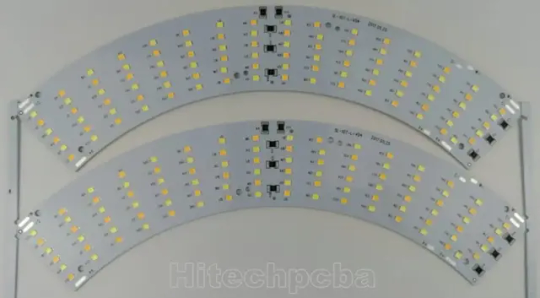
LED PCB Assembly
What is the LED Circuit Board assembly?
Generally, LED PCB assembly is considered to be a circuit board that has the LED components soldered to it. The LED is soldered to the printed circuit board and features a chip that creates the light as electrically connected. A thermal heat sink and a ceramic base are used to bond the chip. Not all the PCB products can be used in Led industry, as an LED PCB is easy to create a high volume of heat, but making it hard to cool with traditional methods. For this reason, metal core PCB is widely used in LED application because of their enhanced ability to dissipate heat, especially aluminum pcb is often used to fabricate PCB for LED lights.
We’ve had great LED PCB assembly experiences with top LED chips to brand such as Cree, Luxeon, Osram, Nichia, Lumileds, MLS, EVERLIGHT, Samsung, LG, Seoul., etc. PCB LED lights can be incorporated into numerous lighting applications due to their combination of excellent energy efficiency, low cost and maximum design flexibility.

Application of LED PCB Assembly
Hitechpcba serves customers in different industries, providing highly reliable and innovative LED PCBs for various applications:
• Horticulture light LED PCB Assembly
• LED controller PCB Assembly
• Computer LED display and indicators
• LED lights PCB Assembly for medical use
• Automotive LED PCBs Assembly include PCBs for brake lights and headlights
• Street lighting LED PCB Assembly
• Flashlights and camping accessories
• Traffic light PCB Assembly
• Commercial lighting LED PCB Assembly
LED PCB Assembly specification
Number of layers for LED PCB
These layers are made up of aluminum and magnesium, but now have Copper base material and Ceramic base materials for LED PCB industry, we can meet it.
Aluminum LED PCBs stand out among other PCBs because it has a good insulation characteristic and has a better machinery performance, the cheap cost is one important factor too.
Types of layers for LED PCB Assembly
Normally, the base layer is made using aluminum alloy metal.
This aluminum alloy substrate used in making the base makes it ideal for through-hole technology which transfers and dissipates heat.
A thermal insulation layer is made using some ceramic polymer which has good viscoelasticity characteristics.
It is highly heat resistant and protects the PCB against heat and mechanical stress.
The circuit layer, which is covered by a copper foil which can range from one to ten ounces.
LED Board type- single or in panel
Some boards are shapeless. For this reason, LED PCB panels are used. This reduces time, labor production and testing time.
Some LED PCB Assembly is done on a single board while others are done on panel boards.
LED PCB Assembly Process
Roughly, the PCBA process can be divided into theses phases: soldering paste printing > SMT (surface mounted technology) > reflow soldering > AOI (automated optical inspection)> THT (through-hole technology) > wave soldering > touch-up and cleaning > IC-programming > FCT (functional tests) > aging testing.
Below we show you the process.
Step1. Summarizing Project Information
Before contacting your supplier, make sure you have all the project information. Suppliers will need info following for quoting LED PCB assembly:
Gerber
BOM
LED PCB specification
Quotation quantity
Once you have gathered these information, you can contact us and request for a quote.
Of course, you can also provide the schematic, LED PCB Assembly pictures and even samples to us. The more details they have, the more accurate the supplier’s quotation will be.
Step2. Discussion and details about custom LED PCB Assembly
Different projects will have different requirements. Remember the special requirements mentioned in step 1? That’s going to be the focus of this session. Equipment and engineering capacity will not be identical between suppliers. Make sure your supplier has the equipment to produce and assemble major components and the corresponding testing capabilities.
For example, some vendors don��t have X-ray testing equipment, which means they can’t check the mount quality of BGA chips. Outsourcing this step will increase risk and cost. That’s what you don’t want.
Also, pay attention to time taken by the supplier to quote. Motherboards often contain hundreds or even thousands of components, and they are supplied by different manufacturers. To ensure the quality of the components, the supplier sourcing team will make multi-inquiries from these manufacturers or authorized suppliers to match customer’s requirement, which usually takes 2-3 business days, and even longer for some scarce chips. Therefore, if your project is complex and the supplier quotes you within few hours, double check with them.
Step3. Sample and feedback
After confirming the PI, the supplier will usually provide pre-production samples for your approval. At the same time, the supplier will also confirm with you the logistics plan of the bulk goods. Make sure they understand your shipping requirements, including details on packaging, customs clearance, taxes, etc.
For us to have a successful LED PCB Assembly process, its functions must be defined. Compliance requirement is defined to reduce the effect when components are selected.
The Bill of Materials is then generated from the information installed on the LED PCB.
All this information is used to assemble components which are identified from MOB to the LED PCB.
After that, the routing of traces is determined to each component, based on the size, shape of the circuit board and location of connectors.

Hitech Circuits is trusted by thousands of electronic engineers on their LED PCB assembly projects, from consumer, led bulb to precisely medical LED light, we can help you from the beginning of design stage; From commercial flood LED to industrial high power LED, from automotive LED to military LED, Venture is the perfect place for your LED PCB assembly requirement.
Hitech Circuits has been participated in hundreds and thousands of LED lighting projects, by providing LED PCB and also LED PCB assembly service.
Our LED PCB assembly had covered both ends of the Lighting Class LED size spectrum, assembling some of the largest (2 meter long boards) and some of the smallest LED Lighting applications which used in Medical Endoscopes.
LED PCB Assembly is very crucial in the current industrial development. Many electrical devises are being innovated and the old once being improved.
LED PCBs are useful due to the fact that they are made using materials that can transfer and dissipate heat. This characteristic increases device durability.
The world is changing with new technology, especially PCB technology that plays an essential role in the application of LED circuits. And the LED industry is taking advantage of this technology and growing faster.
As a full feature PCB solutions provider with more than a decade of experience, we're capable to provide LED PCB fabrication, components procurement and LED PCB assembly all under one roof. We can work with you to develop metal core PCB, aluminum circuit boards customized to your specific applications. We feature competitively priced PCBs made with standard FR-4 material that includes a thermal aluminum clad layer that will efficiently dissipate heat, keep all LED PCB components cool and significantly enhance the performance of your products.

LED pcb board, LED pcb assembly
LED with its advantages of high brightness, high efficiency, low heat, long life, is considered the most development potential in the 21st century lighting. In the market and policy driven by the rapid development of the domestic LED industry blowout has formed a relatively complete industrial chain, including the production of epitaxial wafers, chip preparation, packaging, integration, LED application. In 2010, China's LED industry scale, up from $ 827 billion in 2019 to 220 billion yuan, an annual growth rate of over 70%, higher than the 50% level of growth of the global LED lighting industry output value. Among them, the middle and lower reaches of the most complete industrial chain, accounting for 90% of the overall percentage of the GDP.Chinahas become the world's leading LED manufacturing base and important application market.
To further promote the technological innovation of the LED industry, construction and wide application of independent industry chain, China Electronic Appliance Corporation and industry associations to organize the theme of "Focus on the core energy LED Exhibition will be held November 9-11, 2010 in Shanghai International Expo Center and the 78th China Electronics Fair over the same period will be held will create from raw materials, epitaxial wafers, chip, LED bracket, LED accessories, LED packaging and supporting materials, the LED backlight upstream firm to the upstream and downstream enterprises of the display, lighting, landscaping, decorative lighting, traffic lights, automotive lighting, special lighting, to the equipment, instrumentation, software, finance, consulting and other service enterprises and technological exchanges and market trading platform, help the domestic industry sustained and healthy development, and promote the steady expansion of the LED application market.
In the LED industry chain upstream of the epitaxial wafers and LED chips accounted for 70% of the profits of the whole industry, and technology-intensive, capital-intensive, where the core technology of the LED. Well-known epitaxial wafer and chip production enterprises will be exhibited a number of energy-efficient, low heat, cost-effective LED products, many of whom have excellent products of international advanced level.
LED electronic pcb assembly manufacturing 100% Original LED Chip with one-stop in-house pcba services
3 notes
·
View notes
Text
Flex PCB Details Display......
#FPCway#flex PCB#flexible circuit board#rigid-flex PCB#Rigid-flex circuit board#FPC prototype#flex PCB and assembly#rigid-flex PCB manufacturer#flex PCB assembly#flex PCB and SMT#FPC manufacturer#flex circuit prototype#fpcway.com
0 notes
Text
What is PCB Assembly ?
PCB Assembly manufacturer - Hitech Circuits Co., Limited
It’s the step in the manufacturing process in which you populate a blank board with the electronic components needed to make it into a functional printed circuit board. It’s these components that make a board into the circuit that enables an electronic product to function. PCB assembly typically takes place via one of two processes:
1. Surface-mount technology
SMT: SMT stands for “Surface Mount Technology“. The SMT components are very small sizes and comes in various packages like 0201, 0402, 0603, 1608 packages for resistors and capacitors. Similarly for Integrated circuits ICs we have SOIC, TSSOP, QFP and BGA.
The SMT components assembly is very difficult for human hands and can be time taking process so it is mostly done by automated pick and place machine.
2. Through-hole manufacturing
THT: THT stands for “Through hole Technology”. The components with leads and wires, like resistors, capacitors, inductors, PDIP ICs, transformers, transistors, IGBTs, MOSFETS are example.
The component has to be inserted on one side of PCB and pulled by leg on other side and cut the leg and solder it. The THT components assembly is usually done by hand soldering and is relatively easy.
Printed Circuit Board Assembly Techniques
There are only two common PCBA techniques available for use by a PCB designer. The methods are:
1. Automated PCB Assembly Techniques
Generally, this technique employs the use of state of the art machines, which are fully automatic. For example, the surface mount components are worth positioning with the aid of an automated pick and place machine.
Again, reflow soldering is commonly for surface mount components usually done in a reflow oven. An automated solder stencil is also used to apply the solder paste on the PCB.
Finally, high tech inspection machines are used to confirm and check the quality of the PCBA. Some of which include: Automated optical inspection machine (AOI), X-ray inspection machines, etc.
Above all, due to the precise monitoring, control of soldering, no human input and versatile machines.
This technique ensures utmost efficiency, output consistencies, and limits defects.
2. Manual PCB Assembly Techniques
This method is favorite for use with through-hole parts, which needs manual placement on the board. Besides, with these through-hole parts, it’s advisable you use wave soldering. Note that in the through- hole assembly process, you need to place the components and electronics on the PCB.
After that, you use wave soldering to solder the leads. Typically, you will need an individual to insert a component into a marked PTH. Once done, transfer the PCB to the next station where the next person will be on standby tasked with fixing another part.
What are the Benefits of SMT PCB Assembly?
SMT assembly provides many benefits and some of them are as follows:
It can be used to incorporate small components.
In SMT, the components can be placed on both sides of the board.
It assures high component densities.
Fewer holes need to be drilled for surface mounting than through-hole.
It require low initial costs and time for setting up the mass production.
SMT is the simpler and faster-automated assembly when compared to through-hole.
Errors regarding the component placement can be easily rectified.
Surface mount PCBs feature strong joints, which can easily withstand vibrations.
What are the techniques used in Surface Mount Technology?
There are several techniques for the reflow process. After applying the solder paste or a flux mixture on the board and after placing the components, the boards are conveyed to a reflow soldering oven. The techniques used for reflowing soldering include infrared lamps, hot gas convection, fluorocarbon liquids with a high boiling point, and so on.
What are the different testing methods used in SMT PCB Assembly?
Hitech Circuits as the PCB assembly manufacturer, we perform the following testing and inspection to ensure the quality of surface mount PCBs.
Automated Optical Inspection (AOI): This is performed before and after the soldering to identify the component placement, presence, and solder quality.
X-ray Testing: In this type of testing, the operator relies on the X-ray images of the PCB to check the solder joints and lead-less components such as Quad Flat Packs and ball grid arrays, which are generally not visible to naked eyes.
In-Circuit Testing (ICT): This method is used to detect manufacturing defects by testing the electrical properties in the SMT Assembly.
What type of files or documents should I send for SMT PCB Assembly?
Gerber Files: The file contains all details of physical board layers including solder masks, copper layers, drill data, legends, and so on.
Bill of Materials (BOM): This contains information on the list of items needed for the PCB manufacturing and the instructions of manufacturing.
Pick and Place File: This file contains information on all components to be used in the PCB design and their rotation and X-Y coordinates.
The whole process of PCB Assembly
1. Bare board loader machine
The first step in the PCB assembly is to arrange the bare boards on the rack, and the machine will automatically send the boards one by one into the SMT assembly line.
2. Printing solder paste
When PCB on the SMT production line, firstly, we have to print solder paste on it, and the solder paste will be printed on the pads of the PCB. These solder pastes will be melt and solder the electronic parts to the circuit board when it passes through the high-temperature reflow oven.
In addition, when testing new products, some people will use film board/adhesive cardboard instead of solder paste, which can increase the efficiency for adjusting the SMT machines.
3. Solder paste inspection machine(SPI)
Since the quality of solder paste printing is related to the quality of welding of subsequent parts, some SMT factories will use optical machine to check the quality of solder paste after printed the solder paste in order to ensure stable quality. If there any poorly printed solder paste board, we will wash off the solder paste on it and reprint, or remove the excess solder paste if there is redundant solder paste on it.
4. High speed SMT machine
Usually, we will put some small electronic parts (such as small resistors, capacitors, and inductors) to be printed on the circuit board first, and these parts will be slightly stuck by the solder paste just printed on the circuit board, so even if the speed of printing is very fast and the parts on the board will not fall away. But large parts are not suitable for use in such high speed SMT machines, which will slow down the speed of small parts assembly. And the parts will be shifted from the original position due to the rapid movement of the board.
5. Universal SMT machine
Universal SMT machine is also known as "slow machine", it will be assembled some large electronic components, such as BGA IC, connectors, etc., these parts need more accurate positions, so the alignment is very important. Use a camera to take a picture to confirm the position of the parts, so the speed is much slower than High speed SMT machine we taked before. Due to the size of the components here, not all of them are packed in tape and reel, and some may be packed in trays or tubes. But if you want the SMT machine to recognize the trays or tube-shaped packaging materials, you must configure an additional machine.
Generally, traditional SMT machines are using the principle of suction to move electronic parts, and in order to place the parts successfully, and there must be the flat surface on these electronic components for the suction nozzle of the SMT machine to absorb. However, for some electronic parts don’t have a flat surface for these machines, and it is necessary to order special nozzles for these special-shaped parts, or add a flat tape on the parts, or wear a flat cap for thees electronic parts.
6. Manual parts or visual inspection
After assembled all parts by the high speed SMT machine or Universal SMT machine and before going through the high-temperature reflow oven, and we will set up a visual inspection station here and to pick out the deviation parts or missing components boards etc., because we have to use a soldering iron to repair if there are still defectives boards after passing the high-temperature oven, which will affect the quality of the product and will also increase the cost. in addition, for some larger electronic parts or traditional DIP parts or some special reasons cannot be processed by the SMT machine before, they will be manually placed on pcb here.
7. Reflow oven
The purpose of reflow oven is to melt the solder paste and form a non-metallic compound on the component feet and the circuit board, that means to solder electronic components on the circuit board. The temperature rise and fall curves often affect the soldering quality of the entire circuit board. According to the characteristics of the solder materials, usually the reflow oven will set the preheating zone, soaking zone, reflow zone, and cooling zone to achieve the best soldering effect.
For example, the melting point for SAC305 solder paste with lead-free is about 217°C, which means that the temperature of the reflow oven must be higher than the melting points to remelt the solder paste. What's more, the maximum temperature in the reflow furnace should not exceed 250°C, otherwise many parts will be deformed or melted because they cannot withstand such a high temperature.
Basically, after the pcb passed through the reflow oven, the assembly for the entire circuit board is almost complete. If there are hand-soldered parts, we need to transfer to DIP process, and then we have to check the quality after reflow oven by QC department.
8. Automatic optical inspection(AOI)
The main purpose of setting up AOI is because some high density boards can’t be process the following ICT test, so we used AOI inspection to replace it. But even using AOI inspections, there still have the blind spots for such checking, for example, the solder pads under the components cannot be checked by AOI. At present, it can only check whether the parts have side standing issue, missing parts, displacement, polarity direction, solder bridges, lack of soldering etc., but cannot checking the BGA solderability, resistance value, capacitance value, inductance value and other components quality, so far AOI inspection can’t completely replace ICT test.
Therefore, there is still some risk if only AOI inspection is used to replace ICT testing, but ICT test is also not 100% make sure the good quality, we suggest these two ways can be combined with together to make sure the good quality.
9. PCB unloader machine
After the board is fully assembled, it will be retracted to the unloder machine, which has been designed to allow the SMT machine to automatically pick and place the board without damaging the quality for PCB.
10. Visual inspection for finished products
Normally there will be a visual inspection area in our SMT production line whether there is an AOI station or not, and it will help to check if there are any defectives after completed assembled the pcbs. If there is an AOI station, it can reduce the visual inspection worker on our SMT line, and to reduce the potential cost, and because it is still necessary to check some places that cannot be judged by AOI, many SMT factories will provide the mainly visual inspection templates at this station, which is convenient for visual inspection worker to inspect some key parts and polarity for components.
11. DIP process
DIP process is a very important process in the whole PCBA processing, and the processing quality will directly affect the functional for PCBA boards, so it is necessary to pay more attention to the DIP process. There are many preliminary preparations for DIP process. The basic process is to re-process the electronic components first, like to cut the extra pins for some DIP components, our staff received the components according to the BOM list, and will check whether the material part numbers and specifications are correct or not, and performs pre-production pre-processing according to the PCBA samples. The steps are: Use various related equipment (automatic capacitor pins cutting machine, jumper bending machine, diode and triode automatic forming machine, automatic belt forming machine and other machines) for processing.

12. ICT test
Printed Circuit board open/short circuit test (ICT, In-Circuit Test), The purpose of ICT test is mainly to test whether the components and circuits on the printed circuit board are open or short issues. It can also measure the basic characteristics of most components, such as resistance, capacitance, and inductance values to judge whether the functions of these parts are damaged, wrong parts or missing parts etc. after passing through the high-temperature reflow oven.
ICT test machines are divided into advanced and basic machines. The basic ICT test machines are generally called MDA (Manufacturing Defect Analyzer). It’s just to measure the basic characteristics of electronic components and judge open and short circuits issue we talked above.
In addition to all the functions of the basic ICT test machines, for advanced ICT test machine can also test the whole PCBA by using power, start to testing the PCBA boards by setting the program in the test machine. The advantage is that it can simulate the function of the printed circuit board under the actual power-on condition, this test can partly replace the following functional test machine (Function Test). But the cost for the test fixture of this advanced ICT test can probably buy a car, it’s too expensive and we suggest it can be used in mass production products.
13. PCBA function test
Functional testing is to make up for the ICT test, because ICT only tests the open and short circuits on the the PCBA board, and other functions such as BGA and other fuctions are not tested, so it is necessary to use a functional testing machine to test all functions on the whole PCBA board.
14. Cutting board (assembly board de-panel)
Normally, printed circuit boards will be produced in panel, and it will be assembled to increase the efficiency of SMT production. It means several single boards in one panel, such as two-in-one, four-in-one etc. After finished all the pcb assembly process, it needs to be cut into single boards, and for some printed circuit boards with only single boards also need to cut off some redundant board edges.
There are several ways to cut the printed circuit board. You can design the V-cut using the blade cutting machine (Scoring) or directly manually break off the board (not recommended). For more high density circuit boards, it will be used the professional splitting machine or the router to split the board without any damage the electronic components and printed circuit boards, but the cost and working hours will be a little longer.
Why Choose Hitech Circuits PCB Assembly Manufacturer for Your PCB Assembly Projects?
There are several PCB manufacturers specializing in PCB assemblyservices. However, Hitech Circuits PCB Assembly stands out owing to the following:
Assistance in Material Procurement:
Technically, in PCB assembly services, the quality of parts is the responsibility of the OEM; however, we ease your job by assisting you to make the right selection. We can help you procure all your parts of the same type own a single part number, thanks to our supply chain and vendor network as well as experience. This saves time and cost that goes in ordering single parts as you plan.
Testing procedures:
We are very focused on quality and thus implement stringent testing procedures at each stage of the assembly and after completion.
Fast Turnaround Times:
Our well-equipped facility and the right tools enable us to complete your requirements well before time, and without compromising on the quality or functioning of the PCBs. For simple designs we revert in 24 to 48 hours.
Cost Effectiveness:
While PCB assembly is a cost-effective alternative, we go a step further and assure that the parts you list are of a good quality and suitable for your requirement. Also, you can control the part flow and replenish them as needed. This eliminates the need to buy extra stock and store it.
Quick Quote:
We offer a quick quote based on your BOM. All you need is a detailed BOM, Gerber files, your application requirement sheet, and quantity.
We’re not one to stand still, which is why we use the latest equipment and the finest minds to create your PCB projects. We’re constantly keeping our finger on the pulse of the latest trends. And as a result, we know how to deliver the highest standards of PCB assembly to meet all your requirements.
Our dedicated, friendly customer service team also means that we support you every step of the way. Offering our expert guidance to ensure a complete PCB project that you’re happy with.
Contact us today
No matter what your printed circuit board assemblyneeds are, we always aim to deliver efficient, dependable solutions. For more information about our services, do not hesitate to get in touch with us today for a no-obligation quote
2 notes
·
View notes