#Types of PCBs: PCBs come in different types
Explore tagged Tumblr posts
Visit Tumblr Blog
Explore Tumblr blogs with no restrictions, modern design and the best experience.
Last Seen Tumblr Blogs


Fun Fact
28.6 is the average number of monthly visits per US mobile user.
Text
The Benefits of Ordering Printed Circuit Boards Online: A Guide to Choosing the Right PCB Manufacturer
In today's rapidly advancing technological landscape, printed circuit boards (PCBs) play a crucial role in various electronic devices, from smartphones to industrial machinery. As demand for these essential components grows, businesses and hobbyists alike seek efficient and cost-effective solutions for obtaining high-quality PCBs. One of the most convenient methods is to order printed circuit boards online. In this article, we will explore the advantages of ordering PCBs online and provide insights into selecting a reputable PCB manufacturer.
Why Order Printed Circuit Boards Online?
Ordering printed circuit boards online offers several benefits, making it an attractive option for many businesses and individuals:
Convenience: The ability to order PCBs from the comfort of your home or office eliminates the need for in-person visits to manufacturers or suppliers. This convenience saves time and effort, allowing you to focus on your projects or business operations.
Wide Range of Options: Online PCB manufacturers offer a variety of options in terms of materials, layer counts, finishes, and more. This flexibility allows you to customize your PCBs according to your specific requirements and budget.
Cost-Effectiveness: Many online PCB manufacturers provide competitive pricing, especially for bulk orders. Additionally, you can easily compare prices and services from different providers, ensuring you get the best value for your money.
Quick Turnaround Times: Online ordering often comes with expedited production and shipping options, allowing you to receive your PCBs faster. This is particularly beneficial for projects with tight deadlines or when you need quick prototypes.
Access to Advanced Technologies: Many online PCB manufacturers offer advanced technologies such as high-frequency PCBs, flexible PCBs, and more. This access to cutting-edge technology ensures your designs are compatible with the latest industry standards.
Choosing the Right PCB Manufacturer
Selecting the right PCB manufacturer is crucial to ensuring the quality and reliability of your printed circuit boards. Here are some key factors to consider when choosing a PCB manufacturer:
Experience and Reputation: Look for a manufacturer with a solid track record and positive reviews from previous customers. Experienced manufacturers are more likely to produce high-quality PCBs and provide reliable service.
Quality Assurance: Ensure the manufacturer follows strict quality control measures, such as ISO certification and regular testing. High-quality PCBs are essential for the proper functioning and longevity of your electronic devices.
Customer Support: Good customer support is vital, especially if you encounter issues during the ordering process or with the final product. Choose a manufacturer that offers responsive and helpful customer service.
Manufacturing Capabilities: Check the manufacturer’s capabilities, including the types of PCBs they can produce, their layer count capacity, and the materials they use. Make sure they can meet your specific design requirements.
Lead Times and Shipping: Consider the manufacturer’s production lead times and shipping options. Quick turnaround times are crucial for meeting project deadlines, so choose a manufacturer that can deliver within your required timeframe.
Pricing and Payment Terms: While cost is an important factor, it should not be the sole consideration. Ensure the manufacturer offers transparent pricing and flexible payment terms that suit your budget.
Conclusion
Ordering printed circuit boards online is a convenient and cost-effective way to obtain high-quality PCBs for your projects. By choosing a reputable PCB manufacturer, you can ensure the reliability and performance of your electronic devices. Whether you are a business looking to streamline your supply chain or a hobbyist working on a personal project, ordering PCBs online provides a seamless and efficient solution.
For those ready to place a printed circuit board order online, consider the factors outlined above to select the right PCB manufacturer for your needs. With the right partner, you can bring your electronic designs to life with precision and quality.
#printed circuit board#pcb manufacturer#pcb supplier#printed circuit board order online#pcb design & manufacturing services#pcb circuit manufacturer in ahmedabad#electronic circuit design company
3 notes
·
View notes
Text
PCB Assembly Prototypes Manufacturer
PCB Assembly
What is a prototype PCB assembly?
PCB prototyping is the experimentation pilot stage of the product which is to be mass produced at a later stage. This is more of an experiment which is done after the initial discussions and the design. This offers a pre-production analysis of the boards that are to be manufactured, reducing the possible number of errors in the PCB design. PCB prototypes help the manufacturer analyze the strengths as well as weak areas of their proposed circuit boards. Prototypes also serve as a reference point for future versions of the same product. At Hitechpcba, we handle PCB prototype assembly in quantities from one to hundred printed circuit boards.
We have acquired capabilities that enable us to serve our clients better. All these years, we have worked on many complex prototype PCB assembly projects, and we believe the following capabilities have helped us serve our clients better.
Prototype PCB Assembly Services: We specialize in the following prototype printed circuit board assembly services.
SMT: We can provide single-sided and double-sided surface mount PCB assemblies in different specifications.
Plated Through Hole: We offer plated through hole assembly with selective soldering.
Mixed Assemblies: We often work on projects involving mixed assemblies – through-hole and SMT and electromechanical assemblies.
PCBA Testing: All the PCBA functional testing is performed in-house. Over the years, we have invested in various test fixtures and equipment, which helps us ensure the quality of PCBA. Currently, we provide the following types of PCBA testing services:
Flying probe testing for PCB
Functional testing including system and board-level testing
General PCB Assembly Capabilities: Our general PCB assembly capabilities are not limited to these:
RoHS, leaded or lead free, clean and no chemistries
PCB components including various types of QFNs, BGAs, 0105, 0201, 0804, and press fit components in small quantities.

What are the benefits of a prototype PCB assembly?
Prototype PCB assembly comes with several advantages. These benefits play a major role in the facilitation of your PCB manufacturing. Some of these benefits include:
Detection of Flaws Early
With prototype PCB, you will easily detect whatever flaws are present during the product’s development stages. This will allow you to solve the issues thereby saving you some money if you had gone ahead to make the production having the flaws in them.
If you go ahead to make changes during the production, there may be a need for more technicalities, and this may be expensive.
Testing of Each Component
With a prototype, you will be able to test all your system’s elements individually before you go ahead to set it up. You should do this because it is important especially for very complex projects composed of several parts that are PCB based.
When you validate each of these components, you will be able to identify those areas having issues that you should look into. This is the only way the project can function the right way.
Reduction in Total Costs
Utilizing the prototype bare PCB for any of your projects could go a long way in reducing what you’ll have spent in total for the project. With prototyping, you will be able to notice those errors in your project and then make corrections before you start the real production.
As soon as these flaws have been checked and rectified, then you may continue with the manufacturing of your Printed circuit boards in large quantities, thereby saving you unnecessary costs.

High-Quality PCBs
Why prototyping your PCB is important is to help you test if your project will function effectively. When we talk of testing, it involves the identification of errors present and then rectifying and making corrections to them.
Therefore, the eventual PCB after the prototyping will be of high quality that surely meets standards set internationally.
Less Turnaround Time
With prototype PCB assembly, you will be able to reduce the total time used in producing your printed circuit board. While making use of prototype printed circuit boards, you’ll be able to see the errors and then make corrections before you start the actual production.
Therefore, the eventual prototype will be free of defects. This implies that your PCBs will be produced quickly by your manufacturer.
We are here :https://www.hitechpcba.com/pcb-assembly-manufacturer
6 notes
·
View notes
Text
Ultimate Guide to PCB Testing Methods: Ensuring Quality and Reliability in Your Circuits
In the electronics sector, Printed Circuit Boards (PCBs) are the life-lines of virtually all gadgets that are in use in the modern society. From humble home appliances to gigantic industrial equipment, PCBs are the skeletal framework of hardware organization and connection of circuit elements. It is vital to guarantee the quality and dependability of these fundamental parts – thus enters PCB testing methods. It is our hope that this extensive hand will help identify the most suitable test strategies for PCB testing, why these techniques matter, and how to maximize your circuits’ functionality.
Introduction

Firstly, an increase in the capability of different electronic devices leads to higher necessary requirements to the PCBs used in their production. Performing tests on the PCBs is an essential step in the manufacturing process done to confirm that a given board performs as a unit to the expected levels. This guide aims at explaining various techniques of PCB testing with a view of having a better understanding on how to achieve quality and reliability on the circuits.
Why PCB Testing is Crucial

PCB Testing When it comes to the potential defects on PCBs, there are shorts, opens, and some component placements. They can cause device failure, decline in performance level, and sometimes also pose safety issues. Through high-quality testing regimes, it becomes easier to address problems before they reach the customer, and thus manufacturers will have reliable and efficient products. Key reasons for PCB testing include:
Detecting Manufacturing Defects: Solder bridges, missing and placed in wrong position components, all can be detected in the initial stages easily.
Ensuring Functionality: Ensuring that the PCB does what is wanted and needed when it is in use, and under several conditions.
Quality Assurance: Ensuring that the business meets industry standards, and what clients require of them.
Cost Efficiency: Decreasing the likelihood of rework and recall by identifying possible defects before they get to the customer.
Types of PCB Testing Methods
These are the types of PCB Testing Methods:
Visual Inspection

Technique one as also referred to as the VI or visual inspection is the simplest and basic type of testing done on PCBs. The technique entails inspecting the board with naked eyes for some of the common faults including solder bridges, missing parts, and misalignment issues.
Automated Optical Inspection (AOI)

AOI employs cameras and software algorithms to check PCBs for defects and performs the inspections singly. This method of inspection is far more efficient than the manual inspection and simultaneously versatile enough to identify numerous problems.
X-ray Inspection

Some functions which include examination of features of BPCs that could not be easily inspected include solder joints under components through x-ray inspection. It is especially effective in inspecting defects in BGA (Ball Grid Array) and other various packages as well.
In-Circuit Testing (ICT)
ICT entails applying different voltage across the PCB to checks on the electrical characteristics of the needy part and connections. The use of this method is highly recommended for the identification of functional problems and verification of the circuit’s goodness.
Functional Testing (FCT)
Functional testing evaluates the effectiveness of the PCB pointing to the fact that it can be tested when placed in use. This method enables the certification of that the PCB works as expected under actual environment.
Flying Probe Testing
In flying probe testing, the probes are moved around to test the electrical properties of the created PCB. Lower to medium volume production runs can be made easily by using this technique; hence it is advantageous in this regard.
Boundary Scan Testing
Boundary scan testing also called as JTAG testing extends test circuitry into all the components for testing the connections between them. Although, this method is very efficient for identifying connection problems and faults.
Burn-In Testing
Burn-in testing puts the PCB in a state of operational stress for a long time to capture early-life failures. This aspect makes the method reliable for the long term since it is likely to identify problems that may occur when the equipment is in use for a long time.
Detailed Analysis of Each Testing Method works
These are the detailed analysis of each testing method works:
Visual Inspection
Pros:
Simple and low-cost
Determined to be a system for the reporting of noticeable defects as soon as they are observed.
Cons:
Time-consuming for complex boards
Limited to visible defects
Automated Optical Inspection (AOI)
Pros:
Fast and accurate
Is capable of detecting various kinds of defects.
Non-destructive
Cons:
High initial setup cost
May need to have better settings optimized for specific boards.
X-ray Inspection
Pros:
Examines hidden features
Ideal for complex packages
Cons:
Expensive equipment
Requires skilled operators
In-Circuit Testing (ICT)
Pros:
Thorough electrical testing
High fault coverage
Cons:
Requires custom fixtures
Not for all the boards or servers that you wish to build.
Functional Testing (FCT)
Pros:
Ensures real-world performance
Detects system-level issues
Cons:
Time-consuming
The mathematical test object can involve complex arrangements of test configurations.
Flying Probe Testing
Pros:
Flexible and adaptable
Cost-effective for small batches
Cons:
Slower than ICT for big volumes
Applicable only when the board is specially designed
Boundary Scan Testing
Pros:
Interconnections have high fault coverage.
Said; No need to have physical access to the test points
Cons:
Requires boundary scan-enabled components
Complex setup
Burn-In Testing
Pros:
Identifies early-life failures
Ensures long-term reliability
Cons:
Time-consuming and costly
Perhaps stressful to the board
Choosing the Right Testing Method
The choice of the appropriate method of PCB testing can be influenced by several factors such as the level of complexity of the PCB and the numbers of boards to be tested as well as the actual costs of the testing process and other features. Consider the following when choosing a testing method:
Board Complexity: Great board densities or component placement can be a determinant as to whether one needs AOI or X-ray inspection.
Production Volume: Applications that are characterized by high volumes can be easily facilitated by ICT while the low to medium volume applications may require flying probe testing.
Budget: Both manual inspection and AOI are favorable for various production volumes, while X-ray and ICT are more expensive at the beginning.
Specific Requirements: There are two types of the test, namely Functional Test and Burn-In Test that should be made so as to attain the long term reliability in applications that are critical.
Best Practices for PCB Testing
Using the best techniques in testing PCBs increases the quality and reliability of the circuits that you are working on. Here are some key practices to follow:
Early Testing: It is recommended to carry out the tests when the product is still in its design and manufacturing phase so that problems can be noted earlier before they reach a very catastrophic level.
Automate Where Possible: Use method such as automation to reduce the time and improve on the quality of the testing.
Regular Calibration: It is necessary to check if all the testing equipment used for calibration are accurate.
Comprehensive Coverage: This way, you will be able to ensure that there are no defects that are not tested as the best testing approach combines all types of testing methods.
Document Everything: Ensure that you keep records of the tests performed, the results obtained, as well as any measures taken to correct the breaches.
Common Challenges and How to Overcome Them
These are the common challenges and how to overcome them:
False Positives/Negatives
Automated testing methods maybe good some times, they give you the results that are either positive or negative and this will lead to unnecessary rework or more alarming leaving critical defects unfound. In order to avoid this, make sure that testing algorithms and testing equipment are updated and fine-tuned from time to time.
Component Access
Some of the testing techniques involve handling parts of the circuit and with high density board this can be very difficult. Some of the ways in which testbench implementation can be avoided are as follows Boundary scan testing and X-ray inspection.
High Costs
Some form of testing such as X-ray and ICT testing is often very costly. The effectiveness must come with reasonable prices; try to combine some of the mentioned approaches to cover all the aspects without spending too much money.
Future Trends in PCB Testing
About the future, it can be stated that its trends will be in fact linked to the tendencies in technologies and expectations towards ever higher quality and quantity of tested PCBs. Key trends to watch include:
AI and Machine Learning: Using of intelligence algorithms and machine learning in testing algorithms to enhance the efficiency and the minimization of false negative or false positives.
IoT and Smart Manufacturing: Higher testing flexibility and opportunities for the continuous test process supervision.
Advanced Imaging Techniques: The need for better techniques that would enhance the detection of defects within a printed circuit.
Environmental Stress Testing: More focus in the testing of PCBs under different environmental pressures in order to improve on its longevity.
Conclusion
Quality and reliability of packaged circuits have to be maintained to contribute positively in any electronic equipment. This paper seeks to explain the common testing techniques for PCB so that PCB manufacturers are able to test and see if they are free from defects and if they are functional. This ultimate guide will give you a full insight on the available options in PCB testing that will enable you make the best decision that will give you perfect circuits.
The aim is to help you understand how to attain the best quality of PCBs, what methods are worth following, and what trends drive future improvements, thus contributing to the quality of the final electronic products and, consequently, consumer satisfaction.
#PCBTesting#Electronics#CircuitBoard#QualityControl#Engineering#Technology#Manufacturing#IndustrialDesign#Tech#Innovation
2 notes
·
View notes
Text
its that time again! my touhou posting continues. this is the most important one though, so you definitely wanna read this one. trust me :P
nina's thoughts on Touhou 8 - Imperishable Night
Imperishable Night is the best game ever made it has Wriggle Nightbug in it and she's the coolest touhou so this game is the bestest of all of them 100% perfect game!!!
jk. kinda.
Imperishable Night takes a big step forward in a lot of places, expanding on what worked well in PCB and making changes to what didn't, with a handful of really cool features unique to this game.
for starters, the playable character roster has exploded from three characters to EIGHT characters, split into four teams of two each with a human and a youkai. unfortunately none of the teams have any alternate movesets so theres technically only 4 choices, but the characters in each pair have different enough shots that you basically have 8 different weapon types to utilize. Reimu returns partnered with Yukari, Marisa is joined by Alice, Sakuya is back again with her mistress Remilia, and Youmu and Yuyuko join in as a duo of newbies. i tried out all four pairs and cleared stage 6A with each (although i admit to using continues for most of those runs) but MariAli was my fav so i went with them to get the true clear with a 1cc-6B. i love how theres a technique for Marisa and Alice where you can make use of Alice's laser taking a half second to disappear and instantly reappearing on swap, swapping with a good rhythm to keep full uptime on Alice's laser while also shooting out bullets as Marisa to get really high damage output. not only is it a fun maneuver to pull off, but it has an amazing name given by the fandom: the MALICE BEAM!
on the topic of swapping, what you do when playing as either human or youkai affects certain mechanics in IN, most notably the Time system. when you first start a run off IN the time starts at 11pm and if you reach 5am your run ends. using a continue takes a half hour, and clearing a stage typically takes an hour off of your total, but you can make a stage only take half an hour instead if you collect enough time points. the main source of time points comes from the human/youkai meter. when you do things as your human or youkai partner the meter moves in their respective direction; when its maxed on humanity you gain time points through shooting enemies, and when its maxed on youkai-ness you gain time points for grazing bullets. a couple other mechanics also work based on your human/youkai status, like enemy summons that dont damage youkai but also can't be hurt by their bullets. the time system is a bit tough to understand, but its theoretically optional since if you 1cc you won't really run out of time anyways, and it allows for wiggle room later in runs if you managed to clear earlier stages within the half-hour, and the game doesn't punish you with a bad end for continuing like others do.
for new characaters, all i have to say is WRIGGLE NIGHTBUG!! LETS GO BABY!! WRIGGLE SWEEP!!!! Wriggle is probably my fav character in touhou just in general, let alone from this game. is she just a first stage boss with very little to do? yes. does she basically never show up again outside this game? also yes. do i care? no! Wriggle is an adorable firefly lady and the self-titled queen of insects, she can talk to and command bugs to do her bidding, and she frequently hangs out with other characters i like such as Rumia and Cirno and the next character i talk about from this game. this is absolutely a biased take because i love bugs but i dont care, Wriggle is the best. (plus shes totally trans-coded, definitely not me projecting :P) Nightbug aside, the other characters in IN are pretty solid too! Mystia is great, although that one is also probably a bit biased because her izakaya fangame is incredibly good and does a great job endearing you to her. gotta respect the grind of a bird youkai opening a fried food stand but selling eels instead of the expected chicken cause she doesn't wanna feed birds to people. also the fact that she scams people by afflicting them with night-blindness without their knowledge and then selling her fried eels as a cure is so funny. Mokou is an all around solid character, i love the concept of this immortal phoenix lady who hates the immortal moon princess so much, and neither one can die so they just beat the shit out of each other all the time (and maybe kiss? classic enemies to lovers) and her design is really sick, the detail of having a bunch of fire-warding charms plastered all over so she doesn't light her outfit on fire is hilarious lol.
does Imperishable Night have flaws? yeah for sure. needing to unlock stage 6b is kinda lame, and stuff like the last spells are weird mechanics that don't really do anything. however, WRIGGLE NIGHTBUG IS IN THE GAME LETS GO BABY WRIGGLE NIGHTBUG BEST TOUHOU EVER WOOOOOOOOOOO-

8 notes
·
View notes
Text
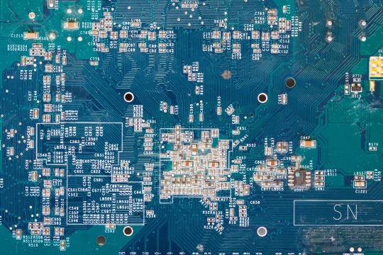
Circuit Board, PCB assembly & electronics manufacturing service provider from China (hitechcircuits.com)
What is a prototype PCB assembly?
PCB prototyping is the experimentation pilot stage of the product which is to be mass produced at a later stage. This is more of an experiment which is done after the initial discussions and the design. This offers a pre-production analysis of the boards that are to be manufactured, reducing the possible number of errors in the PCB design. PCB prototypes help the manufacturer analyze the strengths as well as weak areas of their proposed circuit boards. Prototypes also serve as a reference point for future versions of the same product. At Hitechpcba, we handle PCB prototype assembly in quantities from one to hundred printed circuit boards.
We have acquired capabilities that enable us to serve our clients better. All these years, we have worked on many complex prototype PCB assembly projects, and we believe the following capabilities have helped us serve our clients better.
Prototype PCB Assembly Services: We specialize in the following prototype printed circuit board assembly services.
SMT: We can provide single-sided and double-sided surface mount PCB assemblies in different specifications.
Plated Through Hole: We offer plated through hole assembly with selective soldering.
Mixed Assemblies: We often work on projects involving mixed assemblies – through-hole and SMT and electromechanical assemblies.
PCBA Testing: All the PCBA functional testing is performed in-house. Over the years, we have invested in various test fixtures and equipment, which helps us ensure the quality of PCBA. Currently, we provide the following types of PCBA testing services:
Flying probe testing for PCB
Functional testing including system and board-level testing
General PCB Assembly Capabilities: Our general PCB assembly capabilities are not limited to these:
RoHS, leaded or lead free, clean and no chemistries
PCB components including various types of QFNs, BGAs, 0105, 0201, 0804, and press fit components in small quantities.

What are the benefits of a prototype PCB assembly?
Prototype PCB assembly comes with several advantages. These benefits play a major role in the facilitation of your PCB manufacturing. Some of these benefits include:
Detection of Flaws Early
With prototype PCB, you will easily detect whatever flaws are present during the product’s development stages. This will allow you to solve the issues thereby saving you some money if you had gone ahead to make the production having the flaws in them.
If you go ahead to make changes during the production, there may be a need for more technicalities, and this may be expensive.
Testing of Each Component
With a prototype, you will be able to test all your system’s elements individually before you go ahead to set it up. You should do this because it is important especially for very complex projects composed of several parts that are PCB based.
When you validate each of these components, you will be able to identify those areas having issues that you should look into. This is the only way the project can function the right way.
Reduction in Total Costs
Utilizing the prototype bare PCB for any of your projects could go a long way in reducing what you’ll have spent in total for the project. With prototyping, you will be able to notice those errors in your project and then make corrections before you start the real production.
As soon as these flaws have been checked and rectified, then you may continue with the manufacturing of your Printed circuit boards in large quantities, thereby saving you unnecessary costs.
High-Quality PCBs
Why prototyping your PCB is important is to help you test if your project will function effectively. When we talk of testing, it involves the identification of errors present and then rectifying and making corrections to them.
Therefore, the eventual PCB after the prototyping will be of high quality that surely meets standards set internationally.
Less Turnaround Time
With prototype PCB assembly, you will be able to reduce the total time used in producing your printed circuit board. While making use of prototype printed circuit boards, you’ll be able to see the errors and then make corrections before you start the actual production.
Therefore, the eventual prototype will be free of defects. This implies that your PCBs will be produced quickly by your manufacturer.

What are the different types of prototype PCB assembly services you offer?
With years of market presence and experience, we specializes in the following prototype PCB assembly services.
Plated through-hole (PTH): We can provide the through-hole assembly with selective soldering.
Surface mount technology (SMT): We offer single-sided as well as double-sided SMT board assemblies in varied specifications.
Mixed Assemblies: Our experts often work on projects involving both PTH and SMT assemblies.
What are the types of testing Hitechpcba use for prototype PCB assembly?
Automated Optical Inspection (AOI): This is performed before and after the soldering to identify the component placement, presence, and solder quality.
X-ray Testing: In this type of testing, the operator relies on the X-ray images of the PCB to check the solder joints and lead-less components such as Quad Flat Packs and ball grid arrays, which are generally not visible to naked eyes.
In-Circuit Testing (ICT): This method is used to detect manufacturing defects by testing the electrical properties in the SMT Assembly.
These techniques help us ensure the reliability and accuracy of the circuit boards. In addition to this, it ensures a long operational life of equipment, minimal production losses, streamlined processes, and much more.
What are the capabilities Hitechpcba offer for prototype PCB assemblies?
We specialize in offering IPC compliant, and quick turn PCB assemblies. We are very particular about our scheduled deliveries and timelines, and we deliver without compromising the quality. Our PCBA capabilities are not limited to these. Here are some capabilities we offer through prototype PCB assemblies.
RoHS compliance
Stringent testing procedures
Device encapsulation
Full turnkey, partial turnkey, and kitted/consigned services
Assemblies using Surface Mount (SMT), Thru-hole, Mixed Technology (SMT/Thru-hole), Single and double-sided SMT/PTH, Large parts on both sides, BGA on both sides.
Do you perform a component analysis for prototype PCB assemblies?
Yes, we check the quality and performance of components before mounting them on the circuit boards. This is because a malfunctioning component can affect the performance of the entire circuit board assembly and also pose risks.
What is your standard turnaround time for a prototype PCB assembly?
Our turnaround time for standard applications is two weeks. This timeframe varies depending on the complexity of the applications. However, we are committed to offering quick turnaround times without compromising on quality, functionality, and accuracy, which offers our client a competitive advantage and reduced time to market. You can also request any emergency assistance or queries related to any type of PCB assembly. Our experts will assist you in all possible ways.
How is the cost of prototype PCB assembly estimated?
PCBA costing varies based on the different factors, such as PCBA parts, type of materials to be used, order quantity, and much more. We can also offer quotes and customization options once you share the detailed requirement with us.
We focus on quality and customer satisfaction over anything else. This has helped us build a long list of happy and satisfied customers. So, if you wish to partner with a manufacturer of prototype PCB assembly in China, then don’t hesitate to reach us. Our experts will assist you through all the phases of the prototype PCB assembly process. We look forward to making your experience with us better and memorable.
How to choose prototype pcb assembly manufacturer?
Our pcb prototype assembly service includes the sourcing of components. This allows you to concentrate on what you do best: layout design. We have a dedicated sourcing staff that coordinates with multiple suppliers and distributors to purchase electronic parts as per client requirements, and our staff completes these purchasing particulars in a most efficient manner. We have advanced processes for optimal selection of packaging (cut tape, tube, bulk, etc.) to reduce the total cost. Furthermore, we are capable of cross-referencing parts and even locating hard-to-find and obsolete parts. Customers can be rest assured that when Hitech Circuits substitutes components that they are high quality: we only use the electronic component numbers and manufacturers specified in the BOM. We will not modify your original layout design. Part substitutions take place only with your permission.
The final pcb prototype assembly service cost includes assembly labor charges, bare circuit board rates, and part costs. We understand the importance of prompt delivery. The sooner the components are sourced, the sooner we can begin circuit board fabrication. We thoroughly evaluate engineering inquiries and concerns related to the related parts with our clients before commencing circuit board assembly. The average time taken for pcb manufacturing assembly is about two weeks, which can be further reduced if there are no hard-to-locate components or documentation mistakes.
We have specialized experts to deliver fast turnarounds for prototype circuit board assembly with surface-mount (SMT), through-hole (THT) and mixed-technology components.
Anyone interested in electronics and electronic circuit boards needs to understand the various stages of developing and producing a printed circuit board. It can come in handy when you are seeking a top prototype smt assembly provider. The various production stages of printed circuit boards entail design, prototyping (prototype PCB development and rapid prototyping pcb assembly), and PCB high volume production. Different entities will always seek part of the whole production process depending on their electronic circuit board needs.
However, this article seeks to help you understand everything about prototype PCB assembly, a fundamental aspect of the PCB production process.
Rapid prototyping pcb assembly represents a fundamental phase of the printed circuit production process. It is also inferred as PCBA prototype assembly, SMT or surface-mount technology PCB prototype, PCB sample assembly, etc. From these alternative names, the meaning of prototype assembly regarding printed circuit boards becomes apparent. So what is assembly prototype?
PCB prototype assembly service is a fast prototype printed circuit board assembly primarily used to test fresh or new electronic designs. Consequently, it assists with checking and ensuring quality assurance of the PCB. For instance, it verifies that no bug exists in the test PCB, updates the design, and finds bugs. In most instances, prototype assembly of an electronic project will require two or three iterations to ensure everything is perfect.

Why Choose Hitech Circuits PCB Assembly for Your Prototype PCB Assembly Projects?
There are several PCB manufacturers specializing in prototype PCB assembly services. However, Hitech Circuits stands out owing to the following:
1.Strong Supply Chain: Over the years, we have built strong supply chain relationships in the industry, which helps us fulfill the requirements of turnkey prototype assembly services easily.
2.Fastest Turnaround Times: Our engineering expertise coupled with our understanding of industry requirements and a well-equipped facility enables us to assure the fastest turnaround times of 24-48 hours.
3.Reliability: All the printed circuit boards that we produce are IPC compliant, which helps us assure reliability.
4.Competitive Pricing and Quick Quote: Our supply chain relationships enable us to assure competitive prices. The cost of the PCB prototype assembly will be made available within 24-48 hours.
2 notes
·
View notes
Text
Automated Test Equipment (ATE): What It Is and Why It Matters
Modern electronics and software systems require precise, fast, and scalable testing processes. That’s where automated test equipment (ATE) comes in. ATE plays a critical role in manufacturing, validating, and maintaining electronic components and systems with minimal manual intervention.
In this article, we explore automated test equipment—what it is, how it works, common types, key benefits, and its role in today’s software and hardware testing environments.
What is Automated Test Equipment (ATE)?
Automated Test Equipment (ATE) is a machine that automatically tests devices for functionality, performance, or defects. It is commonly used in electronics manufacturing and software testing to ensure that products meet required specifications before being shipped.
ATE systems are programmable and can simulate multiple test scenarios, record results, and quickly identify faults.
Key Components of ATE
Test Controller: The brain of the system, typically a computer running specialized software.
Test Interface: Hardware used to connect the ATE system to the device under test (DUT).
Instruments: Oscilloscopes, signal generators, multimeters, etc., used to perform measurements.
Software: Scripts and test sequences that define what and how tests are run.
How ATE Works
The device under test (DUT) is connected to the ATE system.
The ATE software executes a predefined test sequence.
Instruments measure voltage, current, response time, and other parameters.
The system compares actual results with expected outcomes.
A pass/fail report is generated.
This process is fully automated and can be repeated for hundreds or thousands of units with consistent accuracy.
Applications of ATE
Semiconductor Testing: Ensures microchips function correctly before packaging.
PCB Testing: Validates solder joints, circuit paths, and component integrity.
Consumer Electronics: Phones, TVs, wearables are tested in the factory using ATE.
Automotive Systems: Safety-critical systems like ECUs are tested for reliability.
Software/API Testing: Automated testing platforms like Keploy help simulate and validate backend systems and microservices.
Benefits of Automated Test Equipment
1. Speed and Efficiency
ATE systems test products far faster than manual testing, boosting production line efficiency.
2. Consistency
Automated systems reduce human error and ensure every unit is tested under the same conditions.
3. Scalability
Perfect for mass production—test hundreds of units per hour without increasing staffing.
4. Data Logging and Analytics
ATE software records data for quality control, trend analysis, and root-cause diagnostics.
5. Reduced Labor Costs
Once configured, ATE systems need minimal supervision.
Types of ATE
Type
Description
Semiconductor ATE
Tests integrated circuits, chips, and SoCs
PCB ATE
Used in circuit board assembly lines
Functional ATE
Tests a device's full functionality as a black box
Optical Inspection Systems
Uses cameras and sensors for visual defect detection
API / Software Testing Tools
Tools like Keploy automate API validation
ATE in Software Testing
While traditionally associated with electronics, the concept of ATE has been extended to software systems. Tools like Keploy serve as automated testing platforms for APIs, enabling test case generation, mocking, and regression testing based on real traffic.
Keploy automates the validation of REST APIs and microservices by:
Capturing real user traffic
Generating test cases and mocks
Running automated validations in CI/CD pipelines
Challenges of Using ATE
Initial setup cost can be high, especially for custom solutions
Requires specialized expertise to develop and maintain
May need updates as products evolve (especially in agile environments)
Hardware-specific tools might not scale well across different platforms
Future of Automated Testing
With advancements in AI and machine learning, future ATE systems will:
Predict potential failure points
Adapt dynamically to changing conditions
Integrate seamlessly with digital twins and Industry 4.0 initiatives
Combine hardware and software validation into unified platforms
Final Thoughts
Automated test equipment is a game-changer for ensuring quality, reducing errors, and scaling testing in both hardware and software environments. Whether you’re testing semiconductors or APIs, automation boosts efficiency and reduces costs. For software engineers looking to bring ATE principles to API testing, tools like Keploy offer smart test case generation and validation without manual effort—perfect for modern DevOps workflows.
0 notes
Text
What Are DIL Sockets and Why Are They Essential for Reliable IC Mounting?

Introduction: Why Do DIL Sockets Matter in Modern Electronics?
Dual In-Line (DIL) sockets, also known as DIP sockets, are foundational components in electronic design and manufacturing. These ingenious devices enable integrated circuits (ICs) to be easily mounted and replaced without requiring direct soldering to the board. Whether you're prototyping, repairing, or developing scalable designs, DIL sockets deliver unmatched flexibility, reliability, and protection. Their significance has only grown with the increasing complexity and miniaturization of circuits, offering a practical bridge between reusable hardware and robust design.
What Is a DIL Socket and How Does It Work?
A DIL socket is a mechanical connector with two parallel rows of contact pins designed to accommodate Dual In-Line Package (DIP) ICs. These sockets are mounted on printed circuit boards (PCBs) and serve as a host into which the ICs can be inserted or removed without risk of thermal damage or physical stress.
DIL sockets feature:
Two parallel rows of holes matching the DIP IC layout
Plated contact points to ensure stable electrical connections
Molded plastic bodies that resist heat and mechanical stress
Options ranging from 6 to 64 pins (and beyond) for various IC types
Their role is simple but powerful: make IC installation secure, reversible, and low-maintenance.
Why Choose DIL Sockets for Your PCB Projects?
When building or repairing PCBs, soldering directly onto the board is not always the best approach. DIL sockets offer several advantages that streamline your electronic assembly processes while safeguarding your components.
Key reasons to use DIL sockets:
Component Protection: Prevents heat damage during soldering by keeping ICs away from the soldering process.
Easy Maintenance: ICs can be swapped out or upgraded without desoldering, making repairs and modifications quick.
Cost-Effective Prototyping: Ideal for testing multiple ICs during development phases without damaging the board.
Reduced Wear on PCBs: Repeated IC replacement does not degrade the board’s pad or trace integrity.
ESD Isolation: Some DIL sockets come with built-in static protection features, helping shield sensitive ICs from electrostatic discharge.
What Types of DIL Sockets Are Available?
There’s no one-size-fits-all approach when it comes to DIL sockets. Several variants cater to different application needs—from basic home electronics to high-end embedded systems.
Common types of DIL sockets:
Turned Pin (Machined Pin) Sockets: High-quality, durable sockets with precision-machined contacts offering superior connectivity and long lifespan.
Stamped Pin Sockets: Economical options with stamped metal contacts, best for low-cost and temporary applications.
Open-Frame Sockets: Lightweight design ideal for space-sensitive applications.
Closed-Frame Sockets: Provide extra protection and rigidity, suitable for rugged environments.
Low-Profile Sockets: Reduce stack height, making them perfect for compact devices or portable electronics.
These variations help engineers select the right balance between cost, space, durability, and performance.
How to Select the Right DIL Socket for Your Project?
Choosing the appropriate DIL socket is vital to ensure the functionality and longevity of your circuit. Several factors must be considered based on your specific application.
What to look for:
Pin Count Compatibility: Match the socket’s pin count with the IC’s configuration (e.g., 8, 14, 16, 40 pins).
Pitch Size: Ensure the pitch (distance between pins) aligns with your PCB layout, usually 2.54mm for standard DIPs.
Contact Material: For better conductivity and resistance to oxidation, choose gold- or tin-plated contacts.
Operating Temperature Range: Match with your environmental conditions, especially for industrial or outdoor use.
Insertion Force: Low-force sockets reduce stress on IC pins, enhancing overall reliability.
Matching these specifications ensures smooth integration and long-term performance.
What Are the Typical Applications of DIL Sockets?
DIL sockets are found across numerous electronic applications—from hobbyist kits to mission-critical systems. Their versatility makes them an essential tool for anyone working with ICs.
Popular use cases:
Prototype Development: Ideal for temporary mounting of ICs during breadboarding or iterative testing.
Consumer Electronics: Used in TVs, DVD players, audio systems, and gaming consoles for easily replaceable logic circuits.
Educational Kits: Facilitates reusable learning tools for electronics students and hobbyists.
Industrial Control Systems: Enables fast field servicing of ICs in automation and monitoring equipment.
Retro Computing & Repairs: Crucial in repairing or upgrading vintage computers and devices using DIP ICs.
Microcontroller Boards: Commonly found in Arduino-compatible boards and DIY microcontroller projects.
Their plug-and-play nature simplifies design, reduces downtime, and enhances hardware sustainability.
Why Are DIL Sockets Still Relevant in an SMT-Dominated World?
Despite the rise of surface-mount technology (SMT), DIL sockets hold their ground in many modern applications. SMT may dominate mass production due to space-saving advantages, but for design flexibility, prototyping, and component longevity, DIL sockets remain unmatched.
Continued relevance stems from:
Tool-Free IC Swapping: No need for reflow ovens or hot-air rework stations.
Backward Compatibility: Supports legacy systems using DIP ICs.
DIY and Low-Volume Manufacturing: Enables small-scale developers to iterate designs affordably.
Field-Serviceability: Perfect for environments where rapid IC replacement is crucial.
In fact, many engineers intentionally design with DIP ICs and sockets to retain modularity and user-serviceability.
Conclusion: Are DIL Sockets the Unsung Heroes of PCB Design?
DIL sockets may not look flashy, but their impact on electronics design and usability is significant. They allow for safer soldering, easier maintenance, and smarter prototyping. For engineers who value durability, flexibility, and cost efficiency, DIL sockets are not just useful—they're indispensable.
Investing in the right DIL socket means protecting your ICs, your PCB, and ultimately, your entire project. Whether you're a seasoned designer or a curious hobbyist, this small component delivers big value.
0 notes
Text
Reliable PCB Assembly Silicon Valley Companies Can Count On
Building modern electronics requires more than just great design—it demands precision, process control, and a manufacturing partner you can trust. That’s why so many companies looking for PCB assembly Silicon Valley services turn to manufacturers with proven expertise, advanced facilities, and a solid track record.
At the center of Silicon Valley’s tech ecosystem, Absolute EMS has become a go-to provider for printed circuit board solutions. Whether you’re creating devices for medical, industrial, or defense markets, choosing a capable and responsive assembly partner is key to your success.
Leading Printed Circuit Board Assembly Silicon Valley Services
The demand for printed circuit board assembly Silicon Valley services has increased significantly in recent years due to the rise in compact, complex devices. From smart medical wearables to advanced defense systems, every product starts with a reliable and high-quality PCB.
Absolute EMS stands out by offering full-service assembly built around accuracy, speed, and compliance. Their factory is fully owned, which allows them to control overhead and reinvest in the latest technology — giving clients faster lead times and higher-quality builds.
Learn more about their offerings by visiting this page: PCB assembly Silicon Valley
Why Tech Companies Prefer Absolute EMS
Located in Santa Clara, Absolute EMS is a trusted partner for many leading OEMs across different industries. With over two decades of experience and some of the most advanced equipment in the EMS space, they offer:
ISO 13485 and AS9100D certified processes
Cleanroom capabilities for sensitive builds
Fast turnarounds for both prototypes and production
Strong expertise in miniaturization and tight tolerances
Full service—from PCB layout to system integration
With this end-to-end approach, companies can scale production confidently without worrying about quality issues or communication delays.
Industries Served
Absolute EMS supports a wide range of industries that demand strict quality and reliability standards:
Medical Devices – where quality and safety come first
Defense Electronics – where traceability and control are mandatory
Industrial Systems – where durability and consistency matter
Networking Equipment – where performance and uptime are critical
No matter the market, the goal remains the same: dependable electronics that meet today’s rigorous standards.
FAQs
Q1. What types of PCB assemblies do you handle? Absolute EMS can handle surface mount, through-hole, and mixed technology assemblies, including high-density and miniaturized boards.
Q2. Can you assist with design and prototyping? Yes. Their Engineering & NPI (New Product Introduction) services help teams improve designs and prepare for volume production.
Q3. Do you serve startups or only large companies? Both. Absolute EMS works with startups needing quick-turn prototypes and with established enterprises requiring full-scale production.
Where to Start?
If you are in need of PCB assembly Silicon Valley services, it’s important to work with a company that understands your product’s lifecycle — not just the board. From first prototype to final shipment, Absolute EMS brings quality, accountability, and flexibility.
Their facility is designed for tomorrow’s electronics, backed by certifications, process automation, and a skilled team that works like an extension of your business.
👉 Click here to connect with Absolute EMS for your next PCB assembly project. Whether you're at the idea stage or ready for production, they’re ready to support you with scalable, high-quality solutions.
0 notes
Text
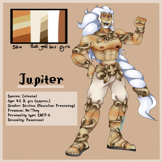
Celestials (PCO) Species sheet!
(This is mostly for my Artfight References, if anyone wants to make an OC with my original species you may! Just credit me pls.)
Celestials, also known as PCB (Personification of a Celestial Body), are living manifestations of Celestial objects ranging from Galaxies, Stars, Planets, in some cases even asteroids, etc. Celestials are all soul-bound to their respective celestial bodies, meaning whatever happens to their counterpart, it affects the Celestial as well, however this is not the case for the other way around. The Celestial itself is immortal, but if they were to be damaged enough, they will only momentarily lose their form and reform in The Kindergarten. The only way to kill a Celestial is to destroy their respective Celestial Body, or wait until they reach the end of their lifespan. The only truly immortal Celestials are Galaxies, which can live forever if not exposed to outside factors such as collision, gamma rays, etc.
Specific details under the cut:
The Kindergarten:
A Celestial is born on a planet known as The Kindergarten as soon as a Celestial Body is formed. The Kindergarten is a large planet located somewhere within Boötes Void and consist of 100% Liquid Starlight, which is what Celestials themselves are made of. Once a celestial body's life officially starts, the planet separates a small portion of Starlight and molds it into a living being. The planet itself is considered alive, or at least sentient. After a Celestial looses their form, their body looses stability, dissolving into liquid and loosing consciousness. They reform back at the kindergarten in a similar process as if they were just born, but keeping all their memories.
The planet itself used to be just an infinite Starlight ocean, but at some point the Celestials decided to build a sort of capitol where Celestials can spend time and connect with others. No other living organism can come to The Kindergarten except when directly brought there by a Celestial.
Another way a Celestial can 'die' is merging, this can happen to any type of Celestial. When two or more celestial bodies collide and merge into one, the Celestials will as well. The resulting Celestial will not have any memories of the previous one, but their personality will be a sort of mix of their previous selves. Not every Celestial sees merging as dying, but some do (Andromeda especially).
Rough appearance of the Liquid Starlight:

Quasarite:
Aside from being bound to their celestial objects, Celestials only have one weakness. Quasarite is a pale purple metal emitting faint purple smoke, it is formed by Quasar activity and is considered one of the rarest materials in the entire universe. It is greatly sought after by both Celestials and living organisms. Physical contact between a Celestial and the material causes an aggressive chemical reaction. A short time exposure causes the skin to bubble and deform and is said to be very painful, but prolonged contact can lead to explosion and the loss of the Celestial's form. If Quasarite gets exposed to liquid Starlight, it gets stained, gaining a very light rainbow-ish tint. Stained Quasarite is way more valuable then the regular variant.
Example of A weapon made of Stained Quasarite: (The SkyPiercer, a scissor blade currently in Andromeda's possession.)

Celestial forms:
The Celestial's body consist of 100% Liquid Starlight, which they can mold and change into any desired shape. They form a translucent glass-like skin that keeps their shape stable after shapeshifting. The appearance of a Celestial depends on multiple factors. Celestials are most known for their adaptability, using their shapeshifting power to mimic the nearest or most interesting looking intelligent organism. Most, if not all, of Celestials make the color of their body the same as the color of the surface of their celestial body. They can change it, but most don't like to look too different than their non living counterpart. Andromeda is kinda an exception. He keeps his colors, but he greatly exaggerates them. The vast majority of Celestials (at least those who have hair) have white hair. The one thing every Celestial have in common appearance wise is having a small replica of their respective celestial object somewhere on their body, the most common place being in place of their head but it varies based on personal preference.
Examples:


Powers:
Many mortal species regard the Celestials as gods or deities, but that is not the case. The only Celestial that can be regarded as a god/deity is The Mother of Everything, the creator of the Celestials. Aside from her, the Celestials regard themselves as just a very advanced species just like any other.
Celestials posses a wide range of powers and abilities, though their power can range based on the overall size or type of their celestial body. Some of the Celestial's powers include:
Shapeshifting
Creation
Clairvoyance
Telepathy
Teleportation
Telekinesis
Force-Field Generation
Healing
Levitation
Material manipulation based on their celestial body type (Ex. planets have earth manipulation, gas giants get air manipulation, etc, etc.)
Another important power they posses is the ability to manipulate the fabric of reality, either by magical manipulation or physically weaving onto it. The Celestials are forbidden by the Mother to do that however and only serves as a last resort when dealing with a powerful force.
The Mother Of Everything:
At the very beginning of this universe, the first Celestial was formed. The Mother of Everything, also known as The Universe, saw herself alone in the world, so it decided to create others like itself to fill the cosmos. She is considered the highest and most powerful of the Celestials, who see her as sort of a mother figure. She is rarely seen anywhere other than where she resides, only leaving due to necessity, a lot of the Celestials go through their whole life without ever seeing her unless they actively seek her out.
It doesn't have a set form, but it has been spotted once or twice in a human-escae form that is comprehendible by mortals:

(Note: I will be updating this anytime I get a new lore idea so this is subjected to change a bit)
#original character#original race#species sheet#original species sheet#original art#digital art#andromeda#artfight#artfight 2025#milky way#jupiter#terra#space#space oc
0 notes
Text
Best Home Tuition Near Me: Discover Excellence with Saraswati Tutorials
Are you searching for the Best Home Tuition Near Me to help your child succeed academically? Whether your goal is to improve grades, prepare for board exams, or build confidence in tough subjects, home tuition offers unmatched benefits—right from the comfort of your home.
And when it comes to trusted, result-oriented private tutoring, Saraswati Tutorials is the name thousands of parents and students rely on for excellence, consistency, and proven results.
Why Home Tuition Near Me is the Smartest Educational Choice
Every child learns differently, and sometimes a school setting isn't enough to address their individual learning needs. That’s why parents are increasingly turning to home tuition near them—because personalized learning leads to better focus, stronger retention, and faster academic growth.
Here’s what makes local home tuition such a powerful learning option:
One-on-one attention from a dedicated tutor
Personalized lesson plans tailored to your child’s pace
Comfort and convenience of learning at home
Improved academic performance in less time
Time-saving—no travel required

Saraswati Tutorials: Best Home Tuition Near You
When you type “Best Home Tuition Near Me” into Google, what you're really looking for is quality, trust, and results. Saraswati Tutorials delivers all three—and more.
Handpicked, Experienced Tutors
Saraswati Tutorials works with qualified, background-verified tutors who specialize in their subjects. From Class 1 to 12 and competitive exams, they provide top-tier coaching in:
Math, Science, English, Social Studies
Physics, Chemistry, Biology
Commerce & Humanities
NEET, JEE, NDA, CUET & more
Local Tutors That Understand Your Board & Curriculum
Whether you're following CBSE, ICSE, or State Board, Saraswati Tutorials assigns tutors who are familiar with your exact syllabus and exam pattern, ensuring maximum impact in minimum time.
Flexible Scheduling & Customized Plans
Morning or evening, weekdays or weekends—get tutoring on your schedule. Choose how many sessions you want per week and adapt it as needed.
Regular Feedback & Academic Monitoring
Saraswati Tutorials goes beyond just teaching—they track progress, conduct monthly evaluations, and offer regular feedback so parents always stay informed.
Subjects & Services Available
ClassSubjectsKey Focus1–5All SubjectsBasic concepts, interactive learning6–8Math, Science, English, SSTStrengthening fundamentals9–10All SubjectsBoard exam preparation, practice tests11–12PCM, PCB, Commerce, ArtsConceptual clarity + Entrance readinessSpecial CoachingJEE, NEET, NDA, CUETCrash courses & mentorship
Available Near You (Pan-Dehradun Coverage)
Saraswati Tutorials provides home tuition near you in every corner of Dehradun:
Rajpur Road
Balliwala
Vasant Vihar
Sahastradhara Road
Jakhan
Dharampur
Premnagar
ISBT and surrounding areas
Wherever you live in Dehradun, Saraswati has a qualified home tutor ready to teach.
Parent & Student Reviews
“We searched for ‘best home tuition near me’ and found Saraswati Tutorials. Within a few weeks, our child’s understanding of Maths improved drastically.” – Mrs. Arora, Sahastradhara
“Our Class 12 tutor was exceptional—punctual, professional, and dedicated. Saraswati is the best tuition service near us.” – Mr. Rawat, Jakhan
How to Get Started
Getting started with the best home tuition near you is simple:
Call or message Saraswati Tutorials
Share your academic needs and subject(s)
Get matched with an experienced local tutor
Start classes at your home within 48 hours
Final Words
Don’t settle for average when the Best Home Tuition Near You is just a call away. With Saraswati Tutorials, you get local, trusted, and experienced educators who bring out the best in your child through personalized attention and proven teaching strategies.
Let Saraswati Tutorials bring top-quality education right to your doorstep. Book your free demo class today!
0 notes
Text
Global Connector Headers Market: Key trends & Forecast to 2032
Global Connector Headers Market size was valued at US$ 2.95 billion in 2024 and is projected to reach US$ 4.87 billion by 2032, at a CAGR of 6.5% during the forecast period 2025-2032
Connector Headers Market Overview
Connector headers are a type of electrical connector commonly used in printed circuit boards (PCBs) for establishing a secure and standardized connection between components. These connectors consist of a row (or multiple rows) of metal pins that are inserted into matching sockets, allowing signals or power to pass between different elements of an electronic system.
Typically mounted directly onto the PCB, connector headers are essential for ensuring efficient signal transmission and providing physical support for detachable connections. They come in various configurations, including single-row and double-row headers, and can be customized for different pin counts, pitches, and orientations (vertical or right-angle).
These connectors are widely used in sectors like automotive, consumer electronics, medical devices, industrial control systems, and more. They are vital in applications that demand compact design, ease of maintenance, and modularity in circuit design.
Their adaptability, low cost, and compatibility with automated assembly processes make connector headers a fundamental component in modern electronics manufacturing.
This report provides a deep insight into the global Connector Headers Market, covering all its essential aspects. This ranges from a macro-overview of the market to micro details of the market size, competitive landscape, development trend, niche market, key market drivers and challenges, SWOT analysis, value chain analysis, etc.
The analysis helps the reader to shape the competition within the industries and strategies for the competitive environment to enhance the potential profit. Furthermore, it provides a simple framework for evaluating and assessing the position of the business organization. The report structure also focuses on the competitive landscape of the Global Connector Headers Market. This report introduces in detail the market share, market performance, product situation, operation situation, etc., of the main players, which helps the readers in the industry to identify the main competitors and deeply understand the competition pattern of the market.
In a word, this report is a must-read for industry players, investors, researchers, consultants, business strategists, and all those who have any kind of stake or are planning to foray into the Connector Headers Market in any manner.
Get Full Report : https://semiconductorinsight.com/report/global-connector-headers-market/
Connector Headers Key Market Trends :
Rising Demand in Automotive Sector: Increasing use of connector headers in electric vehicles and advanced driver-assistance systems (ADAS) is fueling market growth.
Miniaturization of Electronics: The trend toward smaller and more compact consumer electronics is driving demand for miniaturized connector headers.
Growth in Medical Devices: The expanding healthcare industry is adopting connector headers in medical equipment, boosting the market significantly.
Regional Expansion in Asia-Pacific: Asia-Pacific, particularly China and South Korea, is emerging as a major production and consumption hub.
Technological Advancements: Innovations in materials and design, such as high-speed and high-density connectors, are improving product efficiency.
Connector Headers Market Regional Analysis :
North America:Strong demand driven by EVs, 5G infrastructure, and renewable energy, with the U.S. leading the market.
Europe:Growth fueled by automotive electrification, renewable energy, and strong regulatory support, with Germany as a key player.
Asia-Pacific:Dominates the market due to large-scale manufacturing in China and Japan, with growing demand from EVs, 5G, and semiconductors.
South America:Emerging market, driven by renewable energy and EV adoption, with Brazil leading growth.
Middle East & Africa:Gradual growth, mainly due to investments in renewable energy and EV infrastructure, with Saudi Arabia and UAE as key contributors.
Connector Headers Market Segmentation :
The research report includes specific segments by region (country), manufacturers, Type, and Application. Market segmentation creates subsets of a market based on product type, end-user or application, Geographic, and other factors. By understanding the market segments, the decision-maker can leverage this targeting in the product, sales, and marketing strategies. Market segments can power your product development cycles by informing how you create product offerings for different segments.
Market Segmentation (by Application)
Automobile
Medical
Consumer Electronics
Other
Market Segmentation (by Type)
Double Connector Header
Single Connector Header
Key Company
TE Connectivity
Molex
Amphenol-FCI
Samtec
Precidip
Hirose Electric
Harwin
Weidmuller
MPE-GARRY
Panasonic
AVX
3M
Eledis
Elektron Technology
Interplex
Drivers
Increasing Use in Automotive Applications The growing production of electric and hybrid vehicles is driving demand for reliable connector headers, essential for battery management and infotainment systems.
Expanding Consumer Electronics Market The surge in smartphones, laptops, and wearable devices boosts the need for compact and durable connector headers.
Industrial Automation Growth Automation and robotics require efficient connectors for seamless communication between components, enhancing market growth.
Restraints
High Manufacturing Costs The cost of raw materials and complex manufacturing processes may limit market expansion, especially for high-performance connectors.
Supply Chain Disruptions Global supply chain issues, including raw material shortages, can cause delays and increased costs in production.
Stringent Regulatory Standards Compliance with safety and environmental regulations can pose challenges to manufacturers, impacting product development.
Opportunities
Emerging Markets in Asia-Pacific Rapid industrialization and electronics manufacturing in countries like India and China present new growth avenues.
Development of Smart Devices Rising adoption of IoT devices and smart infrastructure increases demand for advanced connector headers.
Sustainable and Eco-friendly Products Growing consumer preference for environmentally friendly components offers opportunities for innovation in biodegradable and recyclable connectors.
Challenges
Intense Competition Among Manufacturers Market fragmentation and aggressive pricing strategies make it challenging to maintain profitability.
Technological Complexity Meeting the evolving technical demands of high-speed data transmission and miniaturization requires continuous R&D investment.
Quality and Reliability Concerns Ensuring long-term durability and performance under harsh conditions remains a challenge for many manufacturers.
Get A Sample Report : https://semiconductorinsight.com/download-sample-report/?product_id=96472
Key Benefits of This Market Research:
Industry drivers, restraints, and opportunities covered in the study
Neutral perspective on the market performance
Recent industry trends and developments
Competitive landscape & strategies of key players
Potential & niche segments and regions exhibiting promising growth covered
Historical, current, and projected market size, in terms of value
In-depth analysis of the Flash Memary Market
Overview of the regional outlook of the Flash Memary Market:
Key Reasons to Buy this Report:
Access to date statistics compiled by our researchers. These provide you with historical and forecast data, which is analyzed to tell you why your market is set to change
This enables you to anticipate market changes to remain ahead of your competitors
You will be able to copy data from the Excel spreadsheet straight into your marketing plans, business presentations, or other strategic documents
The concise analysis, clear graph, and table format will enable you to pinpoint the information you require quickly
Provision of market value (USD Billion) data for each segment and sub-segment
Indicates the region and segment that is expected to witness the fastest growth as well as to dominate the market
Analysis by geography highlighting the consumption of the product/service in the region as well as indicating the factors that are affecting the market within each region
Provides insight into the market through Value Chain
Market dynamics scenario, along with growth opportunities of the market in the years to come
6-month post-sales analyst support
Customization of the Report In case of any queries or customization requirements, please connect with our sales team, who will ensure that your requirements are met.
Related Reports :
Contact us:
0 notes
Text
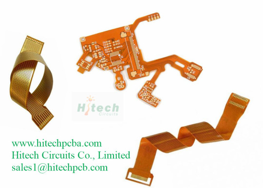
What is Flex PCB?
Flexible printed circuits, also known as flex circuits, are sometimes regarded as a printed circuit board (PCB) that can bend, when in reality there are significant differences between PCB’s and flex circuits when it comes to design, fabrication and functionality. One common mistake that designers make is to design a flexible circuit using the same rules as a PCB. Flex PCB require a unique set-up and have their own set of design rules that the Hitechpcb team has termed “flex-izing” and have worked hard to perfect over the last many years.
Flexible PCB, which also called Flex PCB, Flexible circuit board or flex circuit, it consists of PI base material, adhesive layer, copper layer, coverlay and sometimes with stiffeners. Flexible PCBs are now being used widely to replace traditional FR4 PCB in various different applications due to the benefits from flex PCB specially. Although more expensive than a normal rigid PCB, the right design in the right application could save weight and time in assembly, coupled with the reliability which makes flexible circuit board a worthwhile consideration.
A flexible printed circuit consists of a metallic layer of traces, usually copper, bonded to a dielectric layer, usually polyimide. Thickness of the metal layer can be very thin (<.0001″) to very thick (> .010″) and the dielectric thickness can vary from .0005″ to .010″. Often an adhesive is used to bond the metal to the substrate, but other types of bonding such as vapor deposition can be used to attach the metal.
1 note
·
View note
Text
Exploring the Top Electronic Lab Equipment Suppliers in Indore
Indore, a rapidly growing hub for education, electronics, and industrial innovation, has become home to several advanced technological ventures. Among its rising sectors, electronic lab equipment suppliers in Indore play a pivotal role in equipping educational institutions, R&D centers, and industrial labs with state-of-the-art instruments. Whether you're setting up a new electronics lab or upgrading your testing infrastructure, the city offers a wide range of high-quality equipment suited for various applications.

Why Indore for Electronic Lab Equipment? Indore is recognized for its educational excellence and industrial dynamism. With leading universities, engineering colleges, and a thriving manufacturing base, the demand for lab equipment is constantly on the rise. This has led to a surge in reliable electronic lab equipment suppliers in Indore, offering everything from basic testing tools to advanced embedded systems trainers. Choosing local suppliers ensures better service, faster delivery, and hands-on technical support. Additionally, many suppliers in Indore offer customized training solutions and product demonstrations, making them ideal partners for institutions and companies alike. Types of Products Offered by Electronic Lab Equipment Suppliers in Indore The range of products offered by electronic lab equipment suppliers in Indore is vast and designed to meet the needs of diverse fields. Here’s a breakdown of the major product categories:
Basic Electronics Lab Equipment Power supplies, function generators, and multimeters
Breadboards and prototyping tools
Oscilloscopes and frequency counters
Embedded Systems & Microcontroller Kits Arduino and ARM-based development boards
8051 and PIC microcontroller kits
Training modules for IoT, robotics, and automation
Communication Systems Analog and digital communication trainers
Fiber optic kits
Satellite communication systems
Electrical Engineering Labs Electrical machines, circuit labs, and power electronics kits
Control system simulators
Power system protection and analysis kits
Renewable Energy & Green Tech Solar PV and wind energy trainers
Smart grid simulation units
Energy auditing and monitoring tools
These offerings demonstrate the depth and versatility of electronic lab equipment suppliers in Indore, catering to both conventional and modern curriculum requirements. Key Advantages of Choosing Indore-Based Suppliers Working with electronic lab equipment suppliers in Indore comes with several benefits: Local Support and Service: Having a local presence allows suppliers to offer quick installation, training, and troubleshooting services.
Cost-Effective Solutions: Indore-based vendors often offer highly competitive pricing without compromising on quality.
Customization Capabilities: Suppliers can tailor lab kits based on the institution’s syllabus or industrial training requirements.
Strong After-Sales Support: Dedicated service teams ensure minimal downtime in case of equipment issues.
These factors make the city’s suppliers ideal for long-term academic and industrial partnerships. Applications in Education and Industry The demand for lab equipment from electronic lab equipment suppliers in Indore spans across sectors. Here’s how different industries and institutions benefit: Colleges & Universities: Equip students with hands-on experience in analog, digital, and embedded systems through robust lab setups.
Research Institutions: Perform advanced experimentation and prototyping with precision electronic instruments.
Technical Training Institutes: Offer practical learning environments with real-world tools and scenarios.
Manufacturing Industries: Use high-end lab tools for PCB testing, automation controls, and sensor integration.
Startups & Innovation Labs: Support R&D through rapid prototyping and testing solutions.
The flexibility and reach of Indore’s suppliers make them valuable contributors to academic growth and technological advancement.
Taking these aspects into account ensures that your lab setup is efficient, scalable, and future-ready. Future Trends in Lab Equipment With the rise of Industry 4.0 and smart technologies, electronic lab equipment suppliers in Indore are also evolving. Expect to see integration of: IoT-enabled lab kits
Cloud-based learning platforms
AI-assisted training modules
Virtual simulation labs
These advancements are helping bridge the gap between theoretical knowledge and real-world skills, making technical education more interactive and industry-aligned. Conclusion As education and industry continue to evolve, the need for practical, hands-on learning tools becomes more crucial. Electronic lab equipment suppliers in Indore have stepped up to meet this demand by offering a diverse, high-quality range of lab products tailored for electronics, communication, automation, and renewable energy. By choosing a local supplier in Indore, institutions and businesses gain not only access to top-notch instruments but also technical guidance, training support, and affordable solutions. Whether you're building a new lab or upgrading an existing one, the right supplier in Indore can help you drive innovation, enhance skill development, and stay ahead in today’s competitive landscape.
0 notes
Text
touhou 19 time! this game was literally not even released when i started this, so this is really fresh! this post is probably the closest i will ever be to a real games journalist lol.
nina's thoughts on Touhou 19 - Unfinished Dream of All Living Ghost
the most recent touhou, coming out just a few weeks ago, so this review is hot off the presses! UDoALG (wild abbreviation by the way, this name is so long) is a pretty neat game, being a direct sequel to Wily Beast and Weakest Creature story-wise, and a sequel to Phantasmagoria of Flower View gameplay-wise.
UDoALG is another in the competitive-danmaku type gameplay, similar to PoFV but with a number of evolutions to make the gameplay more balanced and easier to control. i won't go over every little change, since theres quite a lot, but ill point out some interesting changes, mostly in relation to story mode. for starters, Ability Cards are back again from UM, although with a much smaller role. each character has 2 cards themed to them, and whenever you beat an opponent in story mode you're randomly given one of their two cards. the three animal spirits are added, but they work completely differently to WBaWC, now being stronger variants of the generic spirit enemies from PoFV. a change that i think is only in story mode is that a new win condition is added, where if you defeat your opponent's boss summon an amount of times then your opponent loses. this is also pretty much the only wincon in story mode, since the AI has insane dodging skills. i literally only saw them lose a life one (1) time across 19 characters' stories (if you're curious, it was in Chiyari's stage 1).
one really interesting aspect of this game is the storytelling. i usually don't bring up the story in these posts outside of how certain characters relate to it, the story usually is a fairly simple affair that just gives the characters a reason to fight, but UDoALG has a much more complex story, which im kinda mixed on. i'll start with the cool part: the story actually progresses as you play through and unlock various characters in story mode, every set of character unlocks represents a later time period of the story, so you don't get the full story and resolution until you play through it all. this is a super cool idea, and gives good incentive to keep playing different routes and see how it all plays out. its a cool idea that uniquely plays off of the large character roster and unlocking method of these competitive vs games.
unfortunately, in order to make this happen and make every character be relevant, the plot is needlessly convuluted, especially in the first couple campaigns. there are so many factions at play, all with their own motives and double-agents and subterfuge. by the end of the 19 story scenarios you will be absolutely sick of the phrase "this is exactly as i had planned", and yet i still dont fully understand What the "main villain"s plan was. i commend ZUN for trying something new with the narrative, both in doing a direct sequel with most of the same characters as a former game, as well as this way of unfolding the story over time through different character routes, but i can't say it was Good. maybe im just biased since it mostly revolves around the WBaWC cast, and that game already had pretty rough plot and characterization, but i dunno. i will say i liked the story more at the end than i did after doing the first couple routes, but some of that early confusion never really goes away, and characters like Ran and Tsukasa dont really get their stories resolved.
time to talk about the characters! UDoALG is furry city, pretty much every character besides the human incident resolvers is some kind of animal-person, plus a few Onis. for returning characters we have Reimu, Marisa, Sanae, Ran (from PCB), Aunn (HSiFS), Nazrin (UFO), Seiran (LoLK), Rin (SA), Tsukasa (UM), Mamizou (TD), Yachie (WBaWC), Saki (WBaWC), Yuuma (the 3rd Animal Realm leader, coming from a fighting game i think?), and Suika (also a fighting game, and SA). for the new characters, we have 3 new youkai who have each joined one of the animal realm families respectively, plus the 'main villain' Zanmu and her assistant Hisami. since theres only 5 new guys, ill just give them each a quick review.
Son Biten is a monkey youkai, based on Son Wukong, recruited to Yachie's Kiketsu family. she's pretty goofy, and has a really neat musical theme. i dont have much to say about her, besides that she has a cool inspiration, and some of her interactions are pretty funny.
Enoko is a dog-type youkai, loosely based on the idea of Cerberus, who was recruited to Saki's Keiga family. instead of literally having 3 heads, she has bear traps on her wrists that act as analogues to the jaws of two additional heads, which is a really neat interpretation of a cerberus concept, as well as having tons of comedic potential. i love all the jokes people make about her offering up a Totally Normal Handshake, dont worry about it. she apparently lived in the Forest of Magic as a dog before awakening as a youkai, so she joins the crew of Marisa's funny forest friends.
the third new Youkai is Chiyari, who is NOT a chupacabra, despite what everyone says. she's based on a Tenkajin, which is apparently an obscure youkai that sucks blood, obscure enough that i could only find a single source for it online, being a Japanese blog post written by who i assume is a youkai enthusiast. Anyways, nobody in Gensokyo knows what a tenkajin is either, so everyone calls her a chupacabra instead since its another bloodsucking creature who is 'pretty popular right now'. most of her interactions are her being annoyed by being called a chupacabra, and eventually coming to terms with it. poor tenkajin gets no respect. shes very funny, and also apparently completely broken in pvp. great character.
Hisami is a 'guide of Hell', who is also inexplicably based on grapes for some reason (or eggplants, depending on who you ask, but im in grapes camp.) she pretty much just finds people in hell and helps them find their destination, although 'their destination' is up to Hisami's interpretation, and multiple times in the story she leads characters somewhere else. apparently she does her job wrong because she wants Zanmu to notice her, and it doesn't work cause apparently that was part of Zanmu's plan all along, so she doesn't care. Zanmu is too busy playing 4d chess to give her suboordinate some attention, so sad.
speaking of, Zanmu is an Oni, and the 'main villain' of the game. i say that with quotes because, despite being the final boss in most routes, and being the chessmaster supposedly laying out the big plans and manipulating everyone, she also is simultaneously resolving the incident, kinda?? its a bit hard to understand her motivations. well i guess her motivations make sense, but its hard to understand how exactly she plans to get what she wants from this plan. like her plan involves getting beat up by Reimu multiple times? hello?? not a fan, and she doesn't even have a cool design inspiration to make up for it, shes just another oni.
alright, lets wrap this one up. i was surprised to see another VS type game come out, and it seems to deliver a lot more balanced and interesting combat than the first one (granted, story mode plays pretty differently from what i can tell). the story is weird though, and the roster doesn't really have many characters i'm excited to play as compared to PoFV, and the characters i do like are pretty bad. (Sanae in particular is really weak in this format, her homing snakes are a huge disadvantage against bosses since they turn as soon as they see an enemy, meaning they wont hit the boss unless every random spirit or fairy is dead first). complaints aside though, at the base level its still pretty fun, and im glad that this type of gameplay is being given another chance.
i said it in my PoFV review, and ill say it again here: if any of you reading this have UDoALG, and are interested in playing the PvP with me, hit me up! itd be fun to try playing this with another person (although i heard the online is rough so i dunno…)
thank you so much for reading, especially those of you that have stuck with me through each post! this is the end of the mainline series, but there's still a lot out there i havent done. im not sure where this will go from here, especially since my college semester just started so i'll have a lot less free time, but ive had a lot of fun working on this project, and i hope that youve had fun reading it! if i do keep going, i might do the PC-98 quintilogy next, or maybe talk about cool fangames like Luna Nights or Mystia's Izakaya, i dunno. whatever comes next though, i hope to see you again! consider this the end of 'volume 1' of my grimoire. farewell!
#grimoire of nina#touhou#touhou 19#touhou UDoALG#unfinished dream of all living ghost#touhou project#touhou 19 spoilers
6 notes
·
View notes
Text
Radiology Courses in Nashik: Complete Guide

🔍 What is Radiology?
Radiology is the science of using medical imaging to diagnose and sometimes treat diseases. From X-rays to MRIs and CT scans, radiologists are the detectives of the medical world — they see what others can’t. They interpret images that help doctors make crucial decisions. Check out different radiology courses in Nashik below for a better and bright future.
🎯 Why Choose Radiology?
Radiology is a fast-growing field with ever-advancing technology. If you love medicine and technology and want a role that’s both analytical and clinical, radiology might just be your calling.
📚 Overview of Radiology Education in India
✅ Eligibility Criteria
To pursue a radiology course:
For Diploma: 10+2 with Science (PCB)
For UG: 10+2 with minimum 50% marks in PCB
For PG: MBBS or equivalent degree
🎓 Types of Radiology Courses
Radiology courses come in different formats:
Certificate Courses (6 months - 1 year)
Diploma Courses (1-2 years)
Undergraduate Courses like B.Sc. in Radiology (3 years)
Postgraduate Courses like MD in Radiology or PG Diploma (2-3 years)
📍 Radiology Courses in Nashik
📄 Certificate Courses
Short-term, focused training courses ideal for technicians and support staff.
📄 Diploma Courses
Examples:
Diploma in Radiological Techniques
Diploma in Medical Imaging Technology
📄 Undergraduate Courses
B.Sc. in Radiology & Imaging Technology
Duration: 3 years
Includes theory and practicals
📄 Postgraduate Courses
MD in Radiology
PG Diploma in Radiodiagnosis
🏥 Top Colleges Offering Radiology Courses in Nashik
🏫 MVP Samaj's Dr. Vasantrao Pawar Medical College
One of the most reputed medical colleges in Nashik offering diploma and MD programs in Radiology.
🏫 SMBT Institute of Medical Sciences
Known for its high-end diagnostic labs and practical-oriented teaching.
🏫 Ashoka Institute of Medical Sciences
Emerging institute with modern radiology equipment and B.Sc. programs.
📘 Course Curriculum and Subjects
📗 Key Topics Covered
Human Anatomy & Physiology
Radiographic Physics
Imaging Techniques (X-ray, MRI, CT)
Patient Care & Ethics
📘 Practical Training
Hands-on experience is crucial. Students work with imaging machines and learn to interpret results under expert supervision.
📝 Admission Process
📋 Entrance Exams
NEET-UG for MBBS-based courses
CET for some diploma/UG courses
📋 Direct Admission Options
Many private institutes in Nashik offer direct admissions based on merit or management quota.
💼 Career Opportunities After Radiology Courses
🏥 Jobs in Hospitals and Diagnostic Centers
You can work as:
Radiologist
Radiologic Technologist
MRI/CT Technician
Diagnostic Medical Sonographer
🎓 Scope in Research and Academia
Colleges, research labs, and public health initiatives need radiology professionals for academic and investigative work.
💰 Salary Expectations
💸 Entry-Level Salary
A fresh radiographer can expect ₹2.5 to ₹4 LPA. Those with an MD in Radiology may start at ₹8-12 LPA.
📈 Growth with Experience
With experience and specialization, the salary can go up to ₹25 LPA or more, especially in corporate hospitals and private diagnostics.
🧠 Skills Required to Succeed in Radiology
🛠️ Technical Skills
Operating complex imaging machines
Image interpretation
Radiographic positioning
🗣️ Soft Skills
Attention to detail
Communication
Patience and empathy with patients
🎓 Internship and Hands-On Experience
Most courses require 6 months to 1 year of internship. This real-world experience is vital for skill-building and confidence.
🏛️ Government vs. Private Colleges – What’s Better?
Govt Colleges: Affordable, strict merit-based admissions, limited seats.
Private Colleges: Modern infrastructure, easier admission, higher fees.
🌐 Online Radiology Courses – Are They Worth It?
While practical skills are best learned in person, online courses are great for theory, updates on recent advancements, and certifications.
🔮 Future of Radiology in India
AI and advanced imaging technologies are transforming the landscape. The demand for radiology experts is rising in both urban and rural areas.
💡 Tips for Aspiring Radiologists
Stay updated with the latest imaging technologies.
Practice image interpretation regularly.
Choose a course with good clinical exposure.
Build a strong network with medical professionals.
✅ Conclusion
Radiology is a dynamic and vital part of the healthcare system. If you’re looking to enter a field that combines technology, patient care, and scientific reasoning — radiology is worth exploring. Nashik offers a good mix of colleges and training facilities for aspiring radiologists. Whether you’re just starting or looking to specialize, the path is full of exciting possibilities.
❓ FAQs
Q1. What is the best radiology course in Nashik? The MD in Radiology from Dr. Vasantrao Pawar Medical College is highly reputed.
Q2. Can I pursue radiology after 12th Science? Yes, you can apply for diploma or B.Sc. radiology courses after 12th with PCB.
Q3. Is NEET required for radiology courses? Only for MBBS-based or postgraduate medical programs. Not required for B.Sc. or diploma.
Q4. Are there good job opportunities in Nashik after a radiology course? Yes, many private hospitals and diagnostics centers offer placements in and around Nashik.
Q5. What is the fee range for radiology courses in Nashik? It varies — ₹50,000 to ₹2,50,000 annually depending on the course and institution.
0 notes
Text
Hitech express prototype PCB assembly manufacturing is a specialized service that enables us to take complicated PCB fabrication, components souring and prepare them for assembly and testing. As the top PCB manufacturer in the China, Hitech Group can fulfill your prototype and production needs. We understand that bringing a product to market in a timely and cost effective manner can mean everything in business. Our quality, experience, service and pricing combine to become your efficient and reliable electronic supplier.
We use the latest equipment to assembly complex PCBs as promptly as possible – often with 24 hours. We are setup specifically for deal with fast turn electronics assembly and all the issues that go hand in hand with the process, giving us an upper hand over most manufacturers, our team is capable of manufacturing prototype printed wiring board assembly volumes of 1-50 pieces.
Our knowledgeable and experienced staff have the know-how and equipment to be able to deal with any project you care to send our way – no job is too demanding. We can guarantee we will deliver exactly what you need with both speed and quality, so you can rest easy knowing you’re in good hands.
The benefits of PCB prototype assembly The reason for ordering a PCB prototype is that you want to quickly assess how your PCB design will work. This cannot be achieved without going through the board assembly process. Fortunately, HitechPCB can complete the assembly of PCB prototypes internally, so you can quickly understand the working condition of the assembled PCB prototypes.
There is no need to manufacture it here and then look for a prototype PCB assembly expert. This will take too long and go against the purpose of making a PCB prototype from the very beginning. Work with HitechPCB and let us get all of this done for you quickly.
PCB prototype assembly with the same high-quality standards Although prototype assembly is usually composed of limited production runs, we bring the same high quality and care to the entire process of our production assembly projects. We utilize the same resources and personnel to ensure the best outcome. Our capable team is fully qualified to handle all aspects of the process, including the procurement of PCB parts and electronic components, circuit board manufacturing, PCB assembly manufacturing and quality control. We will also design according to your original PCB prototype. We won't make any modifications without your consent. Our services include Design for Manufacturers (DFM) capabilities and Design for Testing (DFT) to ensure that your PCBA prototype complies with your exact design specifications. We can even assemble prototypes of high-density FR-4 circuit boards.
The prototype PCB assembly has a competitive price HitechPCB offers many methods to minimize the assembly cost of your PCB prototype. When it comes to all your PCB solutions, we are the best choice, including printed circuit board manufacturing, PCB component procurement and prototype circuit board assembly requirements. Because all of our work is done internally by our well-trained team of engineers and design experts, you know you will get a smooth and effective communication process, which will lead you to the prototype you want. You or your management team will not be bound by logistics and try to have the design company communicate with the manufacturer. To obtain the PCB prototype assembly quotation for your custom PCB project, please send us the relevant circuit specifications and BOM files. We will provide the PCB assembly price within 24 hours.
Quotation for PCB assembly within 12 holes for urgent projects A PCB assembly is a circuit board that contains all the necessary components. Various factors, such as the quantity of different parts, the type of PCB components and services, determine how you obtain quotations for PCB components. Under normal circumstances, many suppliers' PCBA quotations take more than five days. However, we have many experienced staff members who can send you PCB assembly quotations within 12 holes and urgent project quotations.
Hitech PCB provides SMT assembly services for our printed circuit board customers. We will provide you with a quotation in a very short time and purchase components according to your BOM list. We offer competitive prices for PCBA services, such as our PCBS. All your projects can be completed under one roof: PCB manufacturing, assembly, PCBA testing!
To obtain a quick turnover PCB component quotation, you need to provide these data. Gerber files, BOM lists, Q 'ty, test programs, required delivery dates, delivery addresses, etc.
Welcome to choose Hitech Group as your PCB, electronic assembler and PCB assembly manufacturer. For bare PCBS with fast turnaround
0 notes