#What is a Schottky diode
Text
What is a Schottky Diode, Schottky barrier diodes, Schottky diode
ZHCS1000 Series 1000 mA 40 V 100 uA High Current Schottky Barrier Diode - SOT-23
#Diodes#Schottky Diodes#ZHCS1000TA#Diodes Incorporated#What is a Schottky Diode#Schottky barrier diodesTypes of RF Diodes#hot carrier diode#semiconductor diode#diode manufacturers#diode chip#higher switching speed#voltage drop
1 note
·
View note
Text
Junction diode, RF Diodes, what is a Schottky Diode, hot carrier diode
BAT54W Series 30 V 600 mA Surface Mount Schottky Barrier Diode - SOT-323
#Diodes Incorporated | BAT54CW-7-F#Diodes#Schottky Diodes#Junction diode#RF Diodes#what is a Schottky Diode#hot carrier diode#Schottky diode chip#higher switching speed#Semiconductor diode#low voltage diode#Schottky diode voltage drop
1 note
·
View note
Text
B290 series 90 V 2 A High Voltage Schottky Barrier Rectifier - DO-214AA, SMB
#Diodes#Schottky Rectifiers#B290-13-F#Diodes Incorporated#High speed switching#Schottky barrier diode#Power supplies#hot-carrier diode#What is a Schottky diode#Schottky diode rectifier#schottky barrier rectifiers#power schottky rectifier#High Voltage Schottky Barrier Rectifier
1 note
·
View note
Text
https://www.futureelectronics.com/c/semiconductors/discretes--diodes--scottky-rectifiers/products
Rectifiers have many uses and are often found serving as components of high-voltage direct current power transmission systems and DC power supplies. Fast rectifier diodes feature very low reverse recovery time, very low switching losses and low noise turn-off switching.
#Nexperia#PMEG6010EP#115#Diodes#Schottky Rectifier#B340B-13-F#Diodes Incorporated#Schottky diode voltage drop#schottky diodes#Semiconductor diode#what is a Schottky Diode#Schottky barrier diodes#Schottky diode manufacturers
1 note
·
View note
Text
RF Diodes, Surface Mount Schottky Power Rectifier, high frequency,
PDS5100 Series 100 V 5 A High Voltage Schottky Barrier Rectifier - PowerDI-5
#Diodes#Schottky Rectifiers#PDS5100-13#Diodes Incorporated#schottky bridge rectifier#MEGA Schottky Barrier Rectifier#what is a Schottky#power circuits#Power management circuits#RF Diodes#Surface Mount Schottky Power Rectifier#high frequency
1 note
·
View note
Text
Schottky barrier rectifiers, High Voltage Schottky Barrier Rectifier, Switching Diodes
PDS5100 Series 100 V 5 A High Voltage Schottky Barrier Rectifier - PowerDI-5
#Diodes Incorporated#PDS5100-13#Diodes#Schottky Rectifiers#power management circuits#Recovery diode#High Voltage Schottky Barrier Rectifier#Switching Diodes#What is a Schottky rectifier#power supplies#TV tuners#high frequency
1 note
·
View note
Text
What is the Schottky diode, semiconductor junction diode, ow voltage-drop
BAT54W Series 30 V 600 mA Surface Mount Schottky Barrier Diode - SOT-323
#Diodes#Schottky Diodes#BAT54CW-7-F#Diodes Incorporated#what is the Schottky diode#semiconductor junction diode#hot-carrier diode#low voltage diode#fast switching action#voltage drop#Schottky barrier diodes#power Schottky diodes
1 note
·
View note
Link
0 notes
Text
https://www.futureelectronics.com/c/semiconductors/discretes--diodes
A diode is an electronic component with asymmetric transfer characteristic, with low resistance to current flow in one direction, semiconductor diode is a crystalline piece of semiconductor material.
#What is a Diode#RF Diodes#hot carrier diode#switching diode#Bridge Rectifiers#Schottky Diodes#Switching Diodes#Current Limiting Diodes#Schottky Rectifiers#Tuning/Varactor Diodes#Fast Rectifiers#Zener Diodes#Small Signal Diodes#Ultrafast Rectifiers#PIN Diodes#Standard Rectifiers
1 note
·
View note
Text
I'm this close to giving up. I have this electronic circuit that I'm building, and I have an example for it. The example works, I've built a copy on a breadboard. The only question I have is: Why? Why does it work?
I am specifically talking about this:

This is from RCN-217, a model railroad standard, and it's not the full schematic, just the part that vexes me; specifically D2 and D3, R1 and R2, and C4.
For context, in this model railroad standard, X2-1 and X2-2 receive a square AC-like waveform, 15 Volts give or take, with plus and minus changing between X2-1 and X2-2 at a rate of around 8kHz (the specific frequency is variable, that's how information is encoded here).
D1, C1-C3 and IC3 just generate +5V DC, using half-wave rectification. Thanks to D1, C1 only gets charged when X2-1 is high and X2-2 is low. That's fairly simple. I had to use a Schottky diode (1N5819) for D1 on my breadboard because I was getting overcurrent faults from my model railroad control system otherwise, but that's about it.
Then there's the part below the X2-2 line (which has been declared ground for this circuit). It generates a small negative voltage (relative to GND). On the right-hand side of the circuit, this is used for an Op-Amp in a fairly straightforward way. The voltage it generates is equal to -Uf of D2 (and D3), about -0.7 Volts, and there's a voltage divider in the rest of the schematic that generates -18 mV (according to labels) from this, which fits exactly.
I have found another similar design for the same purpose which uses (double) Schottky diodes for the equivalent of D2 and D3, and a few different values for capacitors. Its voltage divider assumes that the resulting voltage is about -0.5 volts, so again, that seems like it's Uf of the diodes… but that's just my guess.
So where does this voltage come from?
As far as I can tell so far:
Assume X2-1 is high, X2-2 is low. Then thanks to D3 and D2, nothing of interest happens.
Now X2-1 is low and X2-2 is high. D3 and D2 are open, and the voltage at the negative pin of C4 should be half the voltage between the different rails (so about -7.5V relative to GND), which charges it up.
Then D2 and D3 close again, so at the end of R2 we get around -7.5 V (actually I'm probably wrong about that, shouldn't D2 still be open and discharge C4 via R2?)
Except we don't, because I'm making either a tiny or a fundamental mistake here.
What I actually get at the negative side of C4 is about -4.2 V, and that's fairly constant according to my oscilloscope.
I know this is some kind of charge pump, but this doesn't really match anything I know about charge pumps (which isn't a lot anyway)
I could just copy the design and just assume everything works out, but I actually really would like to know what's happening there, mostly so I know the voltages for the voltage dividers are correct.
2 notes
·
View notes
Text
Occasionally in all my work towards building my Eurorack system into what could really termed a modular synthesizer, I forget that I do, in fact, already own a modular synthesizer.

This is the nucleus of that system: The Korg/Little Bits Synth Kit.
Little Bits, if you're unfamiliar, is a series of educational electronics kits, aimed at children. It works by stringing modules together — they snap together using magnets — and passing a signal down the road of Bits. In a simple electronics context, you'd have your power supply — the blue-edged module on the upper left — followed by a sensor, like a light sensor or a noise sensor; you'd then connect things to act on the signal created by that sensor. You might scale it by putting it through a slider, and then send it into a Bit that lights up, or turns a servo motor.
The synthesizer takes this model and applies it as a volt-per-octave voltage controlled synthesizer. You can use the piano keyboard Bit to push the keys of a tune directly, or the sequencer Bit to program in a little loop; pass that to an oscillator Bit, and it's playing notes. There's a filter Bit, based on the MS-20, and a envelope Bit (really a VCA with a built-in attack-release envelope generator), and even a delay to add reverb or echoes. You pop the speaker onto the end and play things out loud or through the headphone jack.

I've accumulated quite a few Bits; this selection is most of my musical ones. The original set I got at a heavy discount when Radio Shack closed its stores, and I got a second set of many of the synth modules in a set that wound up at a local outlet store's toy aisle, while others came from thrifting. I paid full price for the Arduino Bit — a complete Arduino Leonardo compressed into a tiny module with magnet connectors — but I'm pretty sure everything else was pretty inexpensive.
But I saw the other day that the manufacturer sells a CV Bit — a Bit with a pair of 3.5mm jacks, that let you plug your Bits into a Eurorack signal chain. And I might still get that, as it'd be very useful to use with chains of Bits. But what about just using one Bit at a time? Like, dropping the Filter Bit in, and having jacks for both the inputs and the output?

Here's the test panel. I have a couple of what are called Wire Bits — just the magnet connectors and the power, ground, and signal on a set of wires between them. The idea is to wire them up so the module provides 5v power and grounding, and connects the signals to jacks — in 1 for the top, in 2 for the side (used for control or gate signals), and out for the bottom. I have it here hooked to a Filter Bit. It's unwieldy at 8HP — the Bit kinda dangles out there — but it'll work okay.
The only reason it's still a mockup is my concern about passing the Bits more voltage than they can handle, or different voltage than they can handle. The signal is supposed to fluctuate between 0v and +5v, but Eurorack signals can, depending on the module, cover a wider range than that; -5v to +5v is common, and up to ±10v or even ±12v isn't impossible. So modules have to consider protecting their inputs, and I don't know what protection Little Bits have already. I probably should just put in some sort of diode clamp on the input jacks — I'm told that Schottky diodes to both +V and ground, plus a small series resistor, should do the trick.
4 notes
·
View notes
Text
What is a FRAM
My study is to know more about Diodes Incorporated, B290-13-F, Diodes, Schottky Rectifiers, Power thyristor and What is a FRAM
0 notes
Text
What makes Onsemi diodes stand out from other brands?
Exceptional Quality and Reliability One of the standout features of ON Semiconductor diodes is their exceptional quality and reliability. ON Semiconductor is renowned for its stringent quality control measures and robust manufacturing processes, ensuring that each diode meets the highest standards of performance and durability. This commitment to quality has earned ON Semiconductor a reputation for reliability, making their diodes the preferred choice for critical applications where performance is paramount.
Wide Range of Diode Types and Packages ON Semiconductor offers a comprehensive range of diodes to suit various applications, including rectifiers, Schottky diodes, Zener diodes, TVS diodes, and more. Whether you need a diode for power supply rectification, voltage regulation, or transient voltage suppression, ON Semiconductor has you covered. Additionally, ON Semiconductor diodes are available in a variety of packages, including surface-mount and through-hole options, making them suitable for a wide range of design requirements.
Cutting-Edge Technology and Innovation ON Semiconductor is at the forefront of semiconductor technology, constantly innovating to meet the evolving needs of the electronics industry. Their diodes incorporate the latest advancements in semiconductor technology, ensuring optimal performance, efficiency, and reliability. Whether it's reducing leakage currents, improving switching speeds, or enhancing thermal performance, ON Semiconductor diodes are designed to deliver superior performance in the most demanding applications.
Environmentally Friendly Solutions In addition to their performance and reliability, ON Semiconductor diodes are also environmentally friendly. ON Semiconductor is committed to sustainability and environmental responsibility, and their diodes are designed with these principles in mind. ON Semiconductor diodes are lead-free and comply with RoHS regulations, making them a greener choice for environmentally conscious designers and manufacturers.
Global Presence and Support ON Semiconductor has a global presence, with manufacturing facilities, sales offices, and distribution centers around the world. This global reach ensures that ON Semiconductor diodes are readily available wherever you are, and their extensive network of sales and support professionals is always on hand to provide assistance and technical expertise. Whether you need help selecting the right diode for your application or troubleshooting an issue, ON Semiconductor's global support network has you covered.
0 notes
Text
https://www.futureelectronics.com/p/semiconductors--discretes--diodes--scottky-rectifiers/pds5100-13-diodes-incorporated-6129425
What is Diode, high frequency, high Voltage Schottky Barrier Rectifier
PDS5100H Series 100 V 5 A High Voltage Schottky Barrier Rectifier - PowerDI-5
#Diodes Incorporated#PDS5100-13#Diodes#Schottky Rectifiers#High speed rectifier diodes#Microwave diode#RF Diode#high frequency#high Voltage Schottky Barrier Rectifier#circuit#Recovery diode#Schottky bridge rectifier#rectifier chip
1 note
·
View note
Text
Review, teardown, and testing of LRS-150-24 Mean Well power supply
The LRS-150-24 power supply can operate from a 100–120 volt or 200–240 volt AC network. The manufacturer states it provides an output current of up to 6.5 amperes at 24 volts. The supply measures 5¾ × 3¾ × 1¼ inches (145 × 95 × 30 millimeters), made on a fiberglass printed circuit board fixed to the base's case. The top cover is perforated in a honeycomb pattern. The case and cover are both made of aluminum.
The board is put together neatly, with no visible defects. The components are arranged evenly, and soldering was done with a no-clean flux. Absolutely nothing dangles or rattles in the assembly.
No noises of any sort were noticed during the operation of the power supply.
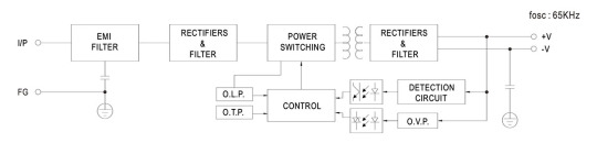
The power supply uses a flyback circuit without PFC.
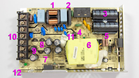
The input voltage is supplied to the input node: RF interference filter (1), a pulse surge limiter (varistor), then the voltage goes to the diode bridge (2) and two input electrolytic capacitors (3). The input voltage selector is also located here. Flyback, built on a MW03A controller (4, installed on the back side of the board) and a power switch (5) on a N-channel MOSFET transistor MMF60R290P. Unfortunately, there is no information about the controller on the Internet. The transistor has a channel resistance of 0.29 ohms at 650 volts and 13 amps. The transformer (6) is entirely covered by the casing, so it is unclear what core material is used. The output rectifier (7) is built using a Schottky diode HBR20150 in a TO-220F package screwed to the side wall and covered with casing. It is basically dual 150V 10A diodes connected in parallel. After the diode there are four output electrolytic capacitors (8) and an additional LC filter. Here (12), there is a small output voltage indicator (green LED) and a regulator (tuning resistor) for adjusting the output voltage. Input and output circuits are connected through a shared screw 7-terminal block (10). 3 terminals for the input line, neutral, and ground wires, and 2 in parallel for common and +24V output.
The main electrolytic capacitors are designed for operating temperatures up to 220°F (105°C), Rubycon. Two optocouplers (11) are installed in the feedback circuit, most likely with phototransistors transmitting control signals from the low-voltage output to the high-voltage input side.
The board has a few cutouts to increase the dielectric strength between the high-voltage and low-voltage sides of the circuit.
The picture shows that the board has three unused spots for storage output capacitors (8), most likely used in the other power supplies of the same series but with different output voltages.
Test conditions
Most tests use metering circuit #1 (see appendices) at 80°F (27°C), 70% relative humidity, and 29.8 inHg pressure.
The measurements were performed without preheating the power supply with a short-term load unless mentioned otherwise.
The following values were used to determine the load level:

Output voltage under a constant load

The high stability of the output voltage should be noted.
Power-on parameters
Powering on at 100% load
The power supply is turned off at least 5 minutes before the test, with a 100% load connected.
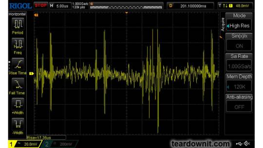
The oscillogram of switching to a 100% load is shown below (channel 1 is the output voltage, and channel 2 is the current consumption from the grid):
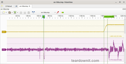
The picture shows three distinguishable phases of the power-on process:
The pulse of the input current charging the input capacitors when connected to the grid has an amplitude of about 7.5 A and a duration of 2 ms.
Waiting for the power supply control circuit to start for about 100 ms.
(Output Voltage Rise Time) Starting the converter, increasing the output voltage, and entering the operating mode) is 8 ms.
(Turn On Delay Time) The entire process of entering the operating mode from the moment of powering on) is 119 ms.
(Output Voltage Overshoot) Output voltage overshoot is absent; the switching process is aperiodic.
Powering on at 0% load
The power supply is turned off at least 5 minutes before the test, with a 100% load connected. Then, the load is disconnected, and the power supply is switched on.
The oscillogram of switching to a 0% load is shown below:
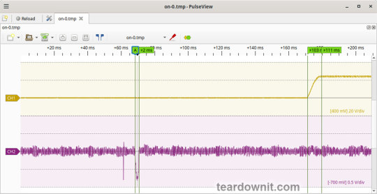
The picture shows three distinguishable phases of the power-on process:
The pulse of the input current charging the input capacitors when connected to the grid has an amplitude of about 7 A and a duration of 2 ms.
Waiting for the power supply control circuit to start for about 103 ms.
(Output Voltage Rise Time) Starting the converter, increasing the output voltage, and entering the operating mode) is 8 ms.
(Turn On Delay Time) The entire process of entering the operating mode from the moment of powering on) is 111 ms.
(Output Voltage Overshoot) Output voltage overshoot is absent; the switching process is aperiodic.
Power-off parameters
The power supply was turned off at 100% load, and the input voltage was nominal at the moment of powering off. The oscillogram of the shutdown process is shown below:

The picture shows two phases of the shutdown process:
(Shut Down Hold Up Time) The supply continues to operate due to the input capacitors holding charge until the voltage across them drops to a certain critical level at which maintaining the output voltage at the nominal level becomes impossible is 31 ms.
(Output Voltage Fall Time) Reduction of the output voltage, stopping voltage conversion, and accelerating the voltage drop is 21 ms.
(Output Voltage Undershoot) Output voltage undershoot is absent, and the shutdown process is aperiodic.
Ripple voltage and current
100% load
The diagram of the current draw from the grid at 100% load is shown in the oscillogram below. The amplitude of the current is about 7.5 A:
Low-frequency output voltage ripple is under 30 mV (see the oscillogram below):

Output voltage ripple at the converter frequency is under 30 mV (see the oscillogram below):

75% load
Output voltage ripple at the converter frequency is under 30 mV (see the oscillogram below):
Low-frequency output voltage ripple is under 30 mV (see the oscillogram below):

50% load
Output voltage ripple at the converter frequency stays below 10 mV; see the oscillogram (11):
10% load

0% load
No-load current consumption was measured with a multimeter, which is 60 mA RMS.
(Power Consumption) The first assumption of excessive standby power draw of more than 7 W is wrong since the current in this mode is predominantly reactive. Indeed, the input filter in the circuit contains two capacitors with a capacitance of 0.68 μF each; these low-frequency capacitors are connected in parallel, i.e., an equivalent capacitance of 1.36 μF is connected to the input terminals. A simple calculation shows that the current through these capacitors should be equal to Ic=120×2×pi×60×1.36e-6=61.5 mA. A slight difference from the measured value can be explained by the deviation of the actual parameters from their nominal values and measurement error.
Measuring the exact active power consumption at a 0% load with a basic set of instruments (oscilloscope, multimeter, etc.) is impossible.
Output voltage ripple at the converter frequency is under 20 mV (see the oscillogram below):

The amplitude of low-frequency output voltage ripples is about 25 mV (see the oscillogram below):

Dynamic characteristics
A mode with periodic switching between 50% and 100% load was used to evaluate the dynamic characteristics. The process oscillogram is shown below (17):

It is evident that the supply’s response to loading changes is close to aperiodic, and there is no overshoot, which indicates a good stability margin. The magnitude of the response to load changes is within 200 mV.
Overload protection
The claimed protection type is "hiccup mode, recovers automatically after fault condition is removed". This was confirmed during testing. When a short circuit occurs, the power supply periodically tries to turn back on and, if the overload is still present, turns off again until the next attempt. This operating mode reduces energy losses and heating during overload. Still, it does not allow the parallel connection of multiple power supplies with a common output.
The output current for the overload protection to kick in is 8.5 A.
Input circuit safety assessment
(Input discharge) Safety assessment is based on the discharge time constant of the input circuits when disconnected from the grid; the value is 0.384 s. This means that when operating on a 120 V input voltage, the time required to discharge the input circuits to safe values (<42 V) will be 0.61 s:

Important: The result is valid for this particular power supply unit; it was obtained for testing purposes and should not be taken as a safety guarantee.
Thermal modes
When operating with no load connected, no component overheating had been noticed.
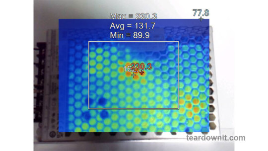
When operating under load, the input diode bridge heats up most noticeably.
With a load of 90% and the top cover closed, the case heats up to approximately 200°F; the hottest spot is located in the area of the diode bridge rectifier.
With a load of 95% and the lid closed, the case temperature reaches 230°F:
The temperature of the bridge rectifier itself is a dangerous 250°F:
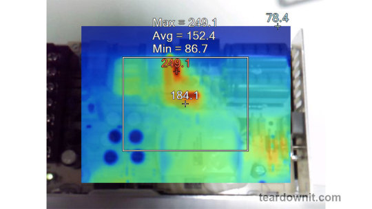
Somewhere around these load values, the power supply goes into a pulse-power-limiting mode and remains in this state either until the load drops or until it cools down. Then this 'heat up', 'limit power', 'cool down', and 'turn back on' cycle repeats.
Other things to consider:
Hot summer weather will decrease the maximum sustainable power output this supply can provide even more.
The tests were conducted with unobstructed air access to the housing for cooling; any changes may increase the heating.
This means that the power supply cannot handle its rated load for a prolonged period with no forced ventilation, and the load should be limited to 5.5 or even 5.0 A.
Conclusions
The reviewed power supply unit has characteristics generally consistent with those declared by the manufacturer, except for the long-term output power, which should be around 120 W.
The build quality is decent; no components clearly unsuitable for the general application, power draw, current, voltage, or temperature were found in the circuit.
The stability of the output voltage should be especially noted.
0 notes
Text
What is a Schottky Diode, Types of RF Diodes, hot carrier diode, diode
BAT54SW Series 30 V 600 mA Surface Mount Schottky Barrier Diode - SOT-323
#Diodes Incorporated#BAT54SWQ-7-F#Diodes#Schottky Diodes#Fast switching#manufacturers#RF diode#Schottky barrier diodes#Types of RF Diodes#hot carrier diode#Schottky diode chip#higher switching speed#Schottky diode voltage drop
1 note
·
View note
Last Seen Blogs

ecosmiing
ECOS - Crypto investment platform

lufesabika
Untitled


feebleistik
Lae’zel Apologist And Supporter

survivorsuriname
Tumblr Survivor Suriname