#led epi wafer
Text

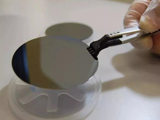
Silicon EPI wafer is an exotic semiconducting material. It is combined with epitaxial growth that is a deposition of a crystalline layer over a crystalline-based semiconductor substrate, called silicon EPI wafer. These wafers are used as a high purity layer and for the formation of thick dopes. An epitaxial wafer is used for photonics, microelectronics, spintronics, or photovoltaics in various application such as smart phones, LED, gyroscope, laptops, tablets, gaming consoles, and others.
0 notes
Text
Overview on Epitaxy and its Applications
Epitaxy
Derived from the Greek word epi, which means above, and taxis which indicates an ordered manner. The LED Epi wafer is very reliable. This process forms one or several crystalline thin films that can be of the same or different chemical compositions and it has the structure as the substrate. In the technique of crystallography where natural or artificial crystals are grown on a crystalline substrate, Epitaxy is an important technique that is used.
In nanotechnology and semiconductor fabrication the process is used where it is of commercial importance. Epitaxy is the only affordable method for many semiconductor materials where high-quality crystals are growing. It marks little importance for most thin-film applications, for example, hard or soft coatings, or optical coatings whereas in semiconductor thin-film technology it is critical. In this in electronic and photonic devices such as computer video displays and telecommunication applications, the growth of semiconductor materials forms layers and quantum wells. For maximum technological applications, the desire is for the deposited material to form a crystalline film that concerning the substrate crystal structure has one well-defined orientation. You can purchase wafers from LED Epi wafer supplier.
Applications and Epitaxial Growth of Thin Film Materials
In electronics, optoelectronic and magneto-optics epitaxial growth of thin-film materials has numerous applications. In several ways, growth can occur where the most common is the vapor phase epitaxy (a modification of chemical vapor deposition), where from vapor the atoms for deposition on the substrate are taken and growth occurs at the gaseous/solid interface. On the substrate, solid-phase epitaxy deposits a thin non-crystalline film which is then heated to form a crystalline layer, while in the liquid phase from a liquid source the layers grown in epitaxy are observed.
In producing device quality layers the latter is by far the cheapest and easiest route, but in terms of using metal-organic chemical vapor deposition (MOCVD) and molecular beam epitaxy (MBE) is growing. MOCVD and MBE are more versatile but the Initial costs are expensive and with atomic-layer control, it can readily produce multilayer structures, which is basic to Nanoengineering. The LED Epi wafer manufacturer is opted by many.
14 notes
·
View notes
Text
Video Game Cooking: Sugars (Sekiro: Shadows Die Twice)


Sekiro: Shadows Die Twice is a standalone historical fantasy made by the famous people who also created Dark Souls and Bloodborne. It became an instant hit, and garnered massive critical acclaim. You control the broody shinobi Wolf as he battles entire armies and legendary beasts.
One of the many consumables in-game are the Sugars; Gokan’s Sugar, Ako’s Sugar, Yashariku’s Sugar, Ungo’s Sugar, and Gachiin’s Sugar. These candies are named and colored differently, and each offer a different effect. One raises your attack power, another makes you more stealthy, and so on.
Today, we’re gonna be re-creating these Sugars with our own recipe. And true to my tradition when it comes to Video Game Recipes, we’re gonna be taking our ingredients accurate to the setting. Which in this case is Sengoku period Japan. This recipe meta draws especially true to my own heritage, as a Taiwanese person.
Sekiro Senpou Temple Sugars: Recipe (makes 10-20 individual candies, depending on the size)
Base candy recipe:
3 3/4 cups granulated raw cane sugar
1 1/2 cups golden syrup/brown rice syrup
1 cup water
Corn starch for mold making (optional)
Confectioner’s sugar for dusting
Flavorings:
Fresh ginger slices (Gokan’s Sugar)
Dried lotus seeds (Gokan’s Sugar)
Red cherries (Ako’s Sugar)
Dried Astragalus (Ako’s Sugar)
Ginseng (Ungo’s Sugar)
White peaches (Ungo’s Sugar)
Sake (Yashariku’s Sugar)
Dried Cocklebur fruit (Yashariku’s Sugar)
Dried Orange peel (Gachiin’s Sugar)
Dried Goji berries (Gachiin’s Sugar)
Food coloring

(Sekiro won the 2019 Game Of The Year award, the first FromSoftware game to do so.)
To make our Sugars, we’ll be infusing a traditional candy base with various ingredients, unique for each candy. Every ingredient is based off of TCM, which is an acronym standing for Traditional Chinese Medicine. For those unacquainted with TCM, it can be hard to explain its influence. There’s no true western equivalent because it’s more than just ‘old household remedies’, it’s almost a given that Asian citizens take various TCM practices seriously to a degree. Like westerners do with honey lemon tea, or chicken noodle soup.
It’s also accurate to the game. Sekiro takes its setting very seriously. Everything from weapons, to hairstyles, to interior decor, even down to the kanji on Emma’s note in the beginning of the game is true to the Sengoku period, and some levels even go backwards a bit to the Heinan period, to reflect an ancient atmosphere. You can reasonably minus the historical inaccuracies on your own volition; giant snake gods, lightning powers, and automatic prosthetic grappling hooks weren’t indigenous to Japan.
Except there’s in fact one tiny detail that you might be surprised to learn is actually anachronistic; disk-shaped hard candies. The Sugars.
Hard candies aren’t traditional East-Asian treats. Sugar was always readily available in the form of sugar cane, true, but sweets almost always took the form of fruit, and candy-coated/infused ingredients. This is true worldwide until refining sugar into its white form became common, but East-Asia in particular wasn’t munching on lozenges while Marie Antoinette already had cough drops.
The Sengoku period stretched from the early Renaissance to the Baroque period. While Wolf was parrying his way through the Ashina Outskirts, the first King James Bible was published. There was plate armor and court jesters, but also firearms and photographs. Japan didn’t get access to matchlock firearms until 1542, and since the Sunken Valley clan seems to define themselves by the expert use of these guns, it makes sense that the intro to the game itself dates Sekiro as specifically taking place in the latter years of the Sengoku period.
All throughout this stretch of two centuries, Japan has been under constant war and political strife, lending to the Sengoku period’s alternative name, the ‘Warring States Period’. Japan consisted of separate nations, all led under Daimyo and warlords and various nobles that demanded their armies scramble for more land and resources. Living under this kind of conflict for so long means that innovations and education are rare. There’s no opportunity to invent the telescope when you’re all constantly worried about your lives.
This means that the food of Sekiro would have very much been the same it’s been since centuries beforehand. Even though by this point, the Columbian Exchange has been well underway and Europe was experimenting with tomatoes in their food, Japan wasn’t enjoying this same golden period. Any developments would have been weaponry, not candy making methods.
This means that, for our recipe, we’re not using anything that a Senpou monk wouldn’t have access to. No potatoes, corn, vanilla, etc. No beet sugar, or fruits that aren’t native to Japan. Even the raw cane sugar we’re using is pushing the authenticity envelope, because the ‘raw’ granulated sugar you find in grocery stores aren’t completely raw, they’ve still been refined using lye and carbon to strip much of the molasses. True raw cane sugar, when boiled down from its juice form, makes a traditional Asian ingredient called black sugar, which is very dark in color and not suited for making the brightly-colored candy disks that the Sugars appear to be.

(Shinobi aren’t samurai, but Wolf’s relationship with Kuro is so clearly samurai-ish that we can assume Wolf was being paid buckets as a high-prestige warrior. He also would have access to better food, including white rice; which, while already genetically modified through breeding by the Sengoku period, wouldn’t have looked like modern rice. Or maybe Wolf wasn’t enjoying the high life, because he dresses in rags compared to Genichiro and apparently didn’t know rice was supposed to be cooked.)
Knowing all that history about the Sengoku period, it’s almost silly to see candy consumables in-game, looking like they came right out of a bag of Werther’s Originals. The developers of Sekiro made many lengths to ensure everything was authentic, so why are the candies so modern-looking when they could instead have been a traditional Sengoku period sweet like something mochi-based, or agar (seaweed) jellies?
The lore behind the Sugars are that the evil Senpou monks were mass-producing these candies, and selling them all across Ashina to fund their crooked child experiments. They’re not just (presumably) tasty, they offer benefits to your health. That’s definitely in line with TCM culture, and gives us some inspiration for how to pursue replicating them.
One important note; the Sugars are some of the lesser consumables Wolf can use. Almost all other consumables are better, offering more powerful effects for a longer duration. So what if these candies were true to TCM and were mere treats infused with medicinal ingredients, only capable of giving you a small boost? Especially in comparison to the Divine Child’s rice, which would be like an Epi-Pen in this analogy.
But there’s even more depth to the consumables than that. Kuro gifts Wolf a ‘sweet rice ball’ at some point, which is almost certainly an Ohagi bun; made out of glutinous rice, red beans, and sugar, and its a traditional offering for the Buddhist observance of seasonal equinox. Eating it is sometimes said to bring protection. In order for Kuro to make Wolf this rice ball, you gotta give him some of that special rice from the Divine Child. Wolf offhandedly mentions that her rice is “sweet when you bite into it”, and Kuro realizes that Wolf has been eating these rice grains raw all this time, like the feral 5′5 goblin he is. Kuro vows to give his loyal protector something nice to eat, for once, and makes him three Ohagi dumplings.
The food of Sekiro is symbolic. The Divine Child is able to make rice out of thin air, like a deity of fertility. Kuro takes this divine rice, and his sweet rice ball is more powerful than the magical blessed Sugars because it was made with compassion. And eating Kuro’s lovingly-made rice ball reminds Wolf of once being fed a rice ball when he was young and starving, given to him by his assfuck of a father who’s compassion is heavily in question.
The Sugars are described as giving the eater a ‘benediction’ of power, and who knows what the translators were thinking, but the word choice reminds us of communion, and the flesh and blood of Christ. It’s not a true comparison; communion is about replicating and worshiping the Last Supper, reminding Christians about Jesus willingly dying cause humans are sinful. Consuming the ‘flesh and blood’ of Jesus in the form of bread and wine is very different than eating a candy apparently blessed by an ancient Japanese warrior. It’s not like communion wafers are supposed to empower you, or protect you.
Looking at the in-game image of each Sugar, you can see the likeness of a person behind it, likely the very warrior the Sugar is named after. We don’t know if these people actually had a hand in these Sugars, somehow transplanting their power into each individual candy, or if the monks just named the candies after them. Either way, the process of receiving the benefits of the Sugars isn’t just about crunching it between your teeth, Wolf also takes a moment to strike a‘warrior stances’, which, according to the descriptions, is a required detail to properly absorb the candy’s effects. Each Sugar has their own corresponding ‘stance’ that Wolf performs. It’s a weird detail, and raises even more questions about the Sugars, the monks, and the warriors behind the candy.

(Observant players will note that the five Headless boss enemies drop ‘spiritfalls’, each of which share names with the five Sugars, and offer upgraded versions of their corresponding Sugar; Ako’s Spiritfall is basically a better version of Ako’s Sugar, and so on. We can assume that the Headless are, in fact, the very same legendary warriors that powered the Sugars, especially since the game itself states that the Headless are undead remains of powerful individuals.)
True to FromSoftware tradition, details are included with purpose. And also at the same time, some details are just meant to be taken at face value. The various centipede-themed enemies in Sekiro are associated with kegare - spiritual defilement, death - explaining visually their willing abandonment from Buddhism. But there’s likely no lore explaining why Wolf can automatically hoover up all nearby enemy loot like a vacuum with the press of a button.
The inexplicable details of FromSoftware games are almost certainly because of gameplay convenience. Many characters are 9-10 feet tall for no reason, towering over Wolf, who’s already short to begin with. Lore-wise, it doesn’t make sense for so many completely human characters to be so gratuitously large. Gameplay-wise, it’s a lot easier to observe an enemy’s telegraphed movesets if their model is scaled up. Helpful, in a game like Sekiro.
The ‘stances’ of the Sugars might fall into both these categories. They exist for both gameplay and story reasons. The developers wanted a lag between consuming these powerups and being free to fight, so the player is forced to time these powerups carefully. You need to avoid enemies taking a free hit while Wolf’s animations are occupied. Then they storified this gameplay-based lag into a lore-based reason. Wolf has to take a ‘stance’ when eating these candies to receive its powers. For some reason.
I wasn’t able to further research the ‘stances’ Wolf strikes. Maybe they’re based off of known martial arts. But the description also offers some additional insight; according to the game, these Sugars contain ‘excess karma’ that is apparently the source of their power. Now, Buddhist karma doesn’t run in ‘excess’, a better choice of word would be ‘transfiguration’. One person can experience another’s karma through a variety of means.
“Bite the candy and take the Yashariku stance to impart its inhuman benediction.” In accordance with Buddhist folklore, these warriors are dead and imitating them can impart their previous life’s karma unto you. Our recipe won’t have magical karma powers, but we can certainly infuse our candies with medicinal herbs. You can just imagine the Senpou monks stirring up a big pot of sugar solution, and throwing in handfuls of dried Goji berries.

(This isn’t the first FromSoftware game that draws heavily from Buddhism. Dark Souls’ stagnant world of undeath is a rejection of Buddhist rebirth, clinging onto your legacy in a bid for immortality. Bloodborne decided to further explore the ‘time and madness’ angle of the same concept, while Sekiro went in the opposite direction to expand the ‘death and karma’ side.)
To make our Sugars; begin by first boiling the 1 cup of water with the corresponding flavor ingredients. Essentially, we’re making a batch of 10-20 candies with one flavor at a time, to make things easier on us. Ako’s Sugar requires you boil sliced ginger and dried lotus seeds, and so on.
After the water has been properly infused with the medicinal ingredients, strain the water and add it to another pot with the rest of the candy base ingredients, then boiling it all down until it reaches 300f. It’ll take a while, and you’ll notice that there’s gonna be a point where it seems like the temperature isn’t rising again. But keep at it; all the water needs to be boiled away. But the flavor will remain.
Once it reaches 300f, add the food coloring, and then keep boiling again until it reaches 310f. Then immediately take it off the heat and pour it into molds. Disk-shaped candy molds do exist, but you can easily make your own by pouring a lot of corn starch into a pan, then pressing a disk-shaped object (like another candy) into the starch to make indents. When you pour the candy mixture into a corn starch mold, you can use a spoon to gently and accurately fill each hole without distorting the powder. After perhaps three hours, the candies should be completely set and cool, and you can tumble away the powder and store the candies. Any mold method is gonna give the candies a flat side, but a true disk candy requires factory-standard molds that we don’t have.
We’re not using natural food colorings, ‘cause I tried my best to research natural alternatives that could retain their dye after boilings. And it was super hard, especially blue. Take it from me that Sekiro’s Sugars shouldn’t have been so brightly colored; intensely colored food did exist, but it was with things like powdered dried beets and matcha and pepper powder. Boiling these ingredients (rather than mixing it with dough or jelly) will change the colors drastically, sometimes completely bleaching it, or changing red to purple and so on.
As for the various medicinal ingredients; I took a gander in my mom’s soup-making cabinet and took stock of the medicinal herbs we ourselves use in our lives. The ones included in this recipe are some of the more commonly used ingredients of modern TCM.
Gokan’s Sugar, as a posture-retaining consumable, is described as a popular choice amongst shinobi hunters, a job that requires “a body with an unshakable core”. Ginger and lotus seeds are great for restoring energy through chi, a person’s lifeforce.
Ako’s Sugar raises your attack power. This candy actually proved one of the hardest to find medicines for, since, you know, most medicine is about preserving your health. Astragalus root increases energy and resistance to stress, and red cherries are a warming food according to TCM; warming meaning that its a yang property that further enhances your energy levels. (Keep in mind that food warmness-coolness is more about keeping those two in balance for optical health.)
Ungo’s Sugar reduces the amount of health Wolf loses. Very protection-centric, so we’re using ginseng, for longevity, and white peach slices for their heavy association with divinity. Both of these ingredients have some of the most well-known history in Asian food culture.
Yashariku’s Sugar is a double-edged sword, since it reduces both your health and posture so Wolf can be super powerful for a little bit. So you’re gonna add sake to the candy mixture around the 300f mark, and the dried cocklebur fruit is an immunity-boosting medicine ... but the plant is mildly toxic and can cause diarrhea. You know, Wolf gets super powerful and aggressive when taking this candy cause he needs to shit his brains out. Don’t worry; we’ve got this in our own pantry, and it personally doesn’t make my mom’s stomach upset, but it does me so it must range from person to person.
Gachiin’s Sugar makes you more stealthy, which I took to translate into ‘quieting your thoughts and emotions’. Like when you hold a baby and it can feel your own inner turmoil and starts to cry? Orange peel and goji berries restore your chi, your vision, an irregular heart rate, and stress.
Enjoy your candies! Pop them before tough situations like speaking before a big crowd, or having to wait in line at the DMV, or when you have to fight the Headless Ape for the first time. Tell your friends to stay away from the Senpou brand, so you don’t support their unethical practices.

50 notes
·
View notes
Text
BTC HOUR LIMITED
gan wafer
PAM-XIAMEN offers semiconductor wafer and epitaxy, including SiC wafer, GaAs wafer and epi servic, GaN wafer including freestanding GaN substrate and GaN based LED wafer.
Xiamen Powerway Advanced Material Co., Ltd
1 note
·
View note
Text
Compared to silicon-based counterparts, Gallium Nitride Power Device components conduct electrical current more efficiently, enabling faster computation.

Wide bandgap semiconductor gallium nitride (GaN) is extremely hard and mechanically stable. GaN-based power devices perform noticeably better than silicon-based counterparts in terms of breakdown strength, switching speed, thermal conductivity, and on-resistance. Numerous substrates, including as sapphire, silicon carbide (SiC), and silicon, can be used to generate gallium nitride crystals (Si). In order to utilise the existing silicon manufacturing infrastructure, a GaN epi layer must be grown on top of silicon. This eliminates the need for expensive specialist production locations and makes use of generally accessible, inexpensive big diameter silicon wafers.
RF components, light-emitting diodes, and semiconductor power devices are all made with gaN. (LEDs). Gallium Nitride Power Device has proven to be a technology that can replace silicon semiconductors in power conversion.
Read More @
https://delightblogging.blogspot.com/2022/08/compared-to-silicon-based-counterparts.html
0 notes
Text
Expected Growth, Market Analysis, And Regional Analysis Of Epitaxial Wafer Market
Epitaxial Wafer, also known as Epi-wafer, is a silicon wafer that is placed on top of another silicon wafer using the epitaxial technique. Epitaxy is the technique of depositing a monocrystalline silicon layer on a silicon wafer's polished crystal surface. This wafer serves as a semiconducting substrate for microelectronics, photovoltaics, and photonics applications.
Epitaxy is a technique for growing or laying a single crystalline film or layer over a crystalline-based semiconductor substrate or surface. In relation to the crystal-based semiconductor substrate, the deposited substance must have defined acclimatization. Furthermore, chip designers use molten or vapor-based foundations to create epitaxial over layers. An epitaxial wafer is a semiconducting substrate wafer that has been grown epitaxially for use in microelectronics, photovoltaics, and photonics.
For epitaxial deposition, heteroepitaxy and homoepitaxy are the two most used procedures. Heteroepitaxy deposition is the process of depositing a film or layer on a substrate with a different composition. Homoepitaxy is the process of applying a film or layer on a surface or substrate with the same level of confirmation. The global Epitaxial Wafer Market is being fueled by rising demand for high-end semiconductor equipment and devices, as well as rising demand for energy-efficient LED lighting.
Read More: https://coherentmarketblogs.blogspot.com/2021/09/epitaxial-wafer-market-report-demand.html
0 notes
Text
STANDARD SAPPHIRE WAFERS (C-PLANE)
https://www.cryscore.com/products/standard-sapphire-wafers/
CRYSCORE can offer Epi-Ready grade sapphire wafer with a very low surface roughness in complete orientation options.
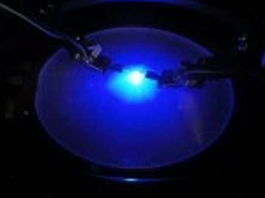
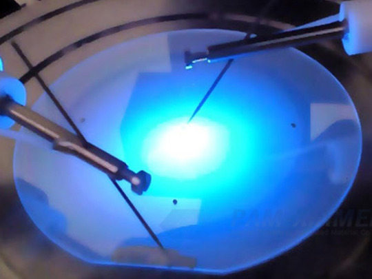
C-plane(0001) sapphire wafers are being extensively used for epitaxial growth of III-V and II-VI compounds, such as gallium nitride (GaN), aluminum nitride (AlN), for bright blue and green LED and laser diodes.
Technical Applications of Standard Sapphire Wafers
C-plane sapphire wafers are widely used to grow III-V and II-VI deposited films of wide band-gap nitride and oxide semiconductor materials such as gallium nitride (GaN), aluminum nitride (AlN), indium nitride (InN), zinc oxide (ZnO ultraviolet light emission) and tin oxide (SnO2 ultraviolet luminescent material), etc.
In addition, standard C-plane(0001) sapphire wafers are widely applied to fabricate LED white and blue light, ultraviolet and deep UV LED epitaxial wafers by Metal-Organic Vapor Deposition(MOCVD), Molecular Beam Epitaxy (MBE), Plasma Enhanced Chemical Vapor Deposition(PECVD) and other epitaxy growth methods.
CRYSCORE standard sapphire wafers also are used as the substrates of heterojunction bipolar transistor (HBT), a laser diode (LD), UV detector, nanotube, and the heat dissipation material of high temperature and high power high-frequency electronic device.
Competitive Advantages of CRYSCORE's Sapphire Wafers
99.999 % high purity single crystal Al2O3 material.
Special CMP (Chemical Mechanical Polishing) technology to ensure its performance at a low cost.
Excellent surface quality in all orientations (less than 0.2 nm for C-plane, less than 0.5 nm for A-plane, M-plane, R-plane, N-plane, V-plane, 10-14, etc.)
Cleaned in class 100 cleanroom by ultrapure water with quality above 18MΩ *cm.
25 pcs a pack or single pack is available to maximize customer flexibility in their research.
Traceable product serial number.
Compact carton packaging for safer shipping and cost-saving.
Standard wafers are Generally in stock to ensure a quick delivery.
As a professional sapphire wafer supplier, CRYSCORE aims to provide customers with the best products and services, and let our technology benefits the world.

0 notes
Link
마리화나 관련주 대장주 10종목 (핵심 종목 공유)
마리화나 관련주에 대해 알아보고자 합니다. 마리화나 관련주와 마리화나 대장주에 관련된 키워드로는 한국비엔씨 마이더스AI 우리바이오 코너스톤네트웍스 에이아이비트 에스엘바이오닉스 오성첨단소재 애머릿지 세미콘라이트 아이큐어 등이 있습니다.
아래에서 마리화나 관련주 및 마리화나 대장주에 대해 자세히 알아보겠습니다.
(adsbygoogle = window.adsbygoogle || []).push({});
# 현재 사이트 최고 인기 글
메타버스 관련주 바로가기
2차전지 관련주 바로가기
반도체 관련주 바로가기
우주항공 관련주 바로가기
드론택시(UAM) 관련주 바로가기
주식 카테고리 바로가기
우리바이오(082850) :: 마리화나 관련주
기업개요
(adsbygoogle = window.adsbygoogle || []).push({});
- 우리바이오는 2019년 신수종사업으로 헬스케어 산업을 선정하였으며, 첨단 광원 기술에 식물 재배 기술을 융합한 천연물 식물공장을 구축과 산학 협력 등 다양한 형태의 연구가 진행 중.
- 2,000평 규모의 GMP 인증 건강기능식품 제조 공장을 운영하고 있으며, 연질캡슐 등 첨단 제조시설 기반으로 B2B 시장에 진입하였음.
- 우리바이오는 헬스케어 사업의 다각화로 B2C 사업부 신설해 차별화된 건강기능식품을 고유 브랜드로 론칭하였고, 전국 약국 진입 예정.
실적 및 분석
- 우리바이오는 건강식품의 판매 호조에도 LED 및 BLU 부문의 부진으로 매출 규모는 전년대비 소폭 축소, 그러나 원가구조 개선되며 영업이익률 및 순이익률은 전년대비 상승.
- 누적 결손금 축소의 영향으로 제안정성 지표는 전년대비 개선되었으나, 여전히 자산대비 높은 부채부담을 보이고 있음.
- 우리바이오는 마이크로 및 미니 LED 시장의 확대로 외형 성장이 전망되며, 베타글루칸 독점 계약과 식의약품 원천소재 공동개발 등으로 중장기적 성장동력 확보도 기대됨.
마이더스AI(222810) :: 마리화나 관련주
기업개요
(adsbygoogle = window.adsbygoogle || []).push({});
- 마이더스ai는 기업용 보안 솔루션 관련 소프트웨어 개발을 주 사업으로 영위하고 있으며 엔드포인트 프로텍션 전문기업임.
- 2001년 PC보안제품 SafePC를 출시하였으며 개인정보보호, 보안USB, 네트워크접근제어 등의 엔드포인트 보안 제품을 지속적으로 개발하여 공급하고 있음.
- 마이더스ai는 에이전트 통합 보안 제품인 SafePCEnterprise 5.0를 출시하였으며 재해 복구 솔루션 및 모바일 정보유출통제 솔루션 등을 출시하며 라인업을 확대.
실적 및 분석
- 마이더스ai는 응용어플리케이션 SI 수주 호조에도 클라이언트보안 및 네트워크보안 솔루션 수주 부진으로 전년대비 매출규모 축소.
- 원가구조 개선에도 신규사업 초기 제비용 증가로 전년대비 영업손실 규모 확대, 이자비용 증가로 법인세비용 환급에도 순손실 규모 확대.
- 마이더스ai는 신규 사업으로 AI기술 기반의 한류콘텐츠를 서비스하는 통합포털과 블록체인 차량공유 플랫폼, ERP 기반의 IB 시스템 등을 출시할 예정인 바, 신성장동력 확보 기대.
한국비엔씨(256840) :: 마리화나 관련주
기업개요
(adsbygoogle = window.adsbygoogle || []).push({});
- 한국비엔씨는 2007년 8월 의료기기, 의약품, 건강보조식품 등의 개발, 제조, 판매 영위를 목적으로 설립되어 2019년 11월 엔에이치기업인수목적 11호와 합병으로 코스닥 시장에 상장함.
- 생체재료인 히알루론산, 콜라겐을 가공하여 의료기기, 의약품, 코스메슈티컬 제품 등 전략적 응용제품을 연구, 개발하여 HA필러, 유착방지재, 콜라겐흡수성창상피복재 등을 생산.
- 한국비엔씨는 2020년 식약처로부터 보톡스 수출허가를 받은 가운데 국내 시장에서 임상 1,2상 진행 중이며 연내 3상 진입도 예정되어 있음.
실적 및 분석
- 한국비엔씨는 COVID-19 영향에도 국내 및 러시아향 미용성형용제품권의 매출 증가와 수술/시술용제품군 호조로 상품 매출 부진에도 외형은 전년대비 신장.
- 신규제품 개발에 따른 연구개발비용과 인력 충원으로 인건비성 비용 증가에 따라 전년대비 영업이익률은 하락하였으나 전년도 합병상장비용 및 소송충당부채전입액 제거로 순이익 흑자전환.
- 한국비엔씨는 주력제품군인 필러제품군의 내수시장 경쟁 심화에도 창상피복재 및 조직보충재 등의 경쟁력을 기반으로 외형 성장 및 영업수익성 상승 기대.
아이큐어(175250) :: 마리화나 관련주
기업개요
(adsbygoogle = window.adsbygoogle || []).push({});
- 2000년 5월 설립되어, 약물전달시스템에 관한 원천기술을 바탕으로 패취형 의약품 중심의 의약품연구개발 및 의약품과 화장품 OEM, ODM 사업 영위.
- 주요 종속기업으로는 건강기능식품제조업체 (주)바이오로제트, 아이콰(상해)국제유한공사가 있으며 일반의약품 판매사인 (주)아이큐어비앤피 등이 있음.
- 2020년 결산 기준, 전문의약품 87품목, 일반의약품 50품목의 총 137품목 의약품과 총 15개 의약외품의 MFDS 허가 품목을 보유하고 있음.
실적 및 분석
- COVID-19에 따른 화장품 OEM 및 ODM 부문 부진에도 패취형 의약품 중심의 제약사업부문 제품 매출이 큰 폭으로 확대된바 전년대비 양호한 성장을 보임.
- 제품 원가 확대와 지급수수료 및 경상연구개발비 등 판관비 부담으로 영업적자 폭은 전년대비 확대되었으며 금융수지 개선과 대규모 종속기업투자주식처분이익에도 순손실 확대.
- 화장품 부문의 매출 회복과 붙이는 치매 치료제의 상반기 내 미국 FDA임상 신청 및 연내 생산이 시작될 예정인바 외형 성장 및 수익성 또한 점진적으로 개선될 전망.
세미콘라이트(214310) :: 마리화나 관련주
기업개요
(adsbygoogle = window.adsbygoogle || []).push({});
- 동사는 LED EPI wafer 및 Chip 설계, 개발, 생산 및 판매를 주요 사업 목적으로 2007년 7월에 설립되었음.
- 초소형 반도체 소자의 하나인 Flip-chip 기술을 기반으로 한 LED 칩을 개발하며, 주요 제품은 TV 백라이트유닛(BLU)용 LED칩과 조명용 LED 칩이 있음.
- 세계적으로 유일하게 Flip-chip LED의 반사층 관련 기술 특허를 보유하고 있는바, 독보적인 기술력 확보하고 있음.
실적 및 분석
- COVID-19 영향 및 글로벌 경기침체에도 주요 고객사인 루멘스향 공급물량이 확대됨에 따라 매출은 전년대비 증가하였음.
- 원가 및 판관비 부담 완화되며 영업손실 규모 전년대비 축소, 관계기업투자주식처분이 발생 및 금융자산평가손실 감소 등으로 순손실 규모도 축소.
- 주요 고객사의 미니 및 마이크로 LED 관련 사업 확대, 중국 화찬세미텍과의 라이선스 계약 체결, UV LED사업 강화 등으로 외형 성장 지속될 듯.
애머릿지(900100) :: 마리화나 관련주
기업개요
(adsbygoogle = window.adsbygoogle || []).push({});
- 뉴프라이드는 1978년 유제품 유통업을 목적으로 설립되어 현재는 인터모달(복합운송) 토털서비스(수리 및 정비, 관리용역) 제공업 및 수입차 판매업 등을 주력사업으로 영위함.
- 인터모달 지원 서비스를 제공하며 차량과 장비의 수리 및 정비 용역을 제공하는 미국법인과 화장품 도소매업 및 면세점 운영사업, 신규사업 등을 목적으로 한 종속기업들을 보유.
- 뉴프라이드는 인터모달 서비스는 철도 운송을 중심으로 컨테이너 선박과 트레일러 트럭 간에 화물을 환적할 때 이용되는 차량 및 그 장비에 대한 운용 및 관리서비스를 제공하는 것임.
실적 및 분석
- 뉴프라이드는 카나비스의 상품 매출 발생에도 신/재생 타이어의 매출이 급감한 가운데 기존 일부 상품 매출 제거에 따라 외형은 전년동기대비 큰 폭으로 축소되었음.
- 타이어부문의 강도 높은 구조조정으로 원가 및 판관비가 감소한바 전년동기대비 영업적자 폭은 축소되었으며 이자비용 및 투자자산처분손실 반영에도 순손실 또한 축소.
- 뉴프라이드는 미국 현지에서 마리화나 재배 공장 인수를 추진, 연내 본격적인 생산 예상되는 가운데 타이어사업부문의 구조조정으로 외형 및 수익 개선이 기대됨.
오성첨단소재(052420) :: 마리화나 관련주
기업개요
(adsbygoogle = window.adsbygoogle || []).push({});
- 오성첨단소재는 반도체 및 LCD 제조 장비, 환경시험 Tester 등의 제조를 목적으로 설립, 2018년 2월 장비사업부문 분할 후 현 상호로 변경하였으며 디스플레이용 소재를 생산하고 있음.
- 주요 제품은 디스플레이 FPD 기능성 광학 필름으로, 삼성 SDI 등 국내외 디스플레이 업체에 공급하고 있으며, 내수와 수출을 통해 판매하고 있음.
- 오성첨딘소재는 2018년 1월 사업다각화를 위해 카나비스메디칼을 설립, 자회사로 보유하고 있는 가운데 2019년 5월에는 2030청년주택사업을 영위하는 더블라썸묵동을 인수하였음.
실적 및 분석
- 오성첨단소재는 비산방지용, FPCB용 내열 등 복합소재 기능성 필름의 판매 감소에도 모바일, 노트북 등 편광판용 보호필름의 판매 증가, 임가공 코팅의 판매 호조로 전년대비 매출 성장.
- 매출 성장으로 원가구조 개선된 가운데 지급수수료 감소로 판관비 부담 완화되며 전년대비 영업이익률 상승, 그러나 외화 관련 영업외수지 저하, 법인세비용 발생으로 순이익률은 하락.
- 오성첨단소재는 글로벌 경기 개선으로 반도체 산업의 호조가 예상되는 가운데 보호필름의 수요가 증가하며 매출 성장 전망. 가동률 상승으로 영업이익률 상승세 이어갈 듯.
에스엘바이오닉스(214310) :: 마리화나 관련주
기업개요
(adsbygoogle = window.adsbygoogle || []).push({});
- 에스엘바이오닉스는 LED EPI wafer 및 Chip 설계, 개발, 생산 및 판매를 주요 사업 목적으로 2007년 7월에 설립되었음.
- 초소형 반도체 소자의 하나인 Flip-chip 기술을 기반으로 한 LED 칩을 개발하며, 주요 제품은 TV 백라이트유닛(BLU)용 LED칩과 조명용 LED 칩이 있음.
- 에스엘바이오닉스는 세계적으로 유일하게 Flip-chip LED의 반사층 관련 기술 특허를 보유하고 있는바, 독보적인 기술력 확보하고 있음.
실적 및 분석
- 에스엘바이오닉스는 COVID-19 영향 및 글로벌 경기침체에도 주요 고객사인 루멘스향 공급물량이 확대됨에 따라 매출은 전년대비 증가하였음.
- 원가 및 판관비 부담 완화되며 영업손실 규모 전년대비 축소, 관계기업투자주식처분이 발생 및 금융자산평가손실 감소 등으로 순손실 규모도 축소.
- 에스엘바이오닉스는 주요 고객사의 미니 및 마이크로 LED 관련 사업 확대, 중국 화찬세미텍과의 라이선스 계약 체결, UV LED사업 강화 등으로 외형 성장 지속될 듯.
에이아이비트(039230) :: 마리화나 관련주
기업개요
(adsbygoogle = window.adsbygoogle || []).push({});
- 에이아이비트는 LCD검사장비 및 관련 장치의 제조 및 판매업을 영위하며 종속회사인 Foxbrain HK Limited.는 중국, 대만 등 해외 마케팅 및 고객 서비스를 제공함.
- 전문성 제고와 경영효율성 강화를 위해 2017년 3월 디스플레이 패널을 검사하는 장비부문을 물적분할하여 자회사인 폭스디스플레이(주)를 신설함.
- 에이아이비트는 주요 제품은 Probe Unit(LCD 화상 점등검사장치)와 Probe Station(LCD 화상 점등 자동 검사장비), Laser MIicro-Processin 등이 있음.
실적 및 분석
- 에이아이비트는 신규 자회사 유파마디자인의 매출 기여에도 전방 디스플레이 산업의 부진으로 관련 LCD검사장비의 공급물량도 감소한바 외형은 전년대비 크게 축소.
- 원가구조 개선되며 영업이익률 전년대비 상승, 그러나 이자비용 증가 및 금융자산관련 손실 발생 등으로 순손실 규모는 전년대비 확대.
- 에이아이비트는 국내 LCD 디스플레이 시장이 위축되고 있으나 중국 C&W와의 대규모 검사장비 공급계약 체결, 바이오 사업 확대 등을 통해 외형 회복 가능할 듯.
코너스톤네트웍스(033110) :: 마리화나 관련주
기업개요
(adsbygoogle = window.adsbygoogle || []).push({});
- 코너스톤네트웍스는 1986년 4월에 설립되어 전자교육장비 및 전자계측기의 제조 및 유통업, 지능형 로봇의 개발과 제조 및 유통업을 주력사업으로 영위함.
- AWG(Arrrayed
- Waveguide Grating, 파장분할다중화기), ROADM, Optical Switch, Tranceiver 등 통신장비 신규 제품을 개발 중임.
- 코너스톤네트웍스는 창업투자회사인 티씨투자조합1호, 통신장비 제조업체인 (주)휘라포토닉스와 (주)티디아이 등을 종속기업으로 보유하고 있음.
실적 및 분석
- 코너스톤네트웍스는 주력인 전자교육장비의 판매가 위축되었으나 광통신부품 자회사들의 성장 등에 힘입어 매출 규모는 전년대비 크게 확대.
- 원가구조 악화와 대손상각비 등 판관비 증가로 영업손실 규모 전년대비 확대, 중단영업손실 제거에도 파생상품관련 수지 저하되며 순손실 규모 크게 확대.
- 코너스톤네트웍스는 5G 관련 광융합사업 추진이 기대되나 코로나19의 확산에 따른 수주 지연 등으로 매출 성장폭은 축소될 듯. 한편, 부분자본잠식상태가 지속되고 있는바 재무개선 노력 요구됨.
# 현재 사이트 최고 인기 글
메타버스 관련주 바로가기
2차전지 관련주 바로가기
반도체 관련주 바로가기
우주항공 관련주 바로가기
드론택시(UAM) 관련주 바로가기
주식 카테고리 바로가기
0 notes
Text
Epi Wafer Even After COVID-19 the Market Is Attractive
Latest released the research study on Global Epi Wafer Market, offers a detailed overview of the factors influencing the global business scope. Epi Wafer Market research report shows the latest market insights with upcoming trends and breakdown of the products and services. The report provides key statistics on the market status, size, share, growth factors of the Epi Wafer.
The study covers emerging player’s data, including: competitive situation, sales, revenue and global market share of top manufacturers are Siltronic AG (Germany),IQE PLC (United Kingdom),II-VI Incorporated (United States),SOITEC (France),GlobalWafers (United States),EpiGaN NV (Belgium),JENOPTIK Optical Systems (United States),Silicon Valley Microelectronics, Inc. (United States),SHOWA DENKO K.K (Japan),Nichia Corporation (Japan),Xiamen Powerway Advanced Material Co., Ltd. (China).
Free Sample Report + All Related Graphs & Charts @ : https://www.advancemarketanalytics.com/sample-report/6655-global-epi-wafer-market
Keep yourself up-to-date with latest market trends and changing dynamics due to COVID Impact and Economic Slowdown globally. Maintain a competitive edge by sizing up with available business opportunity in Global Epi Wafer Market various segments and emerging territory.
Epi Wafer Market Overview
Epi wafers are used in the production of semiconductors used in advanced devices. There is an epitaxial process which is the deposition of silicon or other substrate layers on the conductor. These epi wafer layers are provided on wireless, photonic and other power systems for providing better electrical performance. These are generally found in optical components, high-speed systems and now their applicational is enhanced to virtual technology gadgets and devices.
Market Drivers
The Demand for LED Light Application is Increasing in Various Industries
Growing Advanced Technology in Automotive Sector Because of Chemical and Physical Properties of Epitaxial Layer
Market Trend
The increasing use of semiconductors with silicon epi wafers in big data, 5G connectivity, energy reduction, electrification, and artificial intelligence. There are continuous research and development leading to technological innovations for various new a
Restraints
Higher Cost and Additional Complexities Involved with Epi Wafer Technology
Stringent Regulatory Compliance Regarding Epi wafer Technology
Challenges
The Defects Associated with Epi Layer
The Global Epi Wafer Market segments and Market Data Break Down are illuminated below:
by Application (Optical Components, Wireless Devices, Highspeed Systems, Photonic Products, Others), Material (Gallium Nitride (GaN), Silicon Carbide (SiC), Gallium Arsenide (GaAs)), Diameter (150mm, 200mm, 300mm)
Region Included are: North America, Europe, Asia Pacific, Oceania, South America, Middle East & Africa
Country Level Break-Up: United States, Canada, Mexico, Brazil, Argentina, Colombia, Chile, South Africa, Nigeria, Tunisia, Morocco, Germany, United Kingdom (UK), the Netherlands, Spain, Italy, Belgium, Austria, Turkey, Russia, France, Poland, Israel, United Arab Emirates, Qatar, Saudi Arabia, China, Japan, Taiwan, South Korea, Singapore, India, Australia and New Zealand etc.
Enquire for customization in Report @: https://www.advancemarketanalytics.com/enquiry-before-buy/6655-global-epi-wafer-market
Strategic Points Covered in Table of Content of Global Epi Wafer Market:
Chapter 1: Introduction, market driving force product Objective of Study and Research Scope the Epi Wafer market
Chapter 2: Exclusive Summary – the basic information of the Epi Wafer Market.
Chapter 3: Displaying the Market Dynamics- Drivers, Trends and Challenges & Opportunities of the Epi Wafer
Chapter 4: Presenting the Epi Wafer Market Factor Analysis, Post COVID Impact Analysis, Porters Five Forces, Supply/Value Chain, PESTEL analysis, Market Entropy, Patent/Trademark Analysis.
Chapter 5: Displaying the by Type, End User and Region/Country 2015-2020
Chapter 6: Evaluating the leading manufacturers of the Epi Wafer market which consists of its Competitive Landscape, Peer Group Analysis, BCG Matrix & Company Profile
Chapter 7: To evaluate the market by segments, by countries and by Manufacturers/Company with revenue share and sales by key countries in these various regions (2021-2026)
Chapter 8 & 9: Displaying the Appendix, Methodology and Data Source
Finally, Epi Wafer Market is a valuable source of guidance for individuals and companies in their decision framework.
Data Sources & Methodology
The primary sources involves the industry experts from the Global Epi Wafer Market including the management organizations, processing organizations, analytics service providers of the industry’s value chain. All primary sources were interviewed to gather and authenticate qualitative & quantitative information and determine the future prospects.
In the extensive primary research process undertaken for this study, the primary sources – Postal Surveys, telephone, Online & Face-to-Face Survey were considered to obtain and verify both qualitative and quantitative aspects of this research study. When it comes to secondary sources Company's Annual reports, press Releases, Websites, Investor Presentation, Conference Call transcripts, Webinar, Journals, Regulators, National Customs and Industry Associations were given primary weight-age.
For Early Buyers | Get Up to 20% Discount on This Premium Report: https://www.advancemarketanalytics.com/request-discount/6655-global-epi-wafer-market
What benefits does AMA research studies provides?
· Latest industry influencing trends and development scenario
· Open up New Markets
· To Seize powerful market opportunities
· Key decision in planning and to further expand market share
· Identify Key Business Segments, Market proposition & Gap Analysis
· Assisting in allocating marketing investments
Definitively, this report will give you an unmistakable perspective on every single reality of the market without a need to allude to some other research report or an information source. Our report will give all of you the realities about the past, present, and eventual fate of the concerned Market.
Thanks for reading this article; you can also get individual chapter wise section or region wise report version like North America, Europe or Asia.
About Author:
Advance Market Analytics is Global leaders of Market Research Industry provides the quantified B2B research to Fortune 500 companies on high growth emerging opportunities which will impact more than 80% of worldwide companies' revenues.
Our Analyst is tracking high growth study with detailed statistical and in-depth analysis of market trends & dynamics that provide a complete overview of the industry. We follow an extensive research methodology coupled with critical insights related industry factors and market forces to generate the best value for our clients. We Provides reliable primary and secondary data sources, our analysts and consultants derive informative and usable data suited for our clients business needs. The research study enable clients to meet varied market objectives a from global footprint expansion to supply chain optimization and from competitor profiling to M&As.
Contact Us:
Craig Francis (PR & Marketing Manager)
AMA Research & Media LLP
Unit No. 429, Parsonage Road Edison, NJ
New Jersey USA – 08837
Phone: +1 (206) 317 1218
Connect with us at
https://www.linkedin.com/company/advance-market-analytics
https://www.facebook.com/AMA-Research-Media-LLP-344722399585916
https://twitter.com/amareport
0 notes
Text
Use of Wafer Front End in the Semiconductor Manufacturing Process
When the process of front-end production is completed then to save the chip the wafers are transmitted to the assembly facility. It brings the heat from the devices, assists the integration into the electronic systems, and confines the electric interference.
Building of wafers
In manufacturing, the semiconductor has an essential role no matter whether it is a small chip or a big motor car. In semiconductor production, the processing of chemical elements is done in the wafer form. Within the plastic cassettes, the LED Epi wafer is built up and with the specific production time, the circumstances are made out of steps.
Wafer handling equipment is the emerging manufacturing process that is made to check the cleanliness and environmental control. Within the semiconductor front-end industry, it has diminished from the semiconductor devices manufacturing. For the significant environments, the process is carried out where certain factors are checked out, such as humidity, particle contamination, temperature, and controlled with the particular parameters.
To handle delicate thin wafers the bonding of the device wafer is done with a rigid carrier substrate before the back-thinning process. With the use of an adhesive bonding layer, the originally thick device wafer is bonded with its active surface to a carrier wafer.
It arrives in a consignment production form if we discuss the semiconductor backend production that is based on many customers' various orders. Picked up from the GaN LED wafers conveyed from the front-end production, the backend companies with the non-defective dies start building the final product in such a case. It makes the products reach their place within the due dates.

LED epitaxial wafer gives a detailed description of the non-repairable chips that are pushed to the next step. The defectiveness and the opposed information are filled up when this test gets completed and based on the matter it is passed through the backend process. The information conveys that only non-defective dies are taken in the final product. Wafer handling equipment is the emerging manufacturing process that is made to check the cleanliness and environmental control. Within the semiconductor front-end industry, it has diminished from the semiconductor devices manufacturing. The manufacturers, as with the bump in the semiconductor's request, turn on a further note towards automating the production process.
Original source: https://ganwafer.weeblysite.com/
3 notes
·
View notes
Quote
We provide four different crystal structure of silicon carbide (SiC) crystal. Namely they are 6H-SiC Wurtzite ( Hexagonal), 4H-SiC Wurtzite ( Hexagonal), 3C-SiC Zinc blende (cubic) and SiC Epi wafer. It is widely used LED, RF, high power devices, high temperature devices and high frequency power devices manufacturing industries to produce quality semiconductor products.
Qualitymaterial
0 notes
Text
LED Epi wafer Market 2019 Global Trend, Growth, Demand, Size, Segmentation and Opportunities Forecast To 2025
LED Epi wafer Market 2019 Global Trend, Growth, Demand, Size, Segmentation and Opportunities Forecast To 2025
Access the PDF sample of the report @ https://www.orbisresearch.com/contacts/request-sample/3572769
In this report, we provide assessment of market definition along with the identification of key players and an analysis of their Production?Revenue?Price?Cost and Gross Margin their SWOT analysis for this market during the forecast period. Quantitative analysis of the industry from 2014 to 2025 by…
View On WordPress
#LED Epi wafer market#LED Epi wafer market analysis#LED Epi wafer market forecast#LED Epi wafer market growth#LED Epi wafer market overview#LED Epi wafer market research#LED Epi wafer market share#LED Epi wafer market size#LED Epi wafer market study
0 notes
Text
Silicon EPI Wafer Market: Global Industry Growth, Market Size, Market Share and Forecast 2020-2027
According to the recent report published by Research Corridor, the Global Silicon EPI Wafer Market is expected to provide sustainable growth opportunities during the forecast period from 2020 to 2027. This latest industry research study analyzes the Silicon EPI Wafer market by various product segments, applications, regions and countries while assessing regional performances of numerous leading market participants.
The report titled "Silicon EPI Wafer Market - Global Trends, Market Share, Industry Size, Growth, Opportunities, and Forecast - 2020 – 2027" offers a holistic view of the Silicon EPI Wafer industry encompassing numerous stakeholders including raw material suppliers, providers, distributors, consumers and government agencies, among others. Furthermore, the report includes detailed quantitative and qualitative analysis of the global Silicon EPI Wafer market considering market history, product development, regional dynamics, competitive landscape, and key success factors (KSFs) in the industry.
Browse Full report on Global Silicon EPI Wafer Market report at https://www.researchcorridor.com/silicon-epi-wafer-market/
The report includes a deep-dive analysis of key countries including the U.S., Canada, the U.K., Germany, France, China, Japan, India, Australia, Mexico, Brazil and South Africa, among others. Thereby, the report identifies unique growth opportunities across the world based on trends occurring in various developed and developing economies.
Silicon EPI Wafer Market report summarizes the positive growth rate in upcoming years, and market size with competitive analysis. Our experts have analyzed the historical data to compare with the current market scenario to calculate the market growth in the coming years. The study provides an exhaustive report that includes an executive summary, scope, and forecast of the market.
The Silicon EPI Wafer Market Segmentation:
By Type
Heteroepitaxy
Homoepitaxy
By Wafer Size
6-inch
8-inch
12-inch
Others
By Application
LED
Power Semiconductor
MEMS-based Devices
By Industry Vertical
Consumer Electronics
Automotive
Healthcare
Industrial
Others
By Region:
· North America
· Europe
· Asia Pacific
· Latin America
· Middle East & Africa
To know more about the study, make an inquiry before purchase @ https://www.researchcorridor.com/inquiry/?id=143929
List of Key companies:
Nichia Corporation
Applied Materials
Sumco Corporation
Epigan
ASM
Global Wafers
Siltronic
Wafer World Inc.
Key Questions Answered by Silicon EPI Wafer Market Report
Product popularity and adoption based on various country-level dynamics
Regional presence and product development for leading market participants
Market forecasts and trend analysis based on ongoing investments and economic growth in key countries
Competitive landscape based on revenue, product offerings, years of presence, number of employees and market concentration, among others
number of employees and market concentration, among others
To know more about this study, request a free sample report @ https://www.researchcorridor.com/request-sample/?id=143929
About Us:
Research Corridor is a global market research firm. Our insightful analysis is focused on developed and emerging markets. We identify trends and forecast markets with a view to aid businesses identify market opportunities optimize strategies. Our expert’s team of analysts’ provides enterprises with strategic insights. Research Corridor works to help enterprises grow through strategic insights and actionable solutions. Feel free to contact us for any report customization at [email protected] .
Media Contact:
Company Name: Research Corridor
Contact Person: Mr. Vijendra Singh
Email: [email protected]
Contact no: +91 989-368-5690
Visit us:
https://www.researchcorridor.com/
0 notes
Text
Epitaxial Wafer Market Drivers, Opportunities, Industry Analysis and Forecast till 2026
Summary:
Epitaxial Wafer, also known as Epi-wafer is placed over other silicon wafer through epitaxial process. Epitaxy is a process in which a monocrystalline silicon layer is deposited over the polished crystal surface of a silicon wafer. This wafer acts as semiconducting substrate for applications such as microelectronics, photovoltaic, and photonics. There are two types of epitaxial wafer named; Homoepitaxy and Heteroepitaxy.
Key Driver:
Major factor driving growth of the Epitaxial Wafer Market is increasing use of LED lighting across the globe and this is fueling demand for epitaxial wafer. For instance, according to Coherent Market Insights’ analysis, the rate of LED lighting penetration in 2015 was 15% and it has increased to 27% in 2016, globally.
The factor attributed to growth of LED lighting is increasing demand for energy efficient lighting products that help in reducing consumption of electricity and this is a major factor for replacing conventional lighting products with LED lighting across residential, commercial, and industrial sectors.
LED lights are mainly incorporated with number of ICs. These ICs are manufactured from silicon wafer chip as silicon wafer. Thus, in order to increase the performance of silicon wafer, the manufacturer coats this silicon wafer with epitaxial layer. This growth of epitaxial layer over silicon wafer helps in increasing electrical characteristic of the wafer, which in turn increases the power capability of LED lighting.
Increasing silicon wafer shipments is further driving growth of the market. For instance, according to SEMI, total silicon wafer area shipments reached 3,255 million square inches during the third quarter of 2018, a 3.0% rise from the 3,164 million square inches shipped during the second quarter of 2018.
Request for the sample copy @ https://www.coherentmarketinsights.com/insight/request-sample/2277
Key Restraint
Initial high capital investments will restrict small players to enter in the semiconductor manufacturing sector.
Statistics:
The market for epitaxial wafer in Asia Pacific accounted for largest share in the global market in 2017.
Request for the PDF Brochure @ https://www.coherentmarketinsights.com/insight/request-pdf/2277
Key Opportunities:
The factor attributed to growth of this market is increasing penetration of smartphones, increasing adoption of IoT, self-driving cars, and others. For instance, according to the Coherent Market Insights’ analysis, the number of smartphone users in India was 292.6 million in 2016 and it has grown to 342 million in 2017.
Increasing demand for smartphones and advancement in smartphone technology has led to development of thinner and smaller ICs. Hence, growing demand for these electronic products is driving manufacturers to coat this wafer with epitaxial wafer that further increase the power of these electronic devices.
Moreover, presence of key manufacturers such as Samsung, Sony, LG, Toshiba, Panasonic, Toyota, and Honda makes this region largest consumer of semiconductor ICs. The presence of players accelerates manufacturing of ICs. Hence, this will be another factor resulting in increasing demand for epitaxial wafer in this particular region.
Major players operating in the global Epitaxial Wafer Market include:
EpiWorks Inc., Global Wafers Japan Co. Ltd., Nichia Corporation, SHOWA DENKO K.K., Siltronic AG, Desert Silicon Inc., Electronics and Materials Corporation Ltd. Intelligent Epitaxy Technology Inc.IQE plc. , Jenoptic AG, MOSPEC Semiconductor Corporation, Norstel AB, Ommic S.A., Silicon Valley Microelectronics Inc. ,SVT Associates Inc. Universal Wafer Inc., Wafer Works Corporation, Xiamen Powerway Advanced Materials Co. Ltd., and Visual Photonics Epitaxy Co. Ltd.
About Us
Coherent Market Insights is a global market intelligence and consulting organization focused on assisting our plethora of clients achieve transformational growth by helping them make critical business decisions.
What we provide:
Customized Market Research Services
Industry Analysis Services
Business Consulting Services
Market Intelligence Services
Long term Engagement Model
Country Specific Analysis
Contact Us:
Mr. Shah
Coherent Market Insights Pvt.Ltd.
Address: 1001 4th Ave, #3200 Seattle, WA 98154, U.S.
Phone: +1–206–701–6702
Email: [email protected]
#epitaxial wafer market#coherent market insights#market research#market analysis#business consulting
0 notes
Text
GaN Epitaxial Wafers Market Analysis, Top Manufacturers, Share, Growth, Opportunities and Forecast To 2027
Market Overview
An epitaxial wafer also known as, epi wafer, is a wafer of semiconducting material made by epitaxial growth (epitaxy) for use in photonics, microelectronics, spintronics, or photovoltaic. The epitaxial layers consist of various compounds such as gallium nitride (GaN), gallium arsenide (GaAs), or some combination of the element’s gallium, indium, aluminum, nitrogen, phosphorus or arsenic. High electron mobility, low switching losses, and fewer lattice mismatches are some of the key advantages of GaN Substrate, which are leading its adoption in industries such as power electronics and optoelectronics.
Furthermore, GaN epitaxial wafers are developed by hydride vapor-phase epitaxy (HVPE) or metal organic chemical vapor phase deposition (MOCVD) method, and can be used as an ideal and excellent substrate for high frequency, high speed, and high-power devices. The GaN epitaxial wafers are developed by several firms such as Aixtron, EpiGaN nv, Sciocs, and Semiconductor Wafer Inc.
Request Sample Copy Of This Business Report: https://www.coherentmarketinsights.com/insight/request-sample/3219
Market Dynamics
GaN is widely implemented in radio frequency devices, light-emitting diodes (LEDs), and power electronics, due to its ability to operate at high frequency and high temperature. Increasing adoption of LEDs is a major factor boosting growth of the GaN epitaxial wafers market. Furthermore, advancement in GaN technology has led to the development of efficient GaN substrates with free macro defect density and low defect density. Hence, GaN substrates can increasingly be used for realizing LEDs with a wafer diameter from 2 inch up to 6 and 8 inches. Increasing adoption of LEDs is expected to drive growth of the GaN epitaxial wafers market during the forecast period. However, competition from Sic in high-voltage semiconductor applications and high product cost are factors which are expected to hinder growth of the global GaN epitaxial wafers market during the forecast period.
In terms of geography, Asia Pacific is expected to be dominant in the global GaN epitaxial wafers market during the forecast period. This is owing to wide utilization of GaN-based transistors in the defense and military sector, increasing demand for LEDs from various industries such as consumer electronics & automotive and increasing renewable energy generation in the region. For instance, in June 2019, Samsung announced the launch of The Wall Luxury GaN micro-LED display configurable from 73” in 2K to 292” in 8K. Moreover, Asia Pacific region is expected to witness significant growth over the forecast period, which can be attributed to high adoption of innovative technologies such as epi-nucleation, buffer structure technology etc. in countries such as China, Japan, South Korea, and India. Key players in this region are focused on offering new products in order to meet increasing needs and requirements of consumers. For instance, in June 2019, Xiamen San'an Integrated Circuit Co., Ltd., a China-based pure-play wafer foundry with its advanced compound semiconductor technology platform, announced the launch of its 150mm gallium nitride (GaN) on silicon wafer foundry services, which is intended for the latest high voltage DC/AC and AC/DC power electronics applications worldwide.
Get Request Customization Copy Of This Business Report: https://www.coherentmarketinsights.com/insight/request-customization/3219
Key players in the global GaN epitaxial wafers market are RF Globalnet, Aixtron, EpiGaN nv, Sciocs, Semiconductor Wafer Inc. IGSS GaN, SweGaN, NTT Advanced Technology Corporation, Infineon Technologies AG, Mitsubishi Electric Corporation, Toshiba Infrastructure Systems & Solutions Corporation, Koninklijke Philips N.V., and ALLOS Semiconductors GmbH among others.
About Coherent Market Insights:
Coherent Market Insights is a prominent market research and consulting firm offering action-ready syndicated research reports, custom market analysis, consulting services, and competitive analysis through various recommendations related to emerging market trends, technologies, and potential absolute dollar opportunity.
Contact Us:
Name: Mr. Raj Shah
Phone: US +12067016702 / UK +4402081334027
Email: [email protected]
Visit Our Blogs: https://blog.coherentmarketinsights.com
0 notes
Text
STANDARD SAPPHIRE WAFERS (C-PLANE)
https://www.cryscor.com/products/standard-sapphire-wafers/

CRYSCORE can offer Epi-Ready grade sapphire wafer with a very low surface roughness in complete orientation options.
C-plane(0001) sapphire wafers are being extensively used for epitaxial growth of III-V and II-VI compounds, such as gallium nitride (GaN), aluminum nitride (AlN), for bright blue and green LED and laser diodes.
Technical Applications of Standard Sapphire Wafers
C-plane sapphire wafers are widely used to grow III-V and II-VI deposited films of wide band-gap nitride and oxide semiconductor materials such as gallium nitride (GaN), aluminum nitride (AlN), indium nitride (InN), zinc oxide (ZnO ultraviolet light emission) and tin oxide (SnO2 ultraviolet luminescent material), etc.
In addition, standard C-plane(0001) sapphire wafers are widely applied to fabricate LED white and blue light, ultraviolet and deep UV LED epitaxial wafers by Metal-Organic Vapor Deposition(MOCVD), Molecular Beam Epitaxy (MBE), Plasma Enhanced Chemical Vapor Deposition(PECVD) and other epitaxy growth methods.
CRYSCORE standard sapphire wafers also are used as the substrates of heterojunction bipolar transistor (HBT), a laser diode (LD), UV detector, nanotube, and the heat dissipation material of high temperature and high power high-frequency electronic device.
Competitive Advantages of CRYSCORE's Sapphire Wafers
99.999 % high purity single crystal Al2O3 material.
Special CMP (Chemical Mechanical Polishing) technology to ensure its performance at a low cost.
Excellent surface quality in all orientations (less than 0.2 nm for C-plane, less than 0.5 nm for A-plane, M-plane, R-plane, N-plane, V-plane, 10-14, etc.)
Cleaned in class 100 cleanroom by ultrapure water with quality above 18MΩ *cm.
25 pcs a pack or single pack is available to maximize customer flexibility in their research.
Traceable product serial number.
Compact carton packaging for safer shipping and cost-saving.
Standard wafers are Generally in stock to ensure a quick delivery.
0 notes
Last Seen Blogs

ryaneckphotography
ryan eck photographies


ionlyeatcomfortfood
The Stardust Collective

a-feral-child-let-lose
brainrot posts

polaris-australis
got into grad school and all i got was existential