#led epi wafer manufacturer
Text
Use of Wafer Front End in the Semiconductor Manufacturing Process
When the process of front-end production is completed then to save the chip the wafers are transmitted to the assembly facility. It brings the heat from the devices, assists the integration into the electronic systems, and confines the electric interference.
Building of wafers
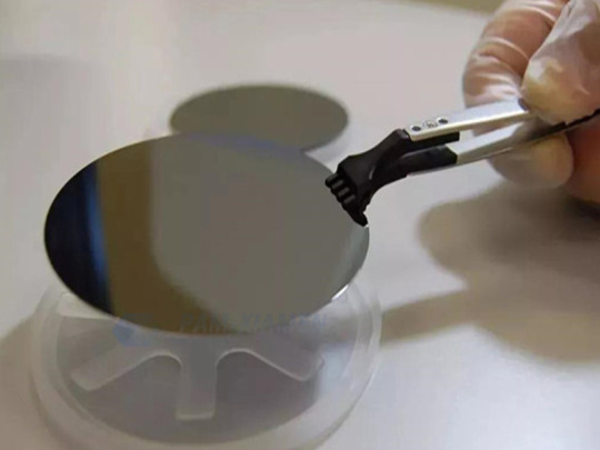
In manufacturing, the semiconductor has an essential role no matter whether it is a small chip or a big motor car. In semiconductor production, the processing of chemical elements is done in the wafer form. Within the plastic cassettes, the LED Epi wafer is built up and with the specific production time, the circumstances are made out of steps.
Wafer handling equipment is the emerging manufacturing process that is made to check the cleanliness and environmental control. Within the semiconductor front-end industry, it has diminished from the semiconductor devices manufacturing. For the significant environments, the process is carried out where certain factors are checked out, such as humidity, particle contamination, temperature, and controlled with the particular parameters.
To handle delicate thin wafers the bonding of the device wafer is done with a rigid carrier substrate before the back-thinning process. With the use of an adhesive bonding layer, the originally thick device wafer is bonded with its active surface to a carrier wafer.
It arrives in a consignment production form if we discuss the semiconductor backend production that is based on many customers' various orders. Picked up from the GaN LED wafers conveyed from the front-end production, the backend companies with the non-defective dies start building the final product in such a case. It makes the products reach their place within the due dates.

LED epitaxial wafer gives a detailed description of the non-repairable chips that are pushed to the next step. The defectiveness and the opposed information are filled up when this test gets completed and based on the matter it is passed through the backend process. The information conveys that only non-defective dies are taken in the final product. Wafer handling equipment is the emerging manufacturing process that is made to check the cleanliness and environmental control. Within the semiconductor front-end industry, it has diminished from the semiconductor devices manufacturing. The manufacturers, as with the bump in the semiconductor's request, turn on a further note towards automating the production process.
Original source: https://ganwafer.weeblysite.com/
3 notes
·
View notes
Text
Epi Wafer Even After COVID-19 the Market Is Attractive
Latest released the research study on Global Epi Wafer Market, offers a detailed overview of the factors influencing the global business scope. Epi Wafer Market research report shows the latest market insights with upcoming trends and breakdown of the products and services. The report provides key statistics on the market status, size, share, growth factors of the Epi Wafer.
The study covers emerging player’s data, including: competitive situation, sales, revenue and global market share of top manufacturers are Siltronic AG (Germany),IQE PLC (United Kingdom),II-VI Incorporated (United States),SOITEC (France),GlobalWafers (United States),EpiGaN NV (Belgium),JENOPTIK Optical Systems (United States),Silicon Valley Microelectronics, Inc. (United States),SHOWA DENKO K.K (Japan),Nichia Corporation (Japan),Xiamen Powerway Advanced Material Co., Ltd. (China).
Free Sample Report + All Related Graphs & Charts @ : https://www.advancemarketanalytics.com/sample-report/6655-global-epi-wafer-market
Keep yourself up-to-date with latest market trends and changing dynamics due to COVID Impact and Economic Slowdown globally. Maintain a competitive edge by sizing up with available business opportunity in Global Epi Wafer Market various segments and emerging territory.
Epi Wafer Market Overview
Epi wafers are used in the production of semiconductors used in advanced devices. There is an epitaxial process which is the deposition of silicon or other substrate layers on the conductor. These epi wafer layers are provided on wireless, photonic and other power systems for providing better electrical performance. These are generally found in optical components, high-speed systems and now their applicational is enhanced to virtual technology gadgets and devices.
Market Drivers
The Demand for LED Light Application is Increasing in Various Industries
Growing Advanced Technology in Automotive Sector Because of Chemical and Physical Properties of Epitaxial Layer
Market Trend
The increasing use of semiconductors with silicon epi wafers in big data, 5G connectivity, energy reduction, electrification, and artificial intelligence. There are continuous research and development leading to technological innovations for various new a
Restraints
Higher Cost and Additional Complexities Involved with Epi Wafer Technology
Stringent Regulatory Compliance Regarding Epi wafer Technology
Challenges
The Defects Associated with Epi Layer
The Global Epi Wafer Market segments and Market Data Break Down are illuminated below:
by Application (Optical Components, Wireless Devices, Highspeed Systems, Photonic Products, Others), Material (Gallium Nitride (GaN), Silicon Carbide (SiC), Gallium Arsenide (GaAs)), Diameter (150mm, 200mm, 300mm)
Region Included are: North America, Europe, Asia Pacific, Oceania, South America, Middle East & Africa
Country Level Break-Up: United States, Canada, Mexico, Brazil, Argentina, Colombia, Chile, South Africa, Nigeria, Tunisia, Morocco, Germany, United Kingdom (UK), the Netherlands, Spain, Italy, Belgium, Austria, Turkey, Russia, France, Poland, Israel, United Arab Emirates, Qatar, Saudi Arabia, China, Japan, Taiwan, South Korea, Singapore, India, Australia and New Zealand etc.
Enquire for customization in Report @: https://www.advancemarketanalytics.com/enquiry-before-buy/6655-global-epi-wafer-market
Strategic Points Covered in Table of Content of Global Epi Wafer Market:
Chapter 1: Introduction, market driving force product Objective of Study and Research Scope the Epi Wafer market
Chapter 2: Exclusive Summary – the basic information of the Epi Wafer Market.
Chapter 3: Displaying the Market Dynamics- Drivers, Trends and Challenges & Opportunities of the Epi Wafer
Chapter 4: Presenting the Epi Wafer Market Factor Analysis, Post COVID Impact Analysis, Porters Five Forces, Supply/Value Chain, PESTEL analysis, Market Entropy, Patent/Trademark Analysis.
Chapter 5: Displaying the by Type, End User and Region/Country 2015-2020
Chapter 6: Evaluating the leading manufacturers of the Epi Wafer market which consists of its Competitive Landscape, Peer Group Analysis, BCG Matrix & Company Profile
Chapter 7: To evaluate the market by segments, by countries and by Manufacturers/Company with revenue share and sales by key countries in these various regions (2021-2026)
Chapter 8 & 9: Displaying the Appendix, Methodology and Data Source
Finally, Epi Wafer Market is a valuable source of guidance for individuals and companies in their decision framework.
Data Sources & Methodology
The primary sources involves the industry experts from the Global Epi Wafer Market including the management organizations, processing organizations, analytics service providers of the industry’s value chain. All primary sources were interviewed to gather and authenticate qualitative & quantitative information and determine the future prospects.
In the extensive primary research process undertaken for this study, the primary sources – Postal Surveys, telephone, Online & Face-to-Face Survey were considered to obtain and verify both qualitative and quantitative aspects of this research study. When it comes to secondary sources Company's Annual reports, press Releases, Websites, Investor Presentation, Conference Call transcripts, Webinar, Journals, Regulators, National Customs and Industry Associations were given primary weight-age.
For Early Buyers | Get Up to 20% Discount on This Premium Report: https://www.advancemarketanalytics.com/request-discount/6655-global-epi-wafer-market
What benefits does AMA research studies provides?
· Latest industry influencing trends and development scenario
· Open up New Markets
· To Seize powerful market opportunities
· Key decision in planning and to further expand market share
· Identify Key Business Segments, Market proposition & Gap Analysis
· Assisting in allocating marketing investments
Definitively, this report will give you an unmistakable perspective on every single reality of the market without a need to allude to some other research report or an information source. Our report will give all of you the realities about the past, present, and eventual fate of the concerned Market.
Thanks for reading this article; you can also get individual chapter wise section or region wise report version like North America, Europe or Asia.
About Author:
Advance Market Analytics is Global leaders of Market Research Industry provides the quantified B2B research to Fortune 500 companies on high growth emerging opportunities which will impact more than 80% of worldwide companies' revenues.
Our Analyst is tracking high growth study with detailed statistical and in-depth analysis of market trends & dynamics that provide a complete overview of the industry. We follow an extensive research methodology coupled with critical insights related industry factors and market forces to generate the best value for our clients. We Provides reliable primary and secondary data sources, our analysts and consultants derive informative and usable data suited for our clients business needs. The research study enable clients to meet varied market objectives a from global footprint expansion to supply chain optimization and from competitor profiling to M&As.
Contact Us:
Craig Francis (PR & Marketing Manager)
AMA Research & Media LLP
Unit No. 429, Parsonage Road Edison, NJ
New Jersey USA – 08837
Phone: +1 (206) 317 1218
Connect with us at
https://www.linkedin.com/company/advance-market-analytics
https://www.facebook.com/AMA-Research-Media-LLP-344722399585916
https://twitter.com/amareport
0 notes
Quote
We provide four different crystal structure of silicon carbide (SiC) crystal. Namely they are 6H-SiC Wurtzite ( Hexagonal), 4H-SiC Wurtzite ( Hexagonal), 3C-SiC Zinc blende (cubic) and SiC Epi wafer. It is widely used LED, RF, high power devices, high temperature devices and high frequency power devices manufacturing industries to produce quality semiconductor products.
Qualitymaterial
0 notes
Text
SAPPHIRE WAFERS / SAPPHIRE SUBSTRATES
https://www.cryscor.com/products/sapphire-wafers-sapphire-substrates/

Due to the less mismatched lattice and stable chemical and physical properties, sapphire(Al2O3) wafer is the popular substrates for III-V nitrides, superconductor and magnetic epi-film. They are widely used in GaN and thin-film epitaxial growth, silicon on sapphire, LED market and optics industry.
CRYSCORE is a professional sapphire wafer supplier who manufactures 99.999% high purity single crystal polished sapphire wafers for epitaxy. And our sapphire (Al2O3) substrates feature excellent surface finish, which is the key LED parameter.
If you are looking for reliable sapphire wafer suppliers, contact us now.
FEATURES OF SINGLE CRYSTAL SAPPHIRE
1. Sapphire has a high optical transmittance, so it is widely used as microelectronic tube dielectric material, ultrasonic conduction element, waveguide laser cavity and other optical elements, as window materials for infrared military devices, space vehicles, high-intensity lasers and optical communications...
2. Sapphire has high rigidity, high strength, high working temperature, abrasion resistance, corrosion resistance characteristics, so it is often used in harsh environments, such as boiler water gauge (high-temperature resistance), commodity bar code scanner, bearing and other precision manufacturing (wear resistance), coal, gas, well detection sensors and detector windows (anti-corrosion)...
3. Sapphire has the characteristics of electrical insulation, transparency, good thermal conductivity and high rigidity, so it can be used as the substrate material of integrated circuits, such as LED and microelectronic circuits, ultra-high-speed integrated circuit.
CRYSCORE'S EXCELLENT SAPPHIRE WAFERS
99.999 % high purity single crystal Al2O3 material.
Special CMP (Chemical Mechanical Polishing) technology to ensure its performance at a low cost.
Excellent surface quality in all orientations (less than 0.2 nm for C-plane, less than 0.5 nm for A-plane, M-plane, R-plane, N-plane, V-plane, 10-14, etc.)
Cleaned in class 100 cleanroom by ultrapure water with quality above 18MΩ *cm.
25 pcs a pack or single pack is available to maximize customer flexibility in their research.
Traceable product serial number.
Compact carton packaging for safer shipping and cost-saving.
Standard wafers are Generally in stock to ensure a quick delivery.
LOOK AT WHERE SAPPHIRE WAFER APPLIED
1. Semiconductor LED industry (MOCVD epitaxial GaN substrate)
In general, C-plane sapphire is needed in this area. R-plane or M-plane mainly used to grow non-polar/semi-polar plane epitaxial layers to improve the luminescence efficiency.
2. The growth of III-V or II-VI compound semiconductor.
3. Microelectronic IC applications especially Very High-Speed Integrated Circuit, SOS
Generally, it is a silicon heteroepitaxial deposition on R-plane sapphire.
4. Hybrid microelectronics
Hybrid microelectronics products are mainly HIC and MCM. It has high requirements on the substrate, while sapphire's characteristics such as stable dielectric constant and low dielectric loss make sapphire wafer the most commonly used substrate for HIC and the main substrate for MCM. Generally, the A-plane sapphire wafer is needed.
SAPPHIRE WAFER PROCESSING
At the very beginning, we have a crystal boule.
Crystal growing: Produce high-quality sapphire monocrystals via furnace.
Sapphire ingot processing: Drill out the ingot, Ground the ingot, Quality inspection.
Then we get the sapphire ingot.
Orientation: Position the ingot on the sawing machine.
Sawing: Cut the ingot into thin wafers.
Lapping: Lap the wafer to remove the scratched layer and improve its flatness.
Chamfer: Trim the edge of the wafer into an arc to improve the mechanical strength, to avoiding stress concentration.
Polishing: Reduce the surface roughness to reach the epitaxial wafer grade.
Cleaning: Remove dirt from the wafer surface.
Quality inspection: Inspect wafer with a high precision instrument to meet customer's requests.
Finally, we get the sapphire wafer.
0 notes
Text
Epitaxial Wafer Market Drivers, Opportunities, Industry Analysis and Forecast till 2026
Summary:
Epitaxial Wafer, also known as Epi-wafer is placed over other silicon wafer through epitaxial process. Epitaxy is a process in which a monocrystalline silicon layer is deposited over the polished crystal surface of a silicon wafer. This wafer acts as semiconducting substrate for applications such as microelectronics, photovoltaic, and photonics. There are two types of epitaxial wafer named; Homoepitaxy and Heteroepitaxy.
Key Driver:
Major factor driving growth of the Epitaxial Wafer Market is increasing use of LED lighting across the globe and this is fueling demand for epitaxial wafer. For instance, according to Coherent Market Insights’ analysis, the rate of LED lighting penetration in 2015 was 15% and it has increased to 27% in 2016, globally.
The factor attributed to growth of LED lighting is increasing demand for energy efficient lighting products that help in reducing consumption of electricity and this is a major factor for replacing conventional lighting products with LED lighting across residential, commercial, and industrial sectors.
LED lights are mainly incorporated with number of ICs. These ICs are manufactured from silicon wafer chip as silicon wafer. Thus, in order to increase the performance of silicon wafer, the manufacturer coats this silicon wafer with epitaxial layer. This growth of epitaxial layer over silicon wafer helps in increasing electrical characteristic of the wafer, which in turn increases the power capability of LED lighting.
Increasing silicon wafer shipments is further driving growth of the market. For instance, according to SEMI, total silicon wafer area shipments reached 3,255 million square inches during the third quarter of 2018, a 3.0% rise from the 3,164 million square inches shipped during the second quarter of 2018.
Request for the sample copy @ https://www.coherentmarketinsights.com/insight/request-sample/2277
Key Restraint
Initial high capital investments will restrict small players to enter in the semiconductor manufacturing sector.
Statistics:
The market for epitaxial wafer in Asia Pacific accounted for largest share in the global market in 2017.
Request for the PDF Brochure @ https://www.coherentmarketinsights.com/insight/request-pdf/2277
Key Opportunities:
The factor attributed to growth of this market is increasing penetration of smartphones, increasing adoption of IoT, self-driving cars, and others. For instance, according to the Coherent Market Insights’ analysis, the number of smartphone users in India was 292.6 million in 2016 and it has grown to 342 million in 2017.
Increasing demand for smartphones and advancement in smartphone technology has led to development of thinner and smaller ICs. Hence, growing demand for these electronic products is driving manufacturers to coat this wafer with epitaxial wafer that further increase the power of these electronic devices.
Moreover, presence of key manufacturers such as Samsung, Sony, LG, Toshiba, Panasonic, Toyota, and Honda makes this region largest consumer of semiconductor ICs. The presence of players accelerates manufacturing of ICs. Hence, this will be another factor resulting in increasing demand for epitaxial wafer in this particular region.
Major players operating in the global Epitaxial Wafer Market include:
EpiWorks Inc., Global Wafers Japan Co. Ltd., Nichia Corporation, SHOWA DENKO K.K., Siltronic AG, Desert Silicon Inc., Electronics and Materials Corporation Ltd. Intelligent Epitaxy Technology Inc.IQE plc. , Jenoptic AG, MOSPEC Semiconductor Corporation, Norstel AB, Ommic S.A., Silicon Valley Microelectronics Inc. ,SVT Associates Inc. Universal Wafer Inc., Wafer Works Corporation, Xiamen Powerway Advanced Materials Co. Ltd., and Visual Photonics Epitaxy Co. Ltd.
About Us
Coherent Market Insights is a global market intelligence and consulting organization focused on assisting our plethora of clients achieve transformational growth by helping them make critical business decisions.
What we provide:
Customized Market Research Services
Industry Analysis Services
Business Consulting Services
Market Intelligence Services
Long term Engagement Model
Country Specific Analysis
Contact Us:
Mr. Shah
Coherent Market Insights Pvt.Ltd.
Address: 1001 4th Ave, #3200 Seattle, WA 98154, U.S.
Phone: +1–206–701–6702
Email: [email protected]
#epitaxial wafer market#coherent market insights#market research#market analysis#business consulting
0 notes
Text
GaN Epitaxial Wafers Market Analysis, Top Manufacturers, Share, Growth, Opportunities and Forecast To 2027
Market Overview
An epitaxial wafer also known as, epi wafer, is a wafer of semiconducting material made by epitaxial growth (epitaxy) for use in photonics, microelectronics, spintronics, or photovoltaic. The epitaxial layers consist of various compounds such as gallium nitride (GaN), gallium arsenide (GaAs), or some combination of the element’s gallium, indium, aluminum, nitrogen, phosphorus or arsenic. High electron mobility, low switching losses, and fewer lattice mismatches are some of the key advantages of GaN Substrate, which are leading its adoption in industries such as power electronics and optoelectronics.
Furthermore, GaN epitaxial wafers are developed by hydride vapor-phase epitaxy (HVPE) or metal organic chemical vapor phase deposition (MOCVD) method, and can be used as an ideal and excellent substrate for high frequency, high speed, and high-power devices. The GaN epitaxial wafers are developed by several firms such as Aixtron, EpiGaN nv, Sciocs, and Semiconductor Wafer Inc.
Request Sample Copy Of This Business Report: https://www.coherentmarketinsights.com/insight/request-sample/3219
Market Dynamics
GaN is widely implemented in radio frequency devices, light-emitting diodes (LEDs), and power electronics, due to its ability to operate at high frequency and high temperature. Increasing adoption of LEDs is a major factor boosting growth of the GaN epitaxial wafers market. Furthermore, advancement in GaN technology has led to the development of efficient GaN substrates with free macro defect density and low defect density. Hence, GaN substrates can increasingly be used for realizing LEDs with a wafer diameter from 2 inch up to 6 and 8 inches. Increasing adoption of LEDs is expected to drive growth of the GaN epitaxial wafers market during the forecast period. However, competition from Sic in high-voltage semiconductor applications and high product cost are factors which are expected to hinder growth of the global GaN epitaxial wafers market during the forecast period.
In terms of geography, Asia Pacific is expected to be dominant in the global GaN epitaxial wafers market during the forecast period. This is owing to wide utilization of GaN-based transistors in the defense and military sector, increasing demand for LEDs from various industries such as consumer electronics & automotive and increasing renewable energy generation in the region. For instance, in June 2019, Samsung announced the launch of The Wall Luxury GaN micro-LED display configurable from 73” in 2K to 292” in 8K. Moreover, Asia Pacific region is expected to witness significant growth over the forecast period, which can be attributed to high adoption of innovative technologies such as epi-nucleation, buffer structure technology etc. in countries such as China, Japan, South Korea, and India. Key players in this region are focused on offering new products in order to meet increasing needs and requirements of consumers. For instance, in June 2019, Xiamen San'an Integrated Circuit Co., Ltd., a China-based pure-play wafer foundry with its advanced compound semiconductor technology platform, announced the launch of its 150mm gallium nitride (GaN) on silicon wafer foundry services, which is intended for the latest high voltage DC/AC and AC/DC power electronics applications worldwide.
Get Request Customization Copy Of This Business Report: https://www.coherentmarketinsights.com/insight/request-customization/3219
Key players in the global GaN epitaxial wafers market are RF Globalnet, Aixtron, EpiGaN nv, Sciocs, Semiconductor Wafer Inc. IGSS GaN, SweGaN, NTT Advanced Technology Corporation, Infineon Technologies AG, Mitsubishi Electric Corporation, Toshiba Infrastructure Systems & Solutions Corporation, Koninklijke Philips N.V., and ALLOS Semiconductors GmbH among others.
About Coherent Market Insights:
Coherent Market Insights is a prominent market research and consulting firm offering action-ready syndicated research reports, custom market analysis, consulting services, and competitive analysis through various recommendations related to emerging market trends, technologies, and potential absolute dollar opportunity.
Contact Us:
Name: Mr. Raj Shah
Phone: US +12067016702 / UK +4402081334027
Email: [email protected]
Visit Our Blogs: https://blog.coherentmarketinsights.com
0 notes
Text
Global LED Epitaxial Wafer Market Rising Demand, Growth, Trend & Insights for Next 5 Years
JULY 18, 2019: An epitaxial wafer (also called epi wafer, epi-wafer, or epiwafer) is a wafer of semiconducting material made by epitaxial growth (epitaxy) for use in electronics. In the context of China-US trade war and global economic volatility and uncertainty, it will have a big influence on this market. LED Epitaxial Wafer Report by Material, and Geography - Global Forecast to 2023 is a professional and comprehensive research report on the world's major regional market conditions, focusing on the main regions (North America, Europe and Asia-Pacific) and the main countries (United States, Germany, United Kingdom, Japan, South Korea and China).
To Request A Sample Copy Of This Report @: https://www.radiantinsights.com/research/global-led-epitaxial-wafer-market-research-report-2019-2023/request-sample
In this report, the global LED Epitaxial Wafer market is valued at USD XX million in 2019 and is projected to reach USD XX million by the end of 2023, growing at a CAGR of XX% during the period 2019 to 2023.
To Browse Full Research Report @:
https://www.radiantinsights.com/research/global-led-epitaxial-wafer-market-research-report-2019-2023
The report firstly introduced the LED Epitaxial Wafer basics: definitions, classifications, applications and market overview; product specifications; manufacturing processes; cost structures, raw materials and so on. Then it analyzed the world's main region market conditions, including the product price, profit, capacity, production, supply, demand and market growth rate and forecast etc. In the end, the report introduced new project SWOT analysis, investment feasibility analysis, and investment return analysis.
The major players profiled in this report include:
• EpiWorks
• Applied Materials
• ASM International
• Hitachi Kokusai Electric
• Tokyo Electron
• Nichia Corporation
The end users/applications and product categories analysis:
On the basis of product, this report displays the sales volume, revenue (Million USD), product price, market share and growth rate of each type, primarily split into
• Heteroepitaxy
• Homoepitaxy
On the basis on the end users/applications, this report focuses on the status and outlook for major applications/end users, sales volume, market share and growth rate of LED Epitaxial Wafer for each application, including-
• Electronic
• Semiconductor
Table of Contents
Part I LED Epitaxial Wafer Industry Overview
Chapter One LED Epitaxial Wafer Industry Overview
1.1 LED Epitaxial Wafer Definition
1.2 LED Epitaxial Wafer Classification Analysis
1.2.1 LED Epitaxial Wafer Main Classification Analysis
1.2.2 LED Epitaxial Wafer Main Classification Share Analysis
1.3 LED Epitaxial Wafer Application Analysis
1.3.1 LED Epitaxial Wafer Main Application Analysis
1.3.2 LED Epitaxial Wafer Main Application Share Analysis
Chapter Two LED Epitaxial Wafer Up and Down Stream Industry Analysis
2.1 Upstream Raw Materials Analysis
2.1.1 Proportion of Manufacturing Cost
2.1.2 Manufacturing Cost Structure of LED Epitaxial Wafer Analysis
2.2 Down Stream Market Analysis
Continued….
To See More Reports of This Category by Radiant Insights:
https://www.radiantinsights.com/catalog/electronics
About Radiant Insights:
Radiant Insights is a platform for companies looking to meet their market research and business intelligence requirements. It assist and facilitate organizations and individuals procure market research reports, helping them in the decision making process. The Organization has a comprehensive collection of reports, covering over 40 key industries and a host of micro markets. In addition to over extensive database of reports, experienced research coordinators also offer a host of ancillary services such as, research partnerships/ tie-ups and customized research solutions.
Media Contact:
Company Name: Radiant Insights, Inc
Contact Person: Michelle Thoras
Email: [email protected]
Phone: (415) 349-0054
Address: 201 Spear St #1100, Suite #3036
City: San Francisco
State: California
Country: United States
For more information, Visit: http://www.radiantinsights.com
0 notes
Text
Chip Scale Package (CSP) LED Market Share, Trend, Segmentation and Forecast 2019
Chip Scale Package (CSP) LED Market Synopsis
Globally, the chip scale package LED Market is expected to grow from USD 743.8 million in 2018 to USD 1,807.5 million by 2023, at a CAGR of 19.4% during the forecast period, 2018–2023.
Chip scale package LED is an advancement over traditional LEDs where the packaging process includes attachment of a die with an interposer (ceramic substrate), resulting into a packaged LED. In the manufacturing process of a chip scale package LED, the packaging processes are avoided as the chip is singulated and coated using phosphor. Once the wafer is diced, a chip scale package LED becomes ready for use on a PCB. By eliminating many production processes, the manufacturing cost of chip scale LED is also much lesser than a traditional LED. This also reduces the chances of manufacturing defective products.
Get Sample of Chip Scale Package (CSP) LED Market Report @ https://www.marketresearchfuture.com/sample_request/7299
The major driving factors for the chip scale package LED market are low manufacturing cost, and high package density. The product is expected to witness a huge adoption in the automotive sector. The applications in general lighting is another big opportunity for the chip scale package LED market to grow with significant rate in the upcoming years. Limited applications of the chip scale package LEDs acts as a major restraining factor for the market. In the applications segment, the backlighting unit (BLU) is expected to dominate the market in terms of market size during the forecast size due to its high demand in electronic products, such as TV, monitor, and other display systems.
Chip Scale Package (CSP) LED Market Key players
The prominent players in Chip scale package LED market are Lumileds Holding B.V. (US), Samsung Electronics Co., Ltd. (South Korea), Semiconductor Co., Ltd. (South Korea), OSRAM Opto Semiconductors GmbH (Germany), LG Innotek (South Korea), Epistar Corp. (Taiwan), Cree, Inc. (US), Genesis Photonics Inc. (Taiwan), Semileds Corporation (Taiwan), and Lextar Electronics Corporation (Taiwan).
Chip Scale Package (CSP) LED Market Competitive Analysis
According to the latest trend in the chip scale package LED market, most enterprises are expanding their technological capabilities, with increased investments in research and developments activities. Most of the companies have adopted inorganic strategy to expand their businesses, wherein, partnership and collaboration accounted for XX%, whereas; merger & acquisition accounted for XX% of the overall key development undergone by the key players in the market.
Chip Scale Package (CSP) LED Market Segmentation.
The global chip scale package LED Market is segmented into application, power range, and region/country.
By application, the market is segmented into backlighting unit (BLU), general lighting, automotive lighting, flash lighting, and others.
By power range, the market is segmented into high power and low- and mid-power.
By region, the market is segmented into North America, Europe, Asia-Pacific, and rest of the world.
Chip Scale Package (CSP) LED Market Regional Analysis
The global market for chip scale package LED is estimated to grow at a significant rate during the forecast period from 2018 to 2023. The geographical analysis of global chip scale package LED market is studied for North America, Europe, Asia-Pacific, and rest of the world.
Asia Pacific is expected to dominate the chip scale package LED market during the forecast period. Asia Pacific region is considered as the most potential region in terms of development and adoption of chip scale package LEDs in the areas of smartphone and display systems. The region has a huge potential for revenue generation in the chip scale package LED market, particularly from consumer electronics industry verticals. China is expected to be the dominating country in the Chip scale package LED market in Asia Pacific region during the forecast period.
North America is expected to grow at the fastest rate during the forecast period. The region has presence of many innovative semiconductor companies that support in boosting growth of chip scale LED products in the region. US is the leading country in the North America region in terms of market share and this trend is expected to continue in the upcoming years.
Intended Audience
LED Foundaries
Wafer suppliers
EPI Houses
Display System Manufacturers
Semiconductor component suppliers
Standard Making Bodies and Associations
Venture Capitalists
Resellers and Distributors
Original Equipment Manufacturers/Original Device Manufacturers
End User Industries
About Market Research Future:
At Market Research Future (MRFR), we enable our customers to unravel the complexity of various industries through our Cooked Research Report (CRR), Half-Cooked Research Reports (HCRR), Raw Research Reports (3R), Continuous-Feed Research (CFR), and Market Research & Consulting Services.
Contact:
Market Research Future
+1 646 845 9312
Email: [email protected]
0 notes
Text
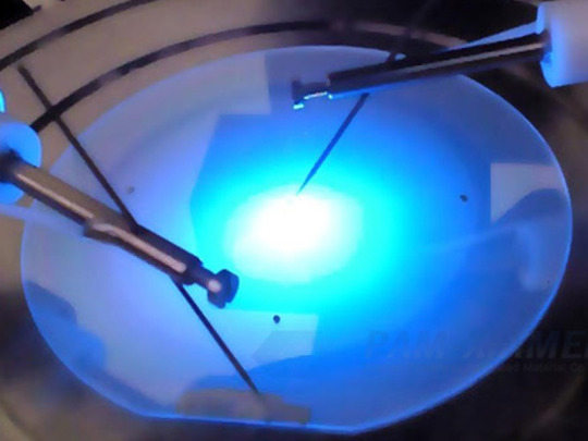
Overview on Epitaxy and its Applications
Epitaxy
Derived from the Greek word epi, which means above, and taxis which indicates an ordered manner. The LED Epi wafer is very reliable. This process forms one or several crystalline thin films that can be of the same or different chemical compositions and it has the structure as the substrate. In the technique of crystallography where natural or artificial crystals are grown on a crystalline substrate, Epitaxy is an important technique that is used.
In nanotechnology and semiconductor fabrication the process is used where it is of commercial importance. Epitaxy is the only affordable method for many semiconductor materials where high-quality crystals are growing. It marks little importance for most thin-film applications, for example, hard or soft coatings, or optical coatings whereas in semiconductor thin-film technology it is critical. In this in electronic and photonic devices such as computer video displays and telecommunication applications, the growth of semiconductor materials forms layers and quantum wells. For maximum technological applications, the desire is for the deposited material to form a crystalline film that concerning the substrate crystal structure has one well-defined orientation. You can purchase wafers from LED Epi wafer supplier.
Applications and Epitaxial Growth of Thin Film Materials
In electronics, optoelectronic and magneto-optics epitaxial growth of thin-film materials has numerous applications. In several ways, growth can occur where the most common is the vapor phase epitaxy (a modification of chemical vapor deposition), where from vapor the atoms for deposition on the substrate are taken and growth occurs at the gaseous/solid interface. On the substrate, solid-phase epitaxy deposits a thin non-crystalline film which is then heated to form a crystalline layer, while in the liquid phase from a liquid source the layers grown in epitaxy are observed.
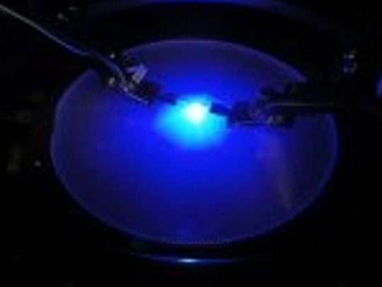
In producing device quality layers the latter is by far the cheapest and easiest route, but in terms of using metal-organic chemical vapor deposition (MOCVD) and molecular beam epitaxy (MBE) is growing. MOCVD and MBE are more versatile but the Initial costs are expensive and with atomic-layer control, it can readily produce multilayer structures, which is basic to Nanoengineering. The LED Epi wafer manufacturer is opted by many.
14 notes
·
View notes
Text
SiC Crystal
We provide four different crystal structure of silicon carbide (SiC) crystal. Namely they are 6H-SiC Wurtzite ( Hexagonal), 4H-SiC Wurtzite ( Hexagonal), 3C-SiC Zinc blende (cubic) and SiC Epi wafer. It is widely used LED, RF, high power devices, high temperature devices and high frequency power devices manufacturing industries to produce quality semiconductor products.
0 notes
Text
Epitaxial (Epi) Wafer Market: Granular View of The Market from Various End-Use Segments
Epitaxy is a method used to grow or lay a single crystalline film or layer over a crystalline-based semiconductor surface or substrate. The deposited substance must have a definite acclimatization with regard to the crystal-based semiconductor substrate. Moreover, Chip developers applies either molten or vapor based foundations to produce such epitaxial over layers. An epitaxial wafer is a wafer of semiconducting substrate made by epitaxial growth for application in microelectronics, photovoltaics and photonics. The market for epitaxial wafers is segmented on the basis of wafer size which includes 50mm to 100mm, 100mm to 150mm, above 150 mm. The market has been also segmented by application which includes LED semiconductor, power semiconductor, and MEMS-based devices among others. Geographically, the market is segmented into North America, Asia Pacific, Europe, Middle East and Africa and South America.
PDF Brochure For Future Advancements @ https://www.transparencymarketresearch.com/sample/sample.php?flag=B&rep_id=24947
Heteroepitaxy and homoepitaxy are two prime methods used for epitaxial deposition. A film or layer is deposited on a substrate of dissimilar composition is known as heteroepitaxy deposition. Laying a film or layer on a surface or substrate of a similar level of conformation is known as homoepitaxy. With the growing demand for high end semiconductor equipment and device and increasing demand for energy efficient LED lights is also fueling the market for epitaxial wafer globally. Increasing focus on reducing the overall consumption of electricity along with growing awareness of green technology among consumers have compelled manufacturers to adopt eco-friendly and energy-efficient lighting for example LED lighting. Furthermore, different governments are also taking up multiple projects and offering subsidies to promote LED lights which are acting as major driving factor for the epi wafer market globally. MEMS devices for instance gyroscopes, pressure sensors, accelerometers, micromirrors, digital compasses and modern pico projectors primarily use epi-wafers with features with thicker epi layers. Lowering manufacturing costs and providing higher device sensitivity and performance is driving the market for epi wafer market globally. The rising demand for high end features of smart devices like tablets and smart phones are having a positive effect on the market for epitaxial wafers. Epitaxial wafers are more effective than bulk wafers owing to its attribute of providing the doping profile of a particular semiconductor device. The deposited layers are generally designed to have different electrical and compositional properties from the underlying wafer. Further, this can be easily adjusted as per the need of the semiconductor equipment or devices. For example, an epitaxial layer on a transistor primarily boosts the transistor’s switching speed and increases its breakdown voltage. Increasing popularity of tablets, smartphone, notebooks, gaming consoles, personal computers and laptops are fueling the demand for epitaxial wafers globally. OEMs (Original Equipment manufacturers) are keen on introducing new 3D NAND integrated devices for example ICs. DRAM (Dynamic random access memory) requires less power and this attribute is another prime factor fueling the market for epitaxial wafers worldwide. Design complexities are one of the major restraining factors for the market which may hinder the growth of the market. However, Introduction of Dynamic random access memory (DRAM) and 3D NAND memory devices are anticipated to boost the demand for epitaxial wafers and it is considered as major opportunity for the market across different economies globally.
Download Table Of Content @ https://www.transparencymarketresearch.com/sample/sample.php?flag=T&rep_id=24947
0 notes
Text
LED Chip and Module Global Market 2018 Development Trend, Segmentation and Industry Forecasts to 2023
Wiseguyreports.Com Adds “LED Chip and Module Market 2018 Global Analysis, Growth, Trends and Opportunities Research Report Forecasting to 2023”.
New York, NY — (Daily PR News) — 01/05/2018 — Epi/chip. Epitaxy refers to the process of evolving a wafer (sapphire or SiC, for instance) by depositing epitaxial layers on the wafer using MOCVD. Creating the epitaxial layers is the most critical and capital-intensive step in LED manufacturing. After additional wafer processing to create the metal connection, the wafer is cut up (“”diced””) into chips. Although it can be used for different applications, the quality requirements (mainly efficacy) of the epi/chip differ by application.Module (sometimes called light engine). Creation of a module (light engine) is the next step in the LED lighting value chain. The module (light engine) mainly consists of one or more LED packages, secondary optics, a heat sink and an electrical driver. The LEDs are mounted on a PCB (printed circuit board), and the modules (light engines) are integrated with optics and thermal/power management components to optimize the module (light engine) to each application.
The objective of report is to define, segment, and project the market on the basis of product type, application, and region, and to describe the content about the factors influencing market dynamics, policy, economic, technology and market entry etc.
Leading vendors in the market are included based on profile, business performance etc. Vendors mentioned as follows:
Epistar
San’an Opto
Cree
OSRAM
Samsung
Toyoda Gosei
Seoul Semiconductor
Philips Lumileds
ETI
LG Innotek
NiChia
HC SemiTek
Lextar
Lattice Power
OPTO-TECH
Tyntek
Genesis Photonics
Formosa Epitaxy
Changelight
Aucksun
TongFang
Request a Sample Report @ https://www.wiseguyreports.com/sample-request/1794059-global-led-chip-and-module-market-research-report-2011-2023
Based on products type, the report describes major products type share of regional market. Products mentioned as follows:
Lateral Chip
Vertical Chip
Flip Chip
Based on Application, the report describes major application share of regional market. Application mentioned as follows:
General Lighting
Automotive Lighting
Backlighting
Based on region, the report describes major regions market by products and application. Regions mentioned as follows:
Asia-Pacific
North America
Europe
South America
Middle East & Africa
At any Query @ https://www.wiseguyreports.com/enquiry/1794059-global-led-chip-and-module-market-research-report-2011-2023
Table of Contents
1 Market Overview
1.1 Objectives of Research
1.1.1 Definition
1.1.2 Specifications
1.2 Market Segment
1.2.1 by Type
1.2.1.1 Lateral Chip
1.2.1.2 Vertical Chip
1.2.1.3 Flip Chip
1.2.2 by Application
1.2.2.1 General Lighting
1.2.2.2 Automotive Lighting
1.2.2.3 Backlighting
1.2.3 by Regions
6 Market Segmentation by Region
6.1 Market Size
6.1.1 Asia-Pacific
6.1.1.1 Asia-Pacific Market, 2011-2016
6.1.1.2 Asia-Pacific Market by Type
6.1.1.3 Asia-Pacific Market by Application
6.1.2 North America
6.1.2.1 North America Market, 2011-2016
6.1.2.2 North America Market by Type
6.1.2.3 North America Market by Application
6.1.3 Europe
6.1.3.1 Europe Market, 2011-2016
6.1.3.2 Europe Market by Type
6.1.3.3 Europe Market by Application
6.1.4 South America
6.1.4.1 South America Market, 2011-2016
6.1.4.2 South America Market by Type
6.1.4.3 South America Market by Application
6.1.5 Middle East & Africa
6.1.5.1 Middle East & Africa Market, 2011-2016
6.1.5.2 Middle East & Africa Market by Type
6.1.5.3 Middle East & Africa Market by Application
6.2 Market Forecast
6.2.1 Asia-Pacific Market Forecast, 2017-2022
6.2.2 North America Market Forecast, 2017-2022
6.2.3 Europe Market Forecast, 2017-2022
6.2.4 South America Market Forecast, 2017-2022
6.2.5 Middle East & Africa Market Forecast, 2017-2022
8 Major Vendors
8.1 Epistar
8.1.2 Profile
8.1.2 Business Performance (Sales Revenue, Cost, Gross Margin)
8.2 San’an Opto
8.2.1 Profile
8.2.2 Business Performance (Sales Revenue, Cost, Gross Margin)
8.3 Cree
8.3.1 Profile
8.3.2 Business Performance (Sales Revenue, Cost, Gross Margin)
8.4 OSRAM
8.4.1 Profile
8.4.2 Business Performance (Sales Revenue, Cost, Gross Margin)
8.5 Samsung
8.5.1 Profile
8.5.2 Business Performance (Sales Revenue, Cost, Gross Margin)
8.6 Toyoda Gosei
8.6.1 Profile
8.6.2 Business Performance (Sales Revenue, Cost, Gross Margin)
8.7 Seoul Semiconductor
8.7.1 Profile
8.7.2 Business Performance (Sales Revenue, Cost, Gross Margin)
8.8 Philips Lumileds
8.8.1 Profile
8.8.2 Business Performance (Sales Revenue, Cost, Gross Margin)
8.9 ETI
8.9.1 Profile
8.9.2 Business Performance (Sales Revenue, Cost, Gross Margin)
8.10 LG Innotek
8.10.1 Profile
8.10.2 Business Performance (Sales Revenue, Cost, Gross Margin)
8.11 NiChia
8.12 HC SemiTek
8.13 Lextar
8.14 Lattice Power
8.15 OPTO-TECH
8.16 Tyntek
8.17 Genesis Photonics
8.18 Formosa Epitaxy
8.19 Changelight
8.20 Aucksun
8.21 TongFang
Buy Now @ https://www.wiseguyreports.com/checkout?currency=one_user-USD&report_id=1794059
Continued….
Contact Us: [email protected]
Ph: +1-646-845-9349 (US) ; Ph: +44 208 133 9349 (UK)
The post LED Chip and Module Global Market 2018 Development Trend, Segmentation and Industry Forecasts to 2023 appeared first on Daily Press Release News To Whole World.
from Daily Press Release News To Whole World https://www.dailyprnews.com/led-chip-and-module-global-market-2018-development-trend-segmentation-and-industry-forecasts-to-2023/
0 notes
Text
Epitaxial Wafer Market Forecast 2018-2026, Latest Trends And Opportunitie.
Market Overview
Epitaxial Wafer, also known as Epi-wafer is placed over other silicon wafer through epitaxial process. Epitaxy is a process in which a monocrystalline silicon layer is deposited over the polished crystal surface of a silicon wafer. This wafer acts as semiconducting substrate for applications such as microelectronics, photovoltaic, and photonics. There are two types of epitaxial wafer named; Homoepitaxy and Heteroepitaxy.
Major factor driving growth of the epitaxial wafer market is increasing use of LED lighting across the globe and this is fueling demand for epitaxial wafer. For instance, according to Coherent Market Insights’ analysis, the rate of LED lighting penetration in 2015 was 15% and it has increased to 27% in 2016, globally. The factor attributed to growth of LED lighting is increasing demand for energy efficient lighting products that help in reducing consumption of electricity and this is a major factor for replacing conventional lighting products with LED lighting across residential, commercial, and industrial sectors. LED lights are mainly incorporated with number of Ics.
This report provides in-depth analysis of epitaxial wafer market size (US$ Mn), and Compound Annual Growth Rate (CAGR %) for the forecast period (2018 – 2026), considering 2017 as the base year
Request Sample Copy of this Report @https://www.coherentmarketinsights.com/insight/request-sample/2277
Market Dynamics
Increasing installation of solar panel across the globe is one of the factors driving growth of the market. This is owing to growing awareness among consumers about the advantages of using solar energy. For instance, according to Coherent Market Insights’ analysis, number of solar panel installed in 2015 was 50.7 gigawatt and it has reached up to 76.7 gigawatt in 2016, globally. These solar panels are equipped with cells that are created from silicon wafers as silicon wafer have semiconducting properties. The usage of silicon wafer in solar cells has led to increasing efficiency of solar panel, which means it generates more power per unit compared to conventional material that used in solar cells. Thus, advantages offered by silicon wafer will positively increase the usage of silicon wafer for manufacturing of solar cells. Thus, increasing demand for silicon wafer will drive wafer manufacturers to coat that silicon wafer with epitaxial layer in order to increase the efficiency of the panel. The coating of epitaxial wafer further contributes in increasing performance of solar panels. Hence, all these factors are expected to propel demand for epitaxial wafer over the forecasted period.
Detailed Segmentation:
Global Epitaxial Wafer Market, By Deposition Type:
Heteroepitaxy
Homeoepitaxy
Global Epitaxial Wafer Market, By Wafer Size:
50mm to 100mm
100mm to 150mm
Above 150mm
Global Epitaxial Wafer Market, By Application:
LED Semiconductor
Power Semiconductor
MEMS-based devices
Request For Customization @ https://www.coherentmarketinsights.com/insight/request-customization/2277
Major players operating in the global epitaxial wafer market include EpiWorks Inc., Global Wafers Japan Co. Ltd., Nichia Corporation, SHOWA DENKO K.K., Siltronic AG, Desert Silicon Inc., Electronics and Materials Corporation Ltd. Intelligent Epitaxy Technology Inc.IQE plc. , Jenoptic AG, MOSPEC Semiconductor Corporation, Norstel AB, Ommic S.A., Silicon Valley Microelectronics Inc. ,SVT Associates Inc. Universal Wafer Inc., Wafer Works Corporation, Xiamen Powerway Advanced Materials Co. Ltd., and Visual Photonics Epitaxy Co. Ltd.
About Coherent Market Insights:
Coherent Market Insights is a prominent market research and consulting firm offering action-ready syndicated research reports, custom market analysis, consulting services, and competitive analysis through various recommendations related to emerging market trends, technologies, and potential absolute dollar opportunity.
Contact Us:
Mr. Shah
Coherent Market Insights
1001 4th Ave,
#3200
Seattle, WA 98154
Tel: +1-206-701-6702
Email: [email protected]
0 notes
Text
LG Innotek Unveils the World's First 70mW UV-C LED
SEOUL, South Korea, Feb. 23, 2017 /PRNewswire/ -- LG Innotek today announced that the company has developed the world's first 70mw UV-C LED for sterilization applications. As its sterilization performance is 1.5 times higher than the competitor's 45mW module.
UV-C LED produces the short wavelength ultraviolet rays in the range of 200 -- 280nm, allowing it to be used for sterilization purpose. It prevents the proliferation of bacteria by destroying their DNA. LG Innotek's product emits UV in the range of 280nm.
Until now, UV-C LED has been mainly applied in small sanitary products because its low optical power led to low sterilization performance. The power of LEDs for toothbrush sterilizers is 1mW and that for sterilizing the water tank of humidifier is 2mW.
LG Innotek improved UV-C LED's optical power to 70mW by utilizing its proprietary LED vertical chip technology. While the product measures only 6mm in both its length and width, its sterilization performance is the world's best.
The company overcomes the UV output limit with specialized LED chip technology. The epitaxial structure design and vertical chip technology to maximize light extraction have increased the output and ensured quality reliability by effectively exhausting heat.
As the company's product is compact and boasts high sterilization performance, it can be applied to various fields such as water purifiers and air purifiers as it allows you to sterilize flowing water and air.
It is also good for use in hardening equipment in the manufacturing industry. The UV output is strong, the performance of the curing device can be enhanced.
Manufacturers of water purification, cleaning and curing device can benefit from stable supply of UV-C LEDs optimized for respective purposes from LG Innotek. Because LG Innotek is equipped with a consistent production system that produces Epi-wafers, chips, packages, and modules, and offers its products to its customers after rigorous quality management.
Along with its 280nm UV-C LED, LG Innotek has a lineup of LEDs from 365nm, 385nm, 395nm, and 405nm UV-A LEDs for general industrial purposes to 305nm UV-B LEDs for bio and medical purposes.
Ho-rim Jung, the vice president of LED marketing division said, "We are expecting expansion of UV-C LED application field by developing 70mW product. We will continue to show high-quality innovative products."
According to Yole Development, a market research firm, the UV LED market is forecast to grow from 130 million USD in 2015 to 270 million USD in 2017.
[Photo: http://ift.tt/2lz2eqr]
About LG Innotek Co,.Ltd.
LG Innotek is a cutting-edge materials and components manufacturer and an affiliate of LG group. The company's business units include core components for LED, mobile, automotive, display, semiconductor and IoT. Further, the company has cooperated closely with mobile device, home appliance and automotive companies, producing camera modules, automotive electronic components, wireless communication module, substrate materials.
In the LED sector, LG Innotek has vertically integrated the entire manufacturing process from Epi-wafers and chips to packages and modules, while providing LED products optimized for lighting, mobile, display and automotive applications.
LG Innotek is headquartered in Seoul, Korea and its sales subsidiary is located in San Jose and Chicago, United States. For more information, please refer to the website: www.lginnotek.com or led.lginnotek.com
Media Contact
Beop-min Oh
Communication Team
LG Innotek
Seoul, Republic of Korea
Phone: +82-2-3777-0158
E-mail: [email protected]
To view the original version on PR Newswire, visit:http://ift.tt/2lyRDM4
Read this news on PR Newswire Asia website: LG Innotek Unveils the World's First 70mW UV-C LED
0 notes
Text
Silicon EPI Wafers Market Global Production, Growth, Share, Demand and Applications Forecast to 2030
Silicon EPI Wafers Market: Introduction
Silicon EPI wafers were first developed in 1966 and gained commercial acceptance in the 1980s.
Silicon EPI wafer is an exotic semiconducting material. It is combined with an epitaxial layer that is a deposition of a crystalline layer over a crystalline-based semiconductor substrate, called silicon EPI wafer. These wafers are used as a high purity layer and for the formation of thick dopes.
Silicon EPI wafers (also called epitaxial wafers) is a wafer of semiconductor material made up of epitaxy, for use in photonics, microelectronics, spintronics, and photovoltaics.
Rise in Demand from Integrated Circuits, Sensors, in Consumer Electronics, and Automotive and Telecommunication Industry
Globally, development of efficient and advanced technology, and rising demand for electronic devices including laptops, tablets, gaming consoles, and smartphones, are leading to a thriving electronics and semiconductor industry. Advantageous properties of semiconductors are the prime growth drivers of the silicon EPI wafers market.
Use of LED lighting across residential, commercial, and industrial sectors globally is also driving the growth of the silicon EPI wafers market.
Silicon EPI wafers are used in the manufacturing of various semiconductor components. They are the building blocks for different semiconductors which are used in the smallest sensors in light bulbs to the most advanced space shuttle.
The market holds high potential in electronics and IT & telecommunication industries. Thus, increase in adoption of advance wafer technology in portable electronics is expected to trigger the demand for silicon EPI wafers in the future.
Demand for semiconductors of silicon EPI wafers has increased in recent years due to their high efficiency, light weight, and less space consumption. They are widely use in microprocessors and wearable technologies.
Planning to lay down future strategy? Perfect your plan with our report sample here https://www.transparencymarketresearch.com/sample/sample.php?flag=S&rep_id=82097
Asia Pacific to Lead the Silicon EPI Wafers Market
In terms of region, the global silicon EPI wafers market can be divided into North America, Europe, Asia Pacific, Middle East & Africa, and Latin America.
Asia Pacific has the largest market share owing to high demand for LEDs, as they offer better brightness, efficiency, and intensity.
Asia Pacific is anticipated to witness fastest growth in the global silicon EPI wafers market throughout the forecast period, as a large number of manufacturers operate in the region, especially in China.
Furthermore, the global silicon EPI wafers market in Europe and Middle East & Africa is expected to expand at a significant rate during the forecast period. On the other hand, the market in South America is predicted to grow at a steady pace during the forecast period.
Key Players Operating in the Global Silicon EPI Wafers Market
Epiworks Inc.
Global Wafers Japan Co. Pvt Ltd
Nichia Corporation
Siltronics AG
Silicon Valley Microelectronics Inc.
Xiamen Powerway Advanced Material Co. Ltd
Visual Photonics Epitaxy Co. Ltd
Wafer Work
American Elements
Global Silicon EPI Wafers Market: Research Scope
Global Silicon EPI Wafers Market, by Wafer Size
6-Inch
8-Inch
12-Inch
Others
Global Silicon EPI Wafers Market, by Type
Homoepitaxy
Hetroepitaxy
Global Silicon EPI Wafers Market, by Application
LED
Power Semiconductors
MEMS-based Devices
Laptops and Tablets
Others
Global Silicon EPI Wafers Market, by Region
Asia Pacific
North America
Europe
LAMEA
China
Japan
India
South Korea
Rest of Asia Pacific
United States
Canada
Mexico
Rest of North America
United Kingdom
Germany
France
Italy
Rest of Europe
Latin America
Middle East
Africa
Looking for exclusive market insights from business experts? Buy now Report here https://www.transparencymarketresearch.com/checkout.php?rep_id=82097<ype=S
This study by TMR is all-encompassing framework of the dynamics of the market. It mainly comprises critical assessment of consumers’ or customers’ journeys, current and emerging avenues, and strategic framework to enable CXOs take effective decisions.
Our key underpinning is the 4-Quadrant Framework EIRS that offers detailed visualization of four elements:
Customer Experience Maps
Insights and Tools based on data-driven research
Actionable Results to meet all the business priorities
Strategic Frameworks to boost the growth journey
The study strives to evaluate the current and future growth prospects, untapped avenues, factors shaping their revenue potential, and demand and consumption patterns in the global market by breaking it into region-wise assessment.
The following regional segments are covered comprehensively:
North America
Asia Pacific
Europe
Latin America
The Middle East and Africa
The EIRS quadrant framework in the report sums up our wide spectrum of data-driven research and advisory for CXOs to help them make better decisions for their businesses and stay as leaders.
0 notes
Last Seen Blogs

speedbaegon
part 8 animated when

character-by-carly
Bnw Photography


3heads-or-tails4-blog
"Pack of Cigarettes"

fanundertalegirlpl-blog
SpeedPainty / FanArty