#multiple wafer processing
Explore tagged Tumblr posts
Visit Tumblr Blog
Explore Tumblr blogs with no restrictions, modern design and the best experience.
Last Seen Tumblr Blogs


Fun Fact
Tumblr Inc. is funded by 13 investors.
Text
“As I imagine those lines thickening, I become immersed in a photograph of the philosopher Gilles Deleuze, taken during a visit to Big Sur in the mid-1970s, as he sits on the California beach examining its sands and the breathing striations of the silica terrain. The world remaking itself in waves, bit by bit and pebble by pebble. In trying to place the image, I also think about how just up the 101 freeway from where Deleuze was sitting, silicon was being repurposed as the physical medium of synthetic computational intelligence, in the areas near Palo Alto in a “valley” already having been named in honor of this element. For me these are conjoined, and not just by their geographic proximity: Deleuze on the beach contemplating (we might assume) what he called “the plane of immanence,” the field from which all potential forms emerge, and Intel’s initial approximations of microprocessor technology for universal computation, putting a mini-Turing machine on a silicon wafer. In different ways and for different ends, both grapple with matter as vibrant, contingent, and mutable, as reproduced in the careful calculation of sets of differences drawn from particular virtual possibilities. At the end of the day, Deleuze’s philosophy is more about chemistry than computation, continuities more than discrete digitalizations, but his philosophical imagery of worlds appearing from the multiplication of imminent processes and generic diagrams, on oscillations of the physical and the virtual, is not unfamiliar to the projects of information realism. In the words of the late Friedrich Kittler, “Silicon is nature! Silicon is nature calculating itself. If you leave out the part of engineers who write little structures on silicon you see one part of matter calculating the rest of matter.” — Benjamin Bratton, The Stack
20 notes
·
View notes
Text
havent posted a poll with my own silly in a while. time to go brrrr
#rain world#iterator#rain world iterator#rain world oc#rw iterator#rw oc#iterator oc#rw iterator oc#rain world iterator oc#hyperspecific poll#hyperspecific polls#hyperspecific wafer polls#polls that contain my ocs
7 notes
·
View notes
Text
The Immediate Tutorial Process of “Cookie Run: Witch’s Castle”
⚙️ This tutorial is fresh off the printer unlike the others I’ve done before this one, so let’s get down to it under the context that you passed the DevPlay login page and downloaded everything. Spoilers are imminent, duh!
Enter Your Name
⚙️ This’ll be your username for the game, so make it a good one… or use the generator to get an idea for one.

Level 1
⚙️ According to relevant sources, the Witch’s Castle used to house a whole coven of Witches and then some. In the opening sequences, this is where *this* iteration of GingerBrave is baked to wake up- once again- in a fiery hot oven on a scorching hot metal pan. This is where the tutorial begins.
Moves: 999 (it’s practically impossible to fail)
Chosen Cookie: 🍪 GingerBrave
Controls - Making Moves: Tap a jelly that’s part of a group of two or more jellies of matching colors to pop them and interact with various board gimmicks.
🎯 Objectives - Vials: Pop jellies next to these explosive potions to send them into an overarching enemy target. In this case, it’s the Oven Doors. 10-15 vials should clear the level, where GingerBrave gracelessly falls out the window after a scripted tap prompt.

Level 2
⚙️ Uh oh! GingerBrave’s graceless jump away from the Shadow Witch just landed him in a horde of zombie-like Spoiled Cookies! But this time, someone else is here to bail him out.
Moves: 50
Chosen Cookie: 💫🪄 First Cream Cookie (Currently hidden)
🎯 Objective - Spoiled Cookies: Practically undead Cookie heads. Pop Jellies next to them to clear them. In this level and most likely in future levels, they will appear in waves. For this level, there are 50 spoiled cookies spread across three waves. Clear them all to win!
Power Jellies: These jellies will appear in the tapped square after clearing large groups of jellies in one move. Tap them to activate them as is, or tap one when it’s next to another power jelly for a stronger effect. These jellies mimic similar power-ups in similar blockbusting puzzle games, where they’ll pop jellies, destroy obstacles, and interact with objectives.
Cookie Skills: Each Cookie has one. Tap the Cookie when the Energy gauge is full to enable it, then tap your target square on the board to activate it. In this tutorial, this feature is unlocked on the 3rd and final wave of spoiled Cookies, where this skill will clear them all.


Episode 1, Chapter 1
⚙️ After GingerBrave escapes, he finds himself in the Witch’s Castle where he finds a witch-lookalike Cookie who taunts him in his efforts to escape out the window in… an attitude that almost matches mine?! NO WAY! Better clear the way for this guy, since he just had a bad collision! Start with these two obstacles, which require two Golden Star Jellies to clear.
Resources - Golden Star Jellies: You’ll get another Star after clearing level 2. That’s right. *Another.* You got one for level 1 too. Use them to progress the story and unlock new features. In this case, you’re clearing obstacles… but not for long. Better get back to the board for more Stars! Some levels will award multiple stars… like level 3.

Level 3
⚙️ Back to work, you know the drill. We need FOUR Golden Star Jellies to clear the immediate area this time.
Moves: 40
Skills: Disabled
Chosen Cookie: 🍪 GingerBrave
🎯 Objective - Wafers: These squares crumble once you pop jellies next to them. They are not affected by gravity if anything below them are cleared out from under them. In this level, there are 36 wafers in a 6x6 square. Clear all of them to win!
Bonus - Coin Bonuses & Level Completion: After clearing the level, power jellies are added to the board based on how many moves you have left. Afterwards, they all get detonated at once to pop jellies on the board to score some bonus coins on top of your base prize, tentatively being 160 Coins extra at most. More moves, more Coins! Each remaining move scores 10 Coins.
Rewards: 1+3 Golden Star Jellies, 50+160 Coins


Level 4
⚙️ Missing stairs? Get another Star. This level loosens the scripted restraints and lets you play the level as you want. Just clear the Wafers and move on already!
Moves: 38
🎯 Wafers: 49
Skills: Disabled
Chosen Cookie: 🍪 GingerBrave
Rewards: 1 Golden Star Jelly, 50+160 Coins

⚙️ That should be the last of it. From here, you’ll unlock the second floor and get a free progression reward of 20 Crystals. The rest of the user interface will also open up to you and the tutorial wheels essentially detach from here. There are some other tutorials and stuff that’ll open up as you click on them, but you can explore those whenever your brain catches up with everything. Happy Puzzling!


(Return to the Master Post) 🔗
#crepe archives#cookie run witch’s castle#gingerbrave#shadow witch#first cream cookie#witchberry cookie#cookie run
7 notes
·
View notes
Text
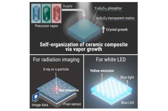
3D pattern generation via chemical vapor deposition of ceramic eutectic system for novel solid-state phosphors
The eutectic structure of metals and ceramics occurs when multiple solid phases solidify from a liquid phase, forming a three-dimensional (3D) pattern through a self-organizing phenomenon. Traditionally, it was believed that eutectic structures could only be obtained through a melt-solidification process. Researchers at Yokohama National University (YNU) have developed a chemical vapor deposition (CVD) process that allows precursor gases to react and generate solid-state composites with ordered structures in a YAG (yttrium alumina garnet)-alumina ceramic eutectic system. In their study, they observed the growth of spatially ordered rod- and lamellar-shaped YAG crystals within an alumina matrix on a sapphire wafer under Al-rich conditions. Conversely, under Y-rich conditions, they observed the growth of ordered alumina crystals with a YAG matrix. The choice of sapphire seed crystal and the composition of the precursor determined the 3D patterns. Compared with the melt-solidification process, the CVD process expanded the range of chemical compositions that could generate such patterns.
Read more.
#Materials Science#Science#Chemical vapor deposition#Ceramics#Phosphors#Eutectic#Phases#Yttrium alumina garnet#Yttrium#Alumina#Yokohama National University
14 notes
·
View notes
Text

The factories that make chips are expensive AF — many billions of dollars — but the process isn’t expensive to run at scale. It’s a little bit like silkscreening t-shirts, in multiple color layers, only shrunk way down and the “ink” is applied by light through tiny masks. Each printed wafer is then cut apart into hundreds of chips.
When people came up with this process in the 1960s, it was low-resolution and the details (transistors) were visible to the naked eye. Since then it’s been a process of iteration where people keep refining the techniques and, about every 18 months, retool or rebuild the factories to make chips with everything half the size as before. That’s where Moore's Law comes from.
“SCIENCE: IT WORKS, BITCHES” —xkcd
Have you ever wondered how tech technicians recover data from faulty flash and memory whose data cannot be recovered by normal methods.
55K notes
·
View notes
Text
Panel Level Packaging Market
Panel Level Packaging Market Size is forecast to reach $3.5 billion by 2026, at a CAGR of 18.5% during 2021–2026.
🔗 𝐆𝐞𝐭 𝐑𝐎𝐈-𝐟𝐨𝐜𝐮𝐬𝐞𝐝 𝐢𝐧𝐬𝐢𝐠𝐡𝐭𝐬 𝐟𝐨�� 𝟐𝟎𝟐𝟓-𝟐𝟎𝟑𝟏 → 𝐃𝐨𝐰𝐧𝐥𝐨𝐚𝐝 𝐍𝐨𝐰
Panel Level Packaging (PLP) Market is gaining traction as a cutting-edge advancement in semiconductor packaging, offering greater scalability, cost efficiency, and throughput compared to traditional wafer-level packaging. By processing multiple semiconductor dies on larger panel-sized substrates, PLP enables high-volume production and supports the growing demand for compact, high-performance electronics used in AI, 5G, IoT, and automotive applications. This technology reduces material waste, lowers production costs, and enhances design flexibility. As device miniaturization and chip complexity increase, PLP is becoming a vital solution for next-generation electronics, driving innovation across consumer, industrial, and communications sectors worldwide.
📏 𝟏. 𝐃𝐞𝐦𝐚𝐧𝐝 𝐟𝐨𝐫 𝐌𝐢𝐧𝐢𝐚𝐭𝐮𝐫𝐢𝐳𝐚𝐭𝐢𝐨𝐧
As electronic devices shrink in size while increasing in functionality, PLP offers high-density packaging solutions that support compact and lightweight designs.
⚙️ 𝟐. 𝐂𝐨𝐬𝐭 𝐄𝐟𝐟𝐢𝐜𝐢𝐞𝐧𝐜𝐲 𝐚𝐭 𝐒𝐜𝐚𝐥𝐞
PLP enables processing on larger panel substrates (compared to wafers), reducing per-unit packaging costs and improving manufacturing throughput.
📶 𝟑. 𝐆𝐫𝐨𝐰𝐭𝐡 𝐢𝐧 𝟓𝐆, 𝐀𝐈, 𝐚𝐧𝐝 𝐈𝐨𝐓 𝐃𝐞𝐯𝐢𝐜𝐞𝐬
Emerging technologies require high-performance, high-bandwidth, and low-latency semiconductor solutions — PLP supports these needs through advanced interconnects and efficient thermal management.
🚗 𝟒. 𝐀𝐮𝐭𝐨𝐦𝐨𝐭𝐢𝐯𝐞 𝐄𝐥𝐞𝐜𝐭𝐫𝐨𝐧𝐢𝐜𝐬 𝐁𝐨𝐨𝐦
The rise of autonomous and electric vehicles is driving demand for robust, reliable, and compact semiconductor packages, which PLP is well-suited to deliver.
🔬 𝟓. 𝐀𝐝𝐯𝐚𝐧𝐜𝐞𝐬 𝐢𝐧 𝐒𝐞𝐦𝐢𝐜𝐨𝐧𝐝𝐮𝐜𝐭𝐨𝐫 𝐃𝐞𝐬𝐢𝐠𝐧
With increasing chip complexity, PLP supports heterogeneous integration (multiple dies or components in one package), enabling better performance and functionality.
𝐓𝐨𝐩 𝐊𝐞𝐲 𝐏𝐥𝐚𝐲𝐞𝐫𝐬:
Applied Materials | Western Digital | HARMAN International | Analog Devices | supor | Motorola Solutions | NXP Semiconductors | Sony Danfoss | TSMC | Xiaomi Technology | Midea America | Haier
#SemiconductorIndustry #TechManufacturing #NextGenElectronics #ElectronicsDesign #TechInnovation #SmartManufacturing #FutureOfTech #HighDensityPackaging #ScalableTech #CostEfficientPackaging #PanelProcessing

0 notes
Text
Wafer Carrier Tray Market: Integration with Smart Building Solutions by 2025-2032

MARKET INSIGHTS
The global Wafer Carrier Tray Market size was valued at US$ 567.4 million in 2024 and is projected to reach US$ 934.1 million by 2032, at a CAGR of 7.43% during the forecast period 2025-2032. This growth aligns with the expanding semiconductor industry, which itself is projected to grow from USD 579 billion in 2022 to USD 790 billion by 2029 at a 6% CAGR.
Wafer carrier trays are specialized containers designed to safely transport and store semiconductor wafers during manufacturing processes. These precision-engineered trays protect delicate silicon wafers from contamination and physical damage while ensuring proper handling through various fabrication stages. Common variants include 150mm, 200mm, and 300mm wafer trays, with the 300mm segment currently dominating due to industry adoption of larger wafer sizes for improved manufacturing efficiency.
The market growth is driven by several key factors, including increased semiconductor production capacity globally and stricter cleanliness requirements in fabrication facilities. While the semiconductor segment accounts for approximately 85% of wafer tray usage, the solar energy sector is emerging as a secondary growth driver. Recent developments include advanced polymer formulations that reduce particle generation and static charge accumulation, with key players like Entegris and Shin-Etsu Polymer leading innovation in materials science for wafer handling solutions.
MARKET DYNAMICS
MARKET DRIVERS
Expansion of Semiconductor Manufacturing to Fuel Demand for Wafer Carrier Trays
The global semiconductor industry, valued at $579 billion in 2022, is projected to reach $790 billion by 2029, growing at a 6% CAGR. This rapid expansion directly correlates with increased demand for wafer carrier trays as they are essential for handling delicate silicon wafers during manufacturing and transportation. With foundries expanding production capacity to meet the insatiable demand for chips across automotive, IoT, and consumer electronics sectors, semiconductor manufacturers are requiring more sophisticated wafer handling solutions. Modern wafer carrier trays are engineered to minimize particle contamination – a critical factor as feature sizes shrink below 5nm nodes where even microscopic contaminants can ruin chips worth thousands of dollars.
Transition to Larger Wafer Sizes Accelerating Market Growth
The industry’s ongoing migration from 200mm to 300mm wafer processing continues to drive replacement demand for carrier trays. While 300mm wafers now represent over 75% of global silicon area processed, many analog and power semiconductor manufacturers still operate 200mm fabs, creating a sustained dual-market demand. The transition allows for 2.25x more chips per wafer but requires complete requalification of handling equipment including carrier trays to ensure compatibility. This technological migration presents substantial revenue opportunities for tray manufacturers able to meet the exacting specifications for 300mm processing environments where thermal stability and cleanroom compatibility are paramount.
Additionally, the emerging adoption of 450mm wafer prototypes in R&D facilities suggests a future wave of upgrades, though full commercialization remains several years away due to the billion-dollar costs of fab conversions. Industry experts project that the global wafer carrier tray market will maintain steady growth through at least 2030 as multiple generation technologies remain in concurrent production.
MARKET RESTRAINTS
High Material Costs and Supply Chain Constraints Impacting Market Expansion
The wafer carrier tray market faces significant headwinds from volatile raw material pricing, particularly for specialized engineering plastics and advanced composites. High-purity polycarbonate and PEEK polymer prices have fluctuated between 15-25% annually since 2020, squeezing manufacturer margins. The sophisticated molding and machining equipment required for tray production represents a multi-million dollar investment, creating high barriers to entry. These capital-intensive requirements favor established players but limit market expansion and technological diversification.
Additional constraints include:
Supply Chain Fragility The global semiconductor equipment supply chain remains vulnerable to geopolitical tensions and logistics disruptions. With tray manufacturers dependent on specialty chemical suppliers concentrated in specific regions, any trade restrictions or transportation bottlenecks can cause production delays. This was evidenced during recent disruptions where lead times for critical tray components extended from 8 weeks to over 6 months.
Technical Certification Requirements Each new generation of wafer trays must undergo rigorous qualification testing with semiconductor OEMs – a process often requiring 12-18 months. This lengthy certification cycle slows the introduction of innovative materials and designs that could potentially reduce costs or improve performance.
MARKET OPPORTUNITIES
Emerging Photovoltaic Applications Opening New Growth Frontiers
While semiconductor applications dominate current demand, the solar energy sector presents substantial untapped potential for wafer carrier tray manufacturers. The photovoltaic industry processed over 300 million silicon wafers in 2023, with solar cell production capacity expanding at 25% annually in key markets. Unlike semiconductor-grade trays requiring nanometer-level cleanliness, solar wafer handling solutions can utilize more cost-effective materials while still meeting industry specifications. This allows manufacturers to extend their product portfolios with differentiated offerings for the renewable energy sector.
➤ Leading manufacturers are already adapting semiconductor-grade tray technologies to create solar-specific solutions that reduce wafer breakage during transport – a persistent challenge costing PV manufacturers approximately $150 million annually in yield losses.
Furthermore, the development of reusable tray systems for solar wafer handling presents a compelling value proposition, as the industry seeks to improve sustainability metrics. These systems can reduce single-use packaging waste by up to 80% while maintaining the necessary protection for delicate solar wafers during factory transfers.
MARKET CHALLENGES
Increasing Technical Demands Outpacing Material Science Advancements
As semiconductor fabrication pushes toward 2nm and smaller process nodes, wafer carrier trays must meet increasingly stringent requirements that challenge existing material capabilities. Modern trays must simultaneously provide exceptional dimensional stability across temperature fluctuations, extreme chemical resistance to cleaning solvents, and minimize particulate generation – properties that often have competing material requirements. This technical tightrope has led to situations where leading-edge chipmakers reject entire batches of trays due to sub-nanometer measurement deviations detected during qualification.
Other critical challenges include:
Industry Consolidation Pressures The wafer carrier tray market has seen accelerating consolidation, with the top five manufacturers now controlling over 60% of global capacity. This creates significant competitive barriers for mid-sized players attempting to invest in next-generation tray technologies, potentially slowing overall innovation in the sector.
AI-Driven Quality Expectations The adoption of AI-based wafer inspection systems in fabs has dramatically increased detection sensitivity for tray-related defects. Where human inspectors might have overlooked minor imperfections, machine vision systems flag them as critical failures – requiring tray manufacturers to implement near-zero-defect manufacturing processes that significantly increase production costs.
WAFER CARRIER TRAY MARKET TRENDS
Semiconductor Industry Expansion Driving Demand for Wafer Carrier Trays
The global wafer carrier tray market is experiencing significant growth due to the rapid expansion of the semiconductor industry. With the semiconductor market projected to grow from $579 billion in 2022 to $790 billion by 2029 at a 6% CAGR, demand for reliable wafer handling solutions has intensified. Wafer carrier trays play a critical role in protecting delicate semiconductor wafers during manufacturing, transportation, and storage. The increasing adoption of 300mm wafers, which now account for over 75% of all semiconductor wafers produced, has particularly boosted demand for larger capacity trays. Furthermore, the industry’s shift toward more complex 3D NAND and advanced logic nodes requires superior contamination control, positioning high-performance wafer carriers as essential components in fab operations.
Other Trends
Material Innovation for Advanced Nodes
Manufacturers are increasingly focusing on developing contamination-resistant materials for wafer carrier trays to meet the stringent requirements of sub-7nm semiconductor fabrication. Traditional polycarbonate trays are being supplemented with advanced polymer blends featuring static-dissipative properties and ultra-low particulate generation. The market for specialized material solutions is growing at approximately 9% annually, outpacing standard tray segments. This trend aligns with semiconductor makers’ need to minimize yield loss in advanced processes where even nanometer-scale contaminants can cause significant device failures. Recent developments in carbon fiber-reinforced composites are particularly promising for handling larger wafers while maintaining dimensional stability.
Renewable Energy Sector Adoption
The solar energy sector is emerging as a substantial consumer of wafer carrier trays, driven by massive investments in photovoltaic manufacturing capacity. While the semiconductor segment still dominates with 82% market share in wafer tray applications, solar wafer handling now accounts for nearly 15% of total demand and is growing at 11% CAGR. This growth correlates with solar panel manufacturers’ transition to larger 210mm wafers, requiring redesigned carrier solutions. Unlike semiconductor-grade trays that emphasize contamination control, solar applications prioritize durability and cost-efficiency, creating distinct product segments within the market. The increasing automation in solar panel production lines has further accelerated adoption of standardized carrier systems to enable seamless robotic handling.
COMPETITIVE LANDSCAPE
Key Industry Players
Manufacturers Focus on Product Innovation to Cater to Evolving Semiconductor Demand
The global wafer carrier tray market features a mix of established players and emerging competitors, primarily concentrated across Asia-Pacific and North America. Entegris currently leads the market, holding approximately 18-22% revenue share in 2024 due to its comprehensive portfolio of contamination-control solutions and strategic acquisitions like the purchase of CMC Materials in 2022. The company’s dominance stems from its ability to provide complete wafer handling ecosystems.
Shin-Etsu Polymer and Miraial Co., Ltd. collectively account for nearly 25-30% of the Asian market, benefiting from their proximity to semiconductor fabrication hubs in Japan, Taiwan, and South Korea. These companies are investing heavily in R&D to develop advanced polymer compounds that reduce particulate generation – a critical requirement for next-generation chip manufacturing.
The competitive intensity is increasing as mid-sized players like 3S Korea and Gudeng Precision expand their production capacities. 3S Korea recently announced a $30 million facility expansion to meet growing demand from Samsung Electronics and SK Hynix. These companies are gradually eroding the market share of larger players through competitive pricing and faster delivery times.
Meanwhile, European suppliers such as SPS-Europe are differentiating themselves through specialized designs for compound semiconductor applications, particularly in the power electronics segment. The industry is witnessing a surge in strategic partnerships, with Ferrotec recently collaborating with several Chinese foundries to localize production.
List of Key Wafer Carrier Tray Manufacturers Profiled
Entegris (U.S.)
Shin-Etsu Polymer (Japan)
Miraial Co., Ltd. (Japan)
3S Korea (South Korea)
Chuang King Enterprise (Taiwan)
EPAK Electronics (Germany)
Dainichi Shoji K.K. (Japan)
Gudeng Precision (Taiwan)
E-SUN (China)
SPS-Europe (Germany)
Peak International (U.S.)
Ferrotec (Japan)
Segment Analysis:
By Type
300 mm Wafer Tray Segment Leads Due to High Adoption in Advanced Semiconductor Manufacturing
The market is segmented based on type into:
150 mm Wafer Tray
200 mm Wafer Tray
300 mm Wafer Tray
Other specialized trays
By Application
Semiconductor Segment Dominates with Increasing Demand for Advanced Chips and IoT Devices
The market is segmented based on application into:
Semiconductor manufacturing
Solar energy panel production
Research and development
By Material
Plastic Composite Segment Gaining Traction Due to Lightweight and Cost Advantages
The market is segmented based on material into:
High-purity plastics
PP (Polypropylene)
PEEK (Polyether ether ketone)
Others
Advanced composites
Stainless steel
By End-Use Industry
Foundries Segment Leads with Expanding Semiconductor Production Capacity Worldwide
The market is segmented based on end-use industry into:
Semiconductor foundries
IDMs (Integrated Device Manufacturers)
Solar panel manufacturers
Research institutions
Regional Analysis: Wafer Carrier Tray Market
North America The North American wafer carrier tray market is driven by strong semiconductor manufacturing capabilities and significant R&D investments in advanced fabrication technologies. The U.S. holds the dominant position, accounting for approximately 38% of regional revenue, supported by major semiconductor hubs like Arizona and Texas. Stringent contamination control standards and adoption of Industry 4.0 practices in wafer handling are accelerating demand for high-precision 300mm trays. However, rising material costs and supply chain disruptions present challenges. The market benefits from government initiatives like the CHIPS Act, which allocates $52 billion to bolster domestic semiconductor production, creating indirect demand for wafer handling solutions.
Europe Europe’s wafer carrier tray market exhibits steady growth, characterized by specialization in automotive and industrial semiconductor applications. Germany leads regional consumption due to its robust MEMS (Micro-Electro-Mechanical Systems) manufacturing sector. The region shows strong preference for 200mm trays owing to mature fabrication facilities, though 300mm adoption is growing among foundries upgrading capacity. Environmental regulations regarding polymer materials influence product development, with manufacturers focusing on recyclable and cleanroom-compatible solutions. The European Chips Act aims to double the region’s semiconductor market share to 20% by 2030, indicating long-term potential for wafer handling equipment suppliers.
Asia-Pacific Asia-Pacific dominates the global wafer carrier tray market, contributing over 60% of worldwide demand. This reflects the region’s concentration of semiconductor fabrication plants, particularly in Taiwan, South Korea, and China. Rapid expansion of 300mm wafer fabs and government-backed semiconductor self-sufficiency initiatives in China are primary growth drivers. Japanese manufacturers lead in high-purity tray production, while Southeast Asia emerges as a cost-effective manufacturing hub. The region faces intense price competition, prompting suppliers to balance cost optimization with contamination prevention – a critical factor given tightening chip yield requirements. India’s nascent semiconductor ecosystem presents future growth opportunities as the country develops its first major fabs.
South America South America represents a niche market primarily serving the solar energy sector’s silicon wafer requirements. Brazil accounts for most regional demand, though volumes remain modest compared to other regions. The lack of advanced semiconductor manufacturing limits adoption of sophisticated carrier trays, with most demand concentrated on basic 150mm and 200mm solutions. Economic instability and limited local production capabilities result in heavy reliance on imports, affecting supply consistency. Nonetheless, growing renewable energy investments and potential nearshoring benefits as global supply chains diversify suggest gradual market development prospects.
Middle East & Africa The MEA wafer carrier tray market remains in early development stages, with activity concentrated in Israel’s specialized semiconductor sector and Gulf Cooperation Council (GCC) countries’ solar energy projects. Limited local fabrication capacity keeps demand minimal, though the region serves as a strategic logistics hub for tray shipments between Asia and Europe. Abu Dhabi’s G42 and Israel’s Tower Semiconductor represent key local demand sources. While not yet a significant market, MEA’s growing technology investment strategies and potential as an alternative manufacturing location warrant long-term monitoring by industry participants.
Report Scope
This market research report provides a comprehensive analysis of the global and regional Wafer Carrier Tray markets, covering the forecast period 2025–2032. It offers detailed insights into market dynamics, technological advancements, competitive landscape, and key trends shaping the industry.
Key focus areas of the report include:
Market Size & Forecast: Historical data and future projections for revenue, unit shipments, and market value across major regions and segments. The global Wafer Carrier Tray market was valued at USD million in 2024 and is projected to reach USD million by 2032.
Segmentation Analysis: Detailed breakdown by product type (150mm, 200mm, 300mm, and others), application (semiconductor and solar energy), and end-user industry to identify high-growth segments and investment opportunities.
Regional Outlook: Insights into market performance across North America, Europe, Asia-Pacific, Latin America, and the Middle East & Africa, including country-level analysis where relevant.
Competitive Landscape: Profiles of leading market participants including Pozzetta, Entegris, Shin-Etsu Polymer, and Miraial Co.,Ltd., including their product offerings, R&D focus, manufacturing capacity, and recent developments.
Technology Trends & Innovation: Assessment of emerging technologies in wafer handling, material science advancements, and evolving semiconductor fabrication standards.
Market Drivers & Restraints: Evaluation of factors driving market growth along with challenges such as supply chain constraints, regulatory issues, and market-entry barriers.
Stakeholder Analysis: Insights for component suppliers, OEMs, system integrators, investors, and policymakers regarding the evolving ecosystem and strategic opportunities.
Related Reports:https://semiconductorblogs21.blogspot.com/2025/06/laser-diode-cover-glass-market-valued.htmlhttps://semiconductorblogs21.blogspot.com/2025/06/q-switches-for-industrial-market-key.htmlhttps://semiconductorblogs21.blogspot.com/2025/06/ntc-smd-thermistor-market-emerging_19.htmlhttps://semiconductorblogs21.blogspot.com/2025/06/lightning-rod-for-building-market.htmlhttps://semiconductorblogs21.blogspot.com/2025/06/cpe-chip-market-analysis-cagr-of-121.htmlhttps://semiconductorblogs21.blogspot.com/2025/06/line-array-detector-market-key-players.htmlhttps://semiconductorblogs21.blogspot.com/2025/06/tape-heaters-market-industry-size-share.htmlhttps://semiconductorblogs21.blogspot.com/2025/06/wavelength-division-multiplexing-module.htmlhttps://semiconductorblogs21.blogspot.com/2025/06/electronic-spacer-market-report.htmlhttps://semiconductorblogs21.blogspot.com/2025/06/5g-iot-chip-market-technology-trends.htmlhttps://semiconductorblogs21.blogspot.com/2025/06/polarization-beam-combiner-market.htmlhttps://semiconductorblogs21.blogspot.com/2025/06/amorphous-selenium-detector-market-key.htmlhttps://semiconductorblogs21.blogspot.com/2025/06/output-mode-cleaners-market-industry.htmlhttps://semiconductorblogs21.blogspot.com/2025/06/digitally-controlled-attenuators-market.htmlhttps://semiconductorblogs21.blogspot.com/2025/06/thin-double-sided-fpc-market-key.html
0 notes
Text
ESD Trays by Insulink – Advanced Static Protection for High-Value Electronics
In today's high-tech industries, electrostatic discharge (ESD) is a hidden threat that can silently damage sensitive components. As electronics become increasingly miniaturized and complex, the margin for error shrinks. That's why manufacturers across sectors rely on ESD trays—specialized packaging and handling solutions that protect components from static electricity.
Insulink, a trusted name in industrial packaging solutions, offers a comprehensive range of premium-quality ESD trays designed to meet the rigorous needs of electronic, automotive, and semiconductor industries. We combine functionality, durability, and precision to deliver trays that are not only ESD-safe but also highly efficient for manufacturing and logistics.
What are ESD Trays?
ESD trays are containers made from static-dissipative or conductive materials, designed to safely store and transport sensitive electronic parts such as microchips, PCBs, ICs, and semiconductor components. Their primary role is to neutralize any electrostatic charges that may accumulate during handling, preventing damage or performance degradation.
Unlike ordinary trays, ESD trays are made using special polymers and additives that allow safe discharge of static electricity, ensuring your products remain intact from assembly line to end user.
Why Choose Insulink for ESD Trays?
At Insulink, we don't just supply trays—we deliver solutions that add real value to your production process. Our ESD trays are developed with attention to detail, ensuring superior protection, efficient handling, and compatibility with automated systems.
Key Benefits of Our ESD Trays:
🔹 Electrostatic Protection Manufactured with top-grade conductive and static-dissipative materials, our trays provide a controlled path for static to flow safely.
🔹 Robust and Reusable Our trays are engineered for durability, capable of withstanding repeated handling in high-volume production environments.
🔹 Custom Sizes and Configurations From single-board trays to multi-compartment trays, we can customize dimensions, layouts, and depths to suit your specific requirements.
🔹 Stackable Design Space-saving stackable formats help streamline storage and logistics while maintaining safety standards.
🔹 Cleanroom Friendly Our trays are ideal for cleanroom environments, with smooth surfaces and anti-dust properties.
Applications of ESD Trays
Our ESD trays are used across diverse industries, including:
Electronics & Semiconductor – For safe transport of silicon wafers, microprocessors, PCBs, etc.
Automotive – For ECU units, sensors, and electronic modules.
Telecommunications – For network boards and fiber optic components.
Aerospace & Defense – For flight-grade electronic assemblies.
Medical Devices – For precision equipment and circuit boards.
Whether it’s for storage, work-in-process, or final packaging, Insulink trays ensure that your products remain static-free every step of the way.
Types of ESD Trays We Offer
Thermoformed ESD Trays Ideal for lightweight components and customized cavities. Great for precision part handling.
Injection Molded ESD Trays Heavy-duty trays for repeated industrial use, offering high dimensional accuracy.
Compartmentalized Trays Trays with multiple cavities to store multiple units in one layout, reducing risk and improving space utilization.
Flat & PCB Trays Designed specifically for flat circuit boards or modules, ensuring safe horizontal storage.
Custom-Engineered Trays Insulink also specializes in tailor-made trays suited to client-specific dimensions, part shapes, and assembly line needs.
Built for the Modern Manufacturing Environment
In fast-paced production settings, efficiency is as important as protection. Our trays are designed to integrate seamlessly with:
Automated Pick & Place systems
Robotic arms and conveyors
SMT and PCB assembly lines
Warehouse management systems
Insulink’s trays are not just passive containers — they’re tools that improve speed, safety, and reliability.
Why ESD Trays are Essential in 2025
With the growing dependence on miniaturized electronics, failure caused by static damage is no longer acceptable. A single instance of ESD can cost thousands in repairs, rework, or replacements. Regulatory standards and customer demands are pushing OEMs and contract manufacturers to adopt ESD-safe practices, and trays are a critical part of that strategy.
At Insulink, we help clients align with global quality standards through reliable, high-performance tray solutions.
Connect with Insulink Today
Whether you need bulk trays for a large production facility or customized packaging for high-value components, Insulink is ready to deliver. Backed by experienced engineers and a dedicated support team, we offer fast production, timely delivery, and end-to-end tray solutions across India.
📞 For Orders & Enquiries: 📱 +91 9205274027 | +91 7838356129 🌐 Visit: www.insulink.co.in
Insulink – Innovating ESD Protection, One Tray at a Time.
0 notes
Text
Global Semiconductor Packaging Market Grows Amid Chip Innovation Boom

The global Advanced Semiconductor Packaging Market is poised for steady growth, with market valuation projected to increase from USD 30.1 billion in 2022 to USD 40.3 billion by 2031, registering a compound annual growth rate (CAGR) of 5.2% from 2023 to 2031. This growth is propelled by the increasing adoption of miniaturized electronic devices, robust demand for smartphones, IoT-enabled wearables, and technological advancements in chip design and packaging.
Market Overview: Advanced semiconductor packaging plays a pivotal role in modern electronics by ensuring enhanced performance, thermal efficiency, and space optimization for integrated circuits (ICs). Technologies such as Fan-out Wafer-Level Packaging (FOWLP), Fan-in Wafer-Level Packaging (FIWLP), Flip Chip, and 2.5/3D packaging are revolutionizing how semiconductor devices are assembled and deployed in consumer electronics, automotive, telecommunications, and medical devices.
Market Drivers & Trends
One of the primary drivers of market growth is the rapid increase in the adoption of electronic devices globally. Consumers are demanding smarter, faster, and more compact gadgets, thereby pushing manufacturers toward innovative packaging solutions.
The rise in IoT device integration and wearable electronics, particularly in healthcare and fitness monitoring, is further stimulating demand.
Growing data center investments and the proliferation of cloud computing have amplified the use of high-performance GPUs and CPUs, requiring more advanced chip packaging methods.
The focus on wafer-level packaging and flip chip packaging is reshaping the market landscape, as these technologies enable better performance in compact environments.
Latest Market Trends
The market is witnessing a shift toward Fan-Out Wafer-Level Packaging (FO-WLP) due to its ability to manage multiple dies and offer higher integration. Flip chip packaging remains dominant thanks to its high I/O density, better thermal and electrical performance, and smaller footprint ideal for lightweight and portable devices.
Increased research into large-diameter wafers is another key trend. These wafers allow for the production of more chips per batch, increasing production efficiency and reducing costs.
Key Players and Industry Leaders
Leading industry participants are investing in research and development to drive innovation in materials, process technologies, and scalable manufacturing.
Prominent companies include:
Advanced Micro Devices, Inc.
Intel Corporation
Amkor Technology
STMicroelectronics
Hitachi, Ltd.
Infineon Technologies AG
Avery Dennison Corporation
Sumitomo Chemical Co., Ltd.
ASE Technology Holding Co., Ltd.
KYOCERA Corporation
Each of these players is pursuing strategies such as strategic partnerships, facility expansions, and advanced packaging innovations to gain a competitive edge.
Recent Developments
Amkor Technology announced a US$ 2.0 billion investment in a new advanced packaging and testing facility in Arizona to serve major clients including Apple Inc., with chips manufactured by TSMC.
Resonac, a Japanese materials leader, is setting up a new R&D center in Silicon Valley focused on advanced packaging technologies and next-gen semiconductor materials.
These developments signal a strong commitment to innovation and regional expansion, particularly in North America and Asia Pacific.
Market Opportunities
5G rollout and edge computing create a significant opportunity for advanced semiconductor packaging, as these technologies require smaller, faster, and more efficient chips.
The automotive industry’s shift to electric and autonomous vehicles offers another promising growth area, as these applications demand high-performance semiconductor components.
Rising government and private sector investments in semiconductor self-reliance, particularly in countries like the U.S., China, and India, are fostering domestic manufacturing and technology advancements.
Discover valuable insights and findings from our Report in this sample - https://www.transparencymarketresearch.com/sample/sample.php?flag=S&rep_id=15743
Future Outlook
According to analysts, the market is set to maintain steady growth through 2031, fueled by rising demand in emerging economies and breakthroughs in multi-chip packaging. The ongoing digital transformation across industries, from healthcare to aerospace, will continually open new application frontiers for advanced semiconductor packaging.
Market Segmentation
By Packaging Type:
Fan-out Wafer-Level Packaging (FOWLP)
Fan-in Wafer-Level Packaging (FIWLP)
Flip Chip
2.5D/3D Packaging
By Application:
Processor/Baseband
Central Processing Units/Graphical Processing Units (CPUs/GPUs)
Dynamic Random Access Memory (DRAM)
NAND
Image Sensors
Others
By End-user Industry:
Consumer Electronics
Telecommunications
Automotive
Aerospace & Defense
Medical Devices
Others
Among these, flip chip packaging and CPUs/GPUs segments dominate due to demand for high-performance computing and miniaturized components.
Regional Insights
Asia Pacific leads the global market, accounting for the largest revenue share in 2022, and is expected to maintain its dominance through the forecast period.
India's consumer electronics market, for instance, was valued at US$ 13.8 billion in 2020 and is projected to grow at a CAGR of 14.5% from 2021 to 2026, driven by rising smartphone and smart appliance penetration.
China, Japan, and South Korea continue to be powerhouses for both production and consumption of advanced semiconductor components.
North America, particularly the U.S., is witnessing rapid growth due to infrastructure investments, domestic chip manufacturing initiatives, and high R&D spending by tech giants.
Why Buy This Report?
Comprehensive Market Coverage: Gain insights into global, regional, and segment-level performance with reliable forecasts up to 2031.
In-depth Competitive Analysis: Learn about the key strategies, innovations, and financial standings of leading players.
Technological Trends: Stay updated on emerging packaging technologies reshaping the semiconductor value chain.
Opportunities and Risks: Identify investment opportunities and potential risks in a rapidly evolving market.
Customizable Data Sets: Access downloadable Excel files for deeper analysis and strategy formulation.
Frequently Asked Questions (FAQs)
1. What is the market size of the advanced semiconductor packaging industry? The market was valued at US$ 30.1 billion in 2022 and is projected to reach US$ 40.3 billion by 2031, growing at a CAGR of 5.2%.
2. What are the key drivers of market growth? Growth in consumer electronics, IoT devices, data centers, and wafer-level packaging innovations are major drivers.
3. Which region holds the largest market share? Asia Pacific dominates the market due to its strong electronics manufacturing ecosystem.
4. Who are the major players in the market? Key players include Intel, AMD, Amkor Technology, STMicroelectronics, Infineon, ASE Technology, and others.
5. Which packaging type is most in demand? Flip chip packaging leads due to its superior performance and compact design advantages.
Explore Latest Research Reports by Transparency Market Research:
Wearable AI Market: https://www.transparencymarketresearch.com/wearable-ai-market.html
System Integrator Market: https://www.transparencymarketresearch.com/system-integrator-market.html
Solid State Cooling Market: https://www.transparencymarketresearch.com/solid-state-cooling-market.html
Power Filtering Market: https://www.transparencymarketresearch.com/power-filtering-market.html
Glass Wafer Carrier Market: https://www.transparencymarketresearch.com/glass-wafer-carrier-market.html
About Transparency Market Research Transparency Market Research, a global market research company registered at Wilmington, Delaware, United States, provides custom research and consulting services. Our exclusive blend of quantitative forecasting and trends analysis provides forward-looking insights for thousands of decision makers. Our experienced team of Analysts, Researchers, and Consultants use proprietary data sources and various tools & techniques to gather and analyses information. Our data repository is continuously updated and revised by a team of research experts, so that it always reflects the latest trends and information. With a broad research and analysis capability, Transparency Market Research employs rigorous primary and secondary research techniques in developing distinctive data sets and research material for business reports. Contact: Transparency Market Research Inc. CORPORATE HEADQUARTER DOWNTOWN, 1000 N. West Street, Suite 1200, Wilmington, Delaware 19801 USA Tel: +1-518-618-1030 USA - Canada Toll Free: 866-552-3453 Website: https://www.transparencymarketresearch.com Email: [email protected]
0 notes
Text
Global Metalens Market: Trends, Applications, and Forecast (2024–2034)

What are metalens?
Metalenses, which are ultra-thin, planar optical components created using sub-wavelength nanostructures, are replacing traditional bulky, multi-element lenses with compact, high-performance metasurfaces. Their adoption is accelerating across multiple industries due to their ability to drastically reduce the size and weight of optical systems while maintaining or improving performance.
Frequently Asked Questions(FAQ’s):
What major trends are shaping the metalens market?
Rapid shift to wafer-level nano-imprint lithography (NIL) for mass production, demand for ultra-thin optics in smartphones and XR headsets, emergence of multifunctional metasurfaces (focusing + polarization/spectral control), and convergence with silicon-photonics and quantum-optics platforms.
Which regions will witness the fastest growth in global metalens market?
Asia-Pacific in shipment volume (driven by Chinese and Korean handset OEMs), while North America and Europe lead early adoption in automotive LiDAR and medical imaging thanks to strong R&D funding and supportive regulations.
What challenges could impede adoption of metalens?
High up-front CAPEX for NIL toolsets, yield losses at sub-50 nm features, fragmented IP/licensing landscape and export controls, plus stringent reliability qualifications for automotive and aerospace applications.
Where lie the biggest opportunities in global metalens market?
High-volume smartphone/XR camera design wins, compact automotive LiDAR modules, disposable medical endoscopes and OCT probes, and strategic partnerships linking metalens start-ups with large CMOS/MEMS foundries to scale production.
Market Opportunities
Integration with AR/VR & Holographic Displays: Metalenses offer compact, high-performance optics ideal for AR/VR and holographic displays. By replacing bulky multi-element lenses with flat metasurfaces, metalenses enable smaller, lighter devices with improved image quality and clarity, enhancing user experience in immersive technologies.
Partnerships between Start-ups and Semiconductor Giants: Collaborations between start-ups and established semiconductor companies are accelerating metalens adoption. These partnerships combine innovative metasurface technology with manufacturing expertise, allowing for scaled production and expansion into industries like consumer electronics, automotive, and healthcare.
Emerging Use in Photonic Computing & Quantum Optics: Metalenses have strong potential in photonic computing and quantum optics by enabling efficient light manipulation. In photonic computing, metalenses can improve speed and energy efficiency, while in quantum optics, they can enhance the performance of sensors and other quantum devices, opening doors to new applications.
What are the main technical challenges in metalenses?
Complex Fabrication: Metalenses require highly precise nanostructuring, which is difficult and costly to maintain at scale. Low production yields can also drive up costs.
High Capital Investment: Advanced fabrication tools like nanoimprint lithography (NIL) require significant capital, making it challenging for smaller companies to enter the market.
Material and Integration Issues: Limited material options and challenges in integrating metalenses into existing optical systems can slow adoption. Compatibility with CMOS processes is a key hurdle.
Regulatory and IP Barriers: Intellectual property complexities and regulatory restrictions, especially in defense applications, may hinder the widespread use and commercialization of metalenses.
Excited to learn more about Metalens Market, Click Here!
Learn more about Automotive Vertical by clicking here!
Conclusion
The Metalens Market is experiencing rapid growth, driven by advancements in nanoimprint lithography (NIL) and increasing demand for miniaturized, high-performance optics across industries such as consumer electronics, automotive, healthcare, and aerospace. Metalenses are replacing traditional bulky lenses with compact, efficient alternatives, enhancing applications in smartphone cameras, AR/VR headsets, LiDAR systems, and medical imaging. While challenges like fabrication complexity and high capital investment exist, ongoing innovations and industry collaborations are overcoming these obstacles. With emerging opportunities in AR/VR displays, photonic computing, and quantum optics, metalenses are poised to play a key role in the future of optical systems.
0 notes
Text
Multi-beam Mask Writer Market Growth Analysis 2025
The global Multi-beam Mask Writer market was valued at USD 813.36 million in 2023 and is expected to reach USD 1882.52 million by the end of 2030, growing at a CAGR of 11.88% between 2024 and 2030.
Get free sample of this report at : https://www.intelmarketresearch.com/download-free-sample/378/multi-beam-mask-writer-market
North American market for Multi-beam Mask Writer is estimated to increase from $ 176.47 million in 2023 to reach $ 397.02 million by 2030, at a CAGR of 6.32% during the forecast period of 2024 through 2030.
Taiwan market for Multi-beam Mask Writer is estimated to increase from $ 371.70 million in 2023 to reach $ 822.90 million by 2030, at a CAGR of 11.05% during the forecast period of 2024 through 2030.
A Multi-beam Mask Writer is a type of lithography tool used in the semiconductor industry for writing patterns on masks (or reticles) for subsequent use in the photolithography process. Unlike conventional lithography, which uses a single, focused beam of light to expose patterns on a substrate, a Multi-beam Mask Writer uses multiple beams of electrons to expose patterns on a photomask, allowing for faster and more efficient pattern writing. These tools are typically used in the production of advanced semiconductor devices and other high-precision microelectronics.
Report Scope
This report aims to provide a comprehensive presentation of the global market for Multi-beam Mask Writer, with both quantitative and qualitative analysis, to help readers develop business/growth strategies, assess the market competitive situation, analyze their position in the current marketplace, and make informed business decisions regarding Multi-beam Mask Writer.
The Multi-beam Mask Writer market size, estimations, and forecasts are provided in terms of output/shipments (Units) and revenue ($ millions), considering 2023 as the base year, with history and forecast data for the period from 2019 to 2030. This report segments the global Multi-beam Mask Writer market comprehensively. Regional market sizes, concerning products by Type, by Application, and by players, are also provided.
For a more in-depth understanding of the market, the report provides profiles of the competitive landscape, key competitors, and their respective market ranks. The report also discusses technological trends and new product developments.
The report will help the Multi-beam Mask Writer manufacturers, new entrants, and industry chain related companies in this market with information on the revenues, production, and average price for the overall market and the sub-segments across the different segments, by company, by Type, by Application, and by regions.
Market Segmentation By Company
IMS Nanofabrication
NuFlare Technology
By Type
7nm and Above
5nm
3nm and Below
By Application
Wafer Manufacturer
EUV Mask Manufacturer
Production by Region
Europe
Japan
Consumption by Region
North America
Europe
Taiwan
Japan
Korea
Others
Drivers
Rising Demand for Advanced Semiconductor Devices
The increasing adoption of advanced semiconductor devices in industries such as consumer electronics, automotive, telecommunications, and healthcare is a primary driver for the multi-beam mask writer market. These tools are essential for creating precise photomasks needed in next-generation semiconductor manufacturing.
Scaling Down of Semiconductor Node Sizes
With the industry moving toward smaller node sizes, such as 5nm, 3nm, and beyond, multi-beam mask writers have become indispensable. They enable faster, more precise mask writing compared to traditional single-beam systems, meeting the demand for high-resolution patterning.
Growth in AI, IoT, and 5G Applications
The proliferation of artificial intelligence (AI), the Internet of Things (IoT), and 5G technologies is driving the need for advanced chips, which in turn fuels the demand for efficient and high-performance mask writing systems.
Time Efficiency and Cost Reduction
Multi-beam mask writers offer significant time savings by parallelizing the writing process, reducing mask production time. This efficiency lowers overall manufacturing costs, making them attractive to semiconductor fabs.
Increasing Complexity in Chip Design
As chip designs become more intricate, with higher transistor densities and complex architectures, multi-beam mask writers provide the precision and throughput required to handle these designs effectively.
Restraints
High Initial Costs
Multi-beam mask writers involve significant capital investment, which can be a deterrent for smaller semiconductor manufacturers and mask shops.
Technological Complexity
Operating and maintaining multi-beam mask writers require specialized knowledge and skilled personnel. The lack of expertise in certain regions could limit adoption.
Competition from EUV Lithography
Extreme Ultraviolet (EUV) lithography, which reduces the dependency on photomasks, could pose a competitive threat to the multi-beam mask writer market, particularly for advanced nodes.
Limited Availability of Supporting Infrastructure
The adoption of multi-beam mask writers is constrained in regions lacking advanced semiconductor manufacturing infrastructure or supply chains.
Opportunities
Growing Investments in Semiconductor Manufacturing
Governments and private players are heavily investing in semiconductor manufacturing capabilities, especially in regions like Asia-Pacific, the United States, and Europe. These investments create a demand for advanced tools like multi-beam mask writers.
Expansion of Automotive Electronics
The growing integration of semiconductors in vehicles for autonomous driving, connectivity, and electric vehicle systems presents a significant opportunity for multi-beam mask writer adoption.
Adoption in Emerging Markets
Developing economies are ramping up their semiconductor fabrication capabilities, creating a lucrative market for advanced photomask writing systems.
Technological Advancements in Multi-Beam Systems
Innovations such as higher throughput, reduced error rates, and enhanced resolution are expected to attract more semiconductor manufacturers, expanding the market.
Support for Next-Generation Packaging Technologies
Advanced packaging technologies like 3D ICs and chiplets require precise photomasks, making multi-beam mask writers an essential tool for supporting these emerging technologies.
Challenges
Dependency on High-Precision Components
Multi-beam mask writers rely on highly specialized and precise components, and any disruption in their supply chain can hinder production and adoption.
Market Concentration
The market is dominated by a few key players, leading to limited options for buyers and potential barriers for new entrants.
Evolving Industry Standards
Rapid changes in semiconductor manufacturing processes and standards require continuous upgrades, adding to the cost and complexity for manufacturers.
Economic Uncertainty
Fluctuating economic conditions and reduced capital expenditure in the semiconductor industry during downturns can slow the adoption of high-cost equipment like multi-beam mask writers.
0 notes
Link
#manufacturingintegration#marketexpansion#precisionengineering#regionalinnovation#SiCsemiconductors#supplychainresilience#technologyadoption#verticalintegration
0 notes
Text
WBG Semiconductors OSAT Market Future Trends Shaping Innovation and Packaging Technologies Worldwide
The WBG semiconductors OSAT market is witnessing significant transformation as the demand for high-performance and energy-efficient electronics continues to rise. Wide Bandgap (WBG) semiconductors such as silicon carbide (SiC) and gallium nitride (GaN) are revolutionizing various industries, particularly in power electronics, electric vehicles, 5G, and renewable energy systems. As these advanced semiconductors gain momentum, the outsourced semiconductor assembly and test (OSAT) segment is emerging as a critical enabler of their large-scale deployment.

Rising Importance of WBG Semiconductors
WBG semiconductors are valued for their ability to operate at higher voltages, frequencies, and temperatures compared to traditional silicon-based semiconductors. These capabilities make them ideal for applications where performance and efficiency are crucial. As industries transition toward more compact and power-dense systems, the role of WBG technologies becomes indispensable. This transition, in turn, is increasing the complexity and requirements of packaging and testing solutions, boosting the demand for advanced OSAT services.
Advanced Packaging Solutions Driving Growth
The future of the WBG semiconductors OSAT market heavily depends on the evolution of packaging technologies. Advanced packaging techniques such as system-in-package (SiP), fan-out wafer-level packaging (FOWLP), and flip-chip packaging are gaining prominence due to their ability to support miniaturization and enhance performance. These techniques allow multiple functions to be integrated into a single module, which is crucial for applications in electric vehicles, power grids, and industrial automation systems.
The OSAT providers are investing significantly in research and development to cater to these evolving packaging needs. As WBG semiconductors require specialized handling due to their unique material properties, traditional packaging methods are becoming less effective. Future trends show a clear shift toward custom and hybrid packaging solutions specifically designed for SiC and GaN components.
Automation and Smart Manufacturing Integration
Another future trend influencing the WBG semiconductors OSAT market is the growing adoption of automation and smart manufacturing systems. AI-driven quality control, robotics in assembly lines, and data-driven test processes are streamlining OSAT operations. These innovations are essential for maintaining accuracy and consistency while handling sensitive WBG semiconductor materials.
Automation also supports the industry’s move toward higher throughput and faster time-to-market. OSAT companies that incorporate smart factory elements will gain a competitive edge by offering reliable, scalable, and efficient services to semiconductor manufacturers.
Demand Surge from Electric Vehicles and 5G
The rise of electric vehicles (EVs) and 5G technology is playing a significant role in shaping the future of the WBG semiconductors OSAT market. EV manufacturers are increasingly adopting SiC-based components for onboard chargers and power inverters due to their energy efficiency and compact size. These components require precise assembly and rigorous testing, which enhances the value of advanced OSAT services.
Similarly, 5G base stations and mobile devices benefit from GaN semiconductors for their high-frequency capabilities. As the global rollout of 5G continues, OSAT providers must scale their capacities and adopt new testing protocols to meet stringent quality standards.
Regional Expansion and Strategic Collaborations
Future market trends also suggest a notable regional expansion of OSAT services, particularly in Asia-Pacific. Countries like China, Taiwan, and South Korea are investing heavily in semiconductor ecosystems, including advanced packaging and testing infrastructure. This regional growth is helping mitigate supply chain risks and fulfill the localized demand for WBG semiconductor products.
Strategic partnerships between semiconductor manufacturers and OSAT companies are becoming more common. These collaborations aim to accelerate time-to-market, reduce development costs, and improve overall production quality. As WBG semiconductors continue to evolve, long-term partnerships will be crucial to ensure technological alignment and business scalability.
Sustainability and Eco-Efficiency in Focus
With growing awareness around environmental impact, sustainability is emerging as a core trend in the WBG semiconductors OSAT market. OSAT companies are adopting eco-friendly materials, energy-efficient equipment, and low-waste manufacturing processes. These efforts align with the global push for greener supply chains and sustainable innovation.
Moreover, WBG semiconductors themselves support energy-saving solutions across industries, and their widespread use contributes to a more sustainable technology ecosystem. OSAT providers that integrate green practices into their operations will be better positioned to attract environmentally conscious clients and partners.
Conclusion
The WBG semiconductors OSAT market is on the cusp of remarkable growth, powered by advancements in materials, packaging technologies, and smart manufacturing systems. As industries demand more compact, efficient, and reliable semiconductor solutions, the role of OSAT providers will become increasingly critical. With electric vehicles, 5G, and renewable energy sectors fueling the demand for WBG semiconductors, the future of OSAT services promises innovation, collaboration, and sustainable progress.
0 notes
Text
Unwrap - Choco Oh Nuts Almonds
Gift Hampers| Chocolate Gift Hampers| Cookies Gift Hampers| Dry Fruits Hampers| Wedding Gift Hampers| Festival Gift Hampers| Wafer Sticks| Snacks Gift Hampers| Customized Gifts| Premium Herbal Teas
Unwrap Happiness blends tradition with innovation to deliver indulgent moments that matter. Our chocolates, teas, and nut blends are crafted using premium ingredients and artisanal care. Whether you're gifting or treating yourself, our beautifully packaged hampers bring flavor, elegance, and joy to every occasion.

Manufacturing Process
Almond Selection & Roasting:
Premium whole almonds are selected for size, freshness, and quality.
Almonds are dry roasted at controlled temperatures to enhance their natural crunch and flavor.
Tempering the Chocolate:
High-quality chocolate is melted and tempered to achieve a glossy finish and perfect snap.
This step is essential to ensure proper coating and a smooth mouthfeel.
Coating Process:
Roasted almonds are evenly coated with tempered chocolate in large revolving drums.
The layering process may include multiple thin coats for balanced texture and flavor.
Polishing (Optional):
The coated almonds are gently polished for a smooth, glossy finish.
A food-safe glaze may be added to enhance appearance and prevent sticking.
Cooling & Curing:
Chocolates are cooled at specific temperatures to solidify the coating evenly.
They are then left to cure for a few hours to set the flavor and structure.
Packaging:
Once cured, the Choco Oh! Nuts – Almonds are packed into air-tight, foil-lined wrappers or resealable pouches to maintain freshness.
Quality control checks are done for weight, seal integrity, and product appearance.
Ingredients
Whole Roasted Almonds
Milk Chocolate (Sugar, Cocoa Butter, Milk Solids, Cocoa Mass, Emulsifier [Soy Lecithin], Natural Vanilla Flavor)
Sugar
Cocoa Solids
Vegetable Oil (if compound chocolate is used)
Emulsifier (e.g., Soy Lecithin)
Polishing Agents (optional – Glazing agent, Gum Arabic)
Salt (a hint, to enhance flavor)
Flavors / Variants
Classic Milk Chocolate Almonds – Smooth milk chocolate coating over roasted almonds.
Dark Chocolate Almonds – Intense dark chocolate with a bittersweet finish.
White Chocolate Almonds – Creamy white chocolate for a sweeter, milder flavor.
Salted Caramel Almonds – Chocolate coating with a hint of caramel and sea salt.
Mocha Almonds – A blend of coffee and chocolate for a rich, aromatic taste.
Spicy Choco Almonds – Chocolate with a touch of chili or cinnamon for a unique kick.
Crunchy Coated Almonds – With an added crispy sugar shell under the chocolate layer.
For More Details: https://www.unwraphappiness.in/
#cookies gift hampers#chocolate gift hampers#wedding gift hampers#snacks gift hampers#festival gift hampers#customized gifts#wafers sticks#dryfruits#herbal tea
0 notes
Text
The Silent Evolution of Power Symbols: The Alchemy of Precious Metals and the Secret Code of Politics and Business of the Rolex Day-Date 40 228238
The Day-Date series, known as the "President's Watch" since its launch in 1956, reached its peak of luxury with the launch of the 228238 (platinum ice blue dial) in 2015. This watch, made only of precious metals, has become a "silent business card" for the transnational elite circle through micron-level material processing and hidden identification symbols.

The millimeter dispute over platinum smelting The 950 platinum case of 228238 needs to go through three exclusive processes:
Electrolytic purification: Platinum is placed in ammonium nitrate solution and electrolyzed at a current density of 0.2 amperes for 72 hours, and the impurity content is reduced from 0.1% to 0.001%;
Air pressure casting: Argon is injected into a 10^-4 Pa vacuum environment to compress platinum molecules, increasing the density to 21.45g/cm³ (2.3% higher than conventional platinum);
Nano-polishing: 48-step polishing using diamond particle suspension, the surface roughness (Ra value) reaches 8nm, comparable to semiconductor wafer standards.
This process costs each case $12,000, accounting for 35% of the retail price.
The symbol system of the elite circle The design of Day-Date contains multiple levels of identification codes:
The ice blue dial is only available with the platinum model, and the hue value is set between 210° and 215°, which is subtly different from the ordinary blue dial.
The angle of the horizontal bar of the Roman numeral VI is deliberately off by 2°, which requires a 10x magnifying glass to detect, and has become a detail that experts use to verify the authenticity of the watch.
The hidden crown logo on the strap is micro-engraved on the inside of the fifth link and is only visible to the wearer.
According to confidential information from a Swiss private bank, when members of the Middle Eastern royal family order this replica watches, they often request that the national emblem totem be etched on the inner wall of the crown using a micron laser.
Undercurrent transactions in the gift economy Day-Date 228238 has a unique circulation pattern in the gray market:
70% of transactions are conducted in the form of "asset pledge", where buyers use watches as collateral in bank safe deposit boxes, with valuations reaching 180% of the list price;
In Dubai duty-free zones, buyers are buying watch heads separately and pairing them with third-party straps to circumvent luxury taxes.
Rolex AD stores provide a "double insurance policy service" that can register the purchase name with an offshore company and completely hide the end holder.
Conclusion The existence of Day-Date 228238 reveals the ultimate truth of advanced watchmaking: when technical precision breaks through physical limits, the true value lies in the power gap of human society. It is material, yet completely transcends materiality - just like capital itself.
0 notes