#integrated circuits
Explore tagged Tumblr posts
Visit Tumblr Blog
Explore Tumblr blogs with no restrictions, modern design and the best experience.
Last Seen Tumblr Blogs


Fun Fact
12.7% of mobile users access Tumblr.
Text

Researchers propose source mask optimization technique in computational lithography, by Zhang Nannan, Chinese Academy of Sciences
#computers#tecnology#lithography#computational lithography#electronics#circuits#integrated circuits#science#physics#engineering
24 notes
·
View notes
Text
How a Computer Works - Part 3 (Miniaturization and Standardization)
For anyone just joining in, I'm writing a series of posts explaining perhaps haphazardly all there is to know about how a computer works, from the most basic fundamental circuitry components to whatever level of higher functionality I eventually get to. As explained in the first post on this subject, I am doing this just in pure text, so that if you are inclined you can straight up print these posts out or narrate them onto some audio tape or whatever and have full access to them should every computer in the world suddenly collapse into a pile of dust or something. Part 1 mainly covered the basic mechanical principles of circuitry and how to physically construct a logic gate. Part 2 covered logic gates in detail and how to use them to create a basic working architecture for a general purpose computer. Today we're going to be talking more about what you're looking at when you crack a machine open so you can make sense of all the important fiddly bits and have maybe a starting point on how to troubleshoot things with a multimeter or something.
Before getting into it though, I do have to shake my little donation can again and remind you that I do not know how I am going to get through the winter without becoming homeless, so if this is valuable to you, I'd appreciate some help.
Boards of Bread and Printed Circuits
With the things I've explained so far, you could totally build a computer right now, but it'd be a bit messy. You can totally buy resistors, transistors, capacitors, and diodes by the bagful for basically nothing, and cheap rolls of insulated wire, but there's all these long exposed pins to cut short and soldering things in mid-air is a messy nightmare and you'd just have this big tangle of wires in a bag or something that would almost certainly short out on you. So let's look into ways to organize stuff a little.
If you start playing around with electronics on your own, one of the first things you want to hook yourself up with besides raw components and wires is a breadboard or 12. And if you're watching people explain these things with visual aids, you'll also see a lot of them, so it's good to know exactly what they are and how they work. Your standard breadboard is a brick of plastic with a bunch of little holes in it. Incidentally, the name comes from how the first ones were literally just named after the wooden cutting boards for slicing bread people recycled to make them. Inside these holes there's some pinching bits of conductive metal which connect to each other in a particular way (pretty sure you can just see the strips that connect one if you pry the bottom off), so you can just jam a thing wire or prong into a hole, have it held in place, and make a connection to every other hole its connected to on the other side.
There is a ton of standardization to all of this. The holes should always be 0.1 inches apart () and split into two big grids. Everyone I've ever seen has 63 rows, each with 5 holes labeled A-E, a shallow channel through the middle of the board, and then another 5, F-J, and we generally have numbers printed every 5 rows. Down underneath, for any given row, the set of 5 pins on each side of the channel are connected. So, holes 1A, 1B, 1C, 1D, and 1E are all connected to each other, and nothing else. Holes 1F, 1G, 1H, 1I, and 1J are also connected to each other. There's no connection though between 1E and 1F, or 1A and 2A.
Most breadboards will also have a couple of "power rails" along the sides. These are just going to be labeled with a long red line and +, and a long blue or black line and -, and have holes in 2x5 blocks staggered out. With these, all 25 or 50 or whatever holes near the red + line connect with each other, and all the ones near the black line connect with each other. The gaps every 5 holes don't serve any purpose beyond looking different enough from the big grid so you hopefully don't mix it up and forget that these ones all connect down the length, and not in in little clumps across the width like everything else. The idea, for the sake of convention, is you plug a wire connected directly to the positive side of your battery or DC adapter or whatever into any red line hole, the negative side to any blue/black hole, and then tada, you can make a circuit just by plugging a wire in from red to a normal grid line, whatever bits you want span from that grid line to another, and eventually you connect the far end back anywhere on the black/blue line.
With a nice circuit board, there's also little snap-together pegs along the sides, and the power rails are just snapped on with those. So you can just kinda cut through the backing with a knife or some scissors, snap those off, connect multiple boards together without redundant power rails in the middle, and then just have these nice spare long lines of linked sockets. In the computer I'm building on these, I'm just using spare power rails for the bus. Oh and the big grooved channel down the middle also has a purpose. Bigger electronic components, like our good good friend the integrated circuit, are generally designed to be exactly wide enough (or more, but by a multiple of 0.1 inches) to straddle that groove as you plug their legs into the wires on either side, so they nicely fit into a breadboard, and there's a handy gap to slide something under and pry them off later on.
Typically though, you don't see breadboards inside a computer, or anything else. They're super handy for tinkering around and designing stuff, but for final builds, you want something more permanent. Usually, that's a printed circuit board, or PCB. This is pretty much what everyone's going to picture when they think about the guts of a computer. A big hard (usually) green board with a bunch of intricate lines, or "traces" running all over made of (usually) copper. And maybe with some metal ringed holes punched all the way through (they call those vias). These tend to look really complicated and maybe even a little magical, but they're honestly they're just pre-placed wires with a sense of style.
Most of the material of the board is insulated. The copper traces conduct real well, and manufacturers have done the math on just how close together they can be run without connecting to each other in places you don't want. The holes that go all the way through are for either plugging other bits in that tend to come with long legs you maybe want to keep intact, or just ways to run a trace through to the other side, where we often have traces on the back too to maximize our space. Most of what makes them look all cool and magical is how the traces run as close packed as possible to conserve space, and tend to only turn at 45 degree angles, which is just an artifact of how the machinery used to etch them out sued to be iffy about anything else.
So tada, you have all your wires pre-stuck to a nice sturdy board, and maybe even have labels printed right on there for where you solder all the various components to finish the thing. Oh and when you hear people talk about like, motherboards and daughterboards? The big main board you have for everything is a motherboard. Sometimes you need more than that, so you make smaller ones, and connect them up ether with some soldering or cartridge style with end-pins sliding snugly into sockets, and those we call daughterboards.
Integrated Circuits, or as they're also known, "chips"
The last thing you're likely to find if you crack open a computer, or just about any other electronic device that isn't super old or super super simple, are integrated circuits. Generally these are think black plastic bars that look like you'd maybe try to awkardly use them to spread cheese or peanutbutter on crackers in a prepacked snack or something, with rows of tiny little legs that running along either side. Kinda makes them look like little toy bugs or something. Sometimes they're square with pins along every edge, because sometimes you need a lot of pins. These are integrated circuits, or microchips, or just chips, and wow are they handy.
Sometime back in the 60s when people were really getting their heads around just how ridiculously small they could make electronic components and still have them work, we started to quite rapidly move towards a point where the big concern was no longer "can we shrink all this stuff down to a manageable size" and more "we are shrinking everything down to such an absurdly tiny size that we need to pack it all up in some kind of basically indestructible package, while still being able to interact with it."
So, yeah, we worked out a really solid standard there. I kinda wish I could find more on how it was set or what sort of plastic was used, but you take your absurdly shrunken down complex circuit for doing whatever. You run the teensiest tiniest wires you can out from it that thicken up at the ends into standard toothy prongs you can sink into a breadboard or a PCB with that standardized pin spacing, and you coat it all in this black plastic so firmly enveloping it that nothing can move around inside or get broken, hopefully.
And honestly, in my opinion, this is all TOO standardized. The only real visible difference between any two given integrated circuits is how many legs they have, and even those tend to come to some pretty standard numbers. They're always the same size shape and color, they all have the same convention of having a little indented notch on one side so you know which end is which, and they all seem to use just the worst ink in the world to print a block of numbers on the back with their manufacturer, date of assembly, a catalog number, and some other random stuff.
For real if there's any real comprehensive standard for what's printing on these, I can't for the life of me find it. All I know is, SOMEWHERE, you've got a 2 or 3 letter code for every manufacturer, a number for the chip, and a 4 digit date code with the last 2 digits of the year, and which week of that year it was. These three things can be in any order, other things can also be on there, probably with zero spacing, and usually printed in ink that wipes away like immediately or at least is only readable under really direct light, it sucks.
Once you know what a chip is though and look up the datasheet for it, you should have all sorts of handy info on what's inside, and just need to know what every leg is for. For that, you find which end has a notch in it, that's the left side, sometimes there's also a little dot in the lower left corner, and hopefully the label is printed in alignment with that. From there, the bottom left leg is pin 1, and then you count counterclockwise around the whole chip. You're basically always going to have positive and negative power pins, past that anything goes. You can cram a whole computer into a single chip, yo can have someone just put like 4 NAND gates on a chip for convenience, whatever.
OK, but how do they make them so small?
OK, so, mostly a circuit we're going to want to shrink down and put on a chip is just gonna be a big pile of logic gates, we can make our logic gates just using transistors, and we can make transistors just by chemically treating some silicon. So we just need SUPER flat sheets of treated silicon, along with some little strands of capacitive/resistive/insulating material here and there, and a few vertically oriented bits of conductive metal to pass signals up and down as we layer these together. Then we just need to etch them out, real real small and tight.
And we can do that etching at like, basically infinite resolution it turns out. It just so happens we have access to special acids that eat through the materials we need them to eat through, but that only work when they're being directly hit with fairly intense UV light. And a thing about light is when you have say, a big cut out pattern that you hold between a light and a surface, it casts a shadow on it... and the scaling of that shadow depends entirely on the distances between the light, the pattern, and the surface. So if you're super careful calibrating everything, you can etch a pattern into something at a scale where the main limiting factors become stuff like how many molecules thick things have to be to hold their shape. Seriously, they use electron microscopes to inspect builds because that's the level of tininess we have achieved.
So yeah, you etch your layers of various materials out with shadow masks and UV acid, you stack them up, you somehow align microscopic pins to hold them together and then you coat the whole mess in plastic forever. Tada. Anything you want in a little chip.
ROMs, maybe with various letters in front
So there's a bunch of standard generally useful things people put into ICs, but also with a computer you generally want some real bespoke stored values with a lookup table where you'll keep, say, a program to be run by feeding whatever's inside out to the bus line by line. For that we use a chip we call Read Only Memory, or ROM. Nothing super special there, just... hard wire in the values you need when you manufacture it. Manufacturing these chips though is kind of a lot, with the exacting calibrations and the acid and the clean rooms and all. Can't we have some sort of Programmable ROM? Well sure, just like build it so that all the values are 1, and build a special little thing that feeds more voltage through than it can handle and physically destroy the fuse for everything you don't want to be a 1.
OK that's still kind of a serious commitment. What if I want to reuse this later? Oh, so you want some sort of Erasable PROM? OK someone came up with a funky setting where you overload and blow out the fuses but then if you expose the guts of the chip to direct UV light through this little window, everything should reform back to 1. Just like, throw a sticker on there when you don't want to erase it. Well great, but can we maybe not have me desolder it and take it out to put under a lamp? Oh la de da! You need Electronically Erasable PROMs? EEPROMs? I guess we can make THAT work, somehow. They're still gonna be slow to write to though, can't have anything. I mean, not unless we invented like, flash memory. Which somehow does all this at speeds where you can use it for long term storage without it being a pain. So that's just kinda the thing we have now. Sorry I don't quite get the principles behind it enough to summarize. Something about floating components and needing less voltage or whatever. Apparently you sacrifice some read speed next to older options but hey, usable rewritable long term storage you just plug in, no jumping through extra hoops.
So OK. I think that's everything I can explain without biting the bullet and explaining ALUs and such. Well, there's keyboards (they're just buttons connecting input lines), monitors (these days, LEDs wired up in big grids), and mice (there's spokes in wheels that click X times or cameras checking the offset values of dust on your desk or whatnot).
Maybe throw me some money before we move on ?
CONTINUED IN PART 4
#computers#computer science#pcb#printed circuit board#integrated circuits#microchip#breadboards#education#electronics
56 notes
·
View notes
Text

The Birth of an Industry: Fairchild’s Pivotal Role in Shaping Silicon Valley
In the late 1950s, the Santa Clara Valley of California witnessed a transformative convergence of visionary minds, daring entrepreneurship, and groundbreaking technological advancements. At the heart of this revolution was Fairchild Semiconductor, a pioneering company whose innovative spirit, entrepreneurial ethos, and technological breakthroughs not only defined the burgeoning semiconductor industry but also indelibly shaped the region’s evolution into the world-renowned Silicon Valley.
A seminal 1967 promotional film, featuring Dr. Harry Sello and Dr. Jim Angell, offers a fascinating glimpse into Fairchild’s revolutionary work on integrated circuits (ICs), a technology that would soon become the backbone of the burgeoning tech industry. By demystifying IC design, development, and applications, Fairchild exemplified its commitment to innovation and knowledge sharing, setting a precedent for the collaborative and open approach that would characterize Silicon Valley’s tech community. Specifically, Fairchild’s introduction of the planar process and the first monolithic IC in 1959 marked a significant technological leap, with the former enhancing semiconductor manufacturing efficiency by up to 90% and the latter paving the way for the miniaturization of electronic devices.
Beyond its technological feats, Fairchild’s entrepreneurial ethos, nurtured by visionary founders Robert Noyce and Gordon Moore, served as a blueprint for subsequent tech ventures. The company’s talent attraction and nurturing strategies, including competitive compensation packages and intrapreneurship encouragement, helped establish the region as a magnet for innovators and risk-takers. This, in turn, laid the foundation for the dense network of startups, investors, and expertise that defines Silicon Valley’s ecosystem today. Notably, Fairchild’s presence spurred the development of supporting infrastructure, including the expansion of Stanford University’s research facilities and the establishment of specialized supply chains, further solidifying the region’s position as a global tech hub. By 1965, the area witnessed a surge in tech-related employment, with jobs increasing by over 300% compared to the previous decade, a direct testament to Fairchild’s catalyzing effect.
The trajectory of Fairchild Semiconductor, including its challenges and eventual transformation, intriguingly parallels the broader narrative of Silicon Valley’s growth. The company’s decline under later ownership and its subsequent re-emergence underscore the region’s inherent capacity for reinvention and adaptation. This resilience, initially embodied by Fairchild’s pioneering spirit, has become a hallmark of Silicon Valley, enabling the region to navigate the rapid evolution of the tech industry with unparalleled agility.
What future innovations will emerge from the valley, leveraging the foundations laid by pioneers like Fairchild, to shape the global technological horizon in the decades to come?
Dr. Harry Sello and Dr. Jim Angell: The Design and Development Process of the Integrated Circuit (Fairchild Semiconductor Corporation, October 1967)
youtube
Robert Noyce: The Development of the Integrated Circuit and Its Impact on Technology and Society (The Computer Museum, Boston, May 1984)
youtube
Tuesday, December 3, 2024
#silicon valley history#tech industry origins#entrepreneurial ethos#innovation and technology#california santa clara valley#integrated circuits#semiconductor industry development#promotional film#ai assisted writing#machine art#Youtube#lecture
9 notes
·
View notes
Text

"Replica of a Chip", created by Marilou Schultz, 1994. Wool. Photo taken at the National Gallery of Art, 2024.
I talked with Marilou Schultz, a Navajo/Diné weaver and math teacher, to learn more about the artwork. Schultz learned weaving as a child—part of four generations of weavers—carding the wool, spinning it into yarn, and then weaving it. For the Intel project, she worked from a photograph of the die, marking it into 64 sections along each side so the die pattern could be accurately transferred to the weaving. Schultz used the "raised outline" technique, which gives a three-dimensional effect along borders. One of the interesting characteristics of the Pentium from the weaving perspective is its lack of symmetry, unlike traditional rugs. The Pentium weaving was colored with traditional plant dyes; the cream regions are the natural color of the wool from the long-horned Navajo-Churro sheep.
The rug is accurate enough that each region can be marked with its corresponding function in the real chip, as shown below. Starting in the center, the section labeled "integer execution units" is the heart of the processor, performing arithmetic operations and other functions on integer numbers. The Pentium is a 32-bit processor, so the integer execution unit is a vertical rectangle, 32 bits wide. The horizontal lines correspond to different types of circuitry such as adders, multipliers, shifters, and registers…

—Ken Shirriff
6 notes
·
View notes
Text
What Is An Inductive Force Sensor?

An inductive force sensor is a type of sensor that utilizes the principle of electromagnetic induction to measure force. It operates by detecting changes in inductance caused by the force applied to the sensor, translating these changes into corresponding electrical signals. Typically, such sensors consist of coils, a magnetic core, and an outer casing. When force is applied, causing a displacement of the magnetic core, it alters the magnetic flux density within the coil, thereby generating measurable electrical signals.
Get more details: What Is An Inductive Force Sensor?
#electronics#integrated circuits#semiconductor#components#electronic#module#electronic devices#chips
2 notes
·
View notes
Text
Some kind of arachnid…
Can I get help with an id?
youtube
8 notes
·
View notes
Text
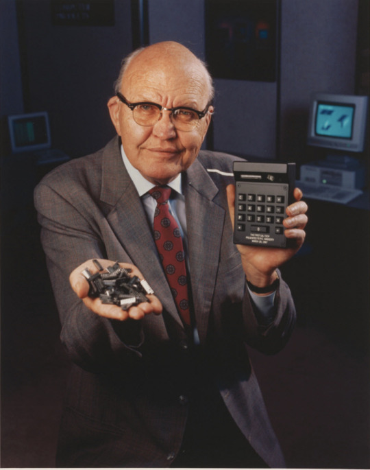
Jack Kilby (8 November 1923 – 20 June 2005)
Kilby was hired by Texas Instruments in May 1958 to work on miniaturization. By July, Kilby thought he had come up with a solution. Rather than creating individual circuit components from various materials and then wiring them together onto a non-conductive base, the components and the base could all be made out of a single piece of semiconductor material, an integrated circuit.
Robert Noyce was working on the same issue at the same time at the Schockley Semiconductor Laboratory and is credited with inventing a more practical version than Kilby (Kilby mentioned Noyce 3 times in his Nobel Prize acceptance speech in 2000).
Kilby would go on to develop the pocket calculator, the first consumer product built using integrated circuits.
6 notes
·
View notes
Text

The factories that make chips are expensive AF — many billions of dollars — but the process isn’t expensive to run at scale. It’s a little bit like silkscreening t-shirts, in multiple color layers, only shrunk way down and the “ink” is applied by light through tiny masks. Each printed wafer is then cut apart into hundreds of chips.
When people came up with this process in the 1960s, it was low-resolution and the details (transistors) were visible to the naked eye. Since then it’s been a process of iteration where people keep refining the techniques and, about every 18 months, retool or rebuild the factories to make chips with everything half the size as before. That’s where Moore's Law comes from.
“SCIENCE: IT WORKS, BITCHES” —xkcd
Have you ever wondered how tech technicians recover data from faulty flash and memory whose data cannot be recovered by normal methods.
55K notes
·
View notes
Text
Express Technology Group: Leading the Charge in Integrated Circuit Solutions for Advanced Manufacturing and Engineering Needs
Express Technology Group is revolutionizing integrated circuit solutions for advanced manufacturing and engineering. With cutting-edge products and reliable service, they provide businesses with the essential components to optimize performance, enhance innovation, and meet the demands of modern industries.
0 notes
Text
Why does digital elecronics is important for engineering?
Digital electronics is super important in engineering for a bunch of reasons—it's pretty much the backbone of modern technology. Digital electronics powers everything from smartphones and computers to cars and medical devices. Engineers across disciplines need to understand it to design, troubleshoot, or innovate with modern systems.

Digital systems work with binary signals (0s and 1s), Less sensitive to noise and signal degradation. Easier to design for precise and repeatable performance.

GET CIRCUIT DESIGNING VIDEO TUTORIAL 👈.
#crank shaft#engine mechanism#four stroke engine#mechanical arms#mechanical engineering#mechanical parts#two stroke engine#digital electronics#digital circuit#digital circuit design#iot circuits#integrated circuits#embeddedsystems#embedded circuit#embedded systems
0 notes
Video
chips by Francois Flibotte Via Flickr: Detailed view of a printed circuit board (PCB), showcasing its complex electronic components and their interconnections. The image focuses on surface-mount devices (SMDs) and other electronic parts soldered to the PCB, revealing its intricate design and functionality.
#capacitors#circuit board#connectors#electronic components#hardware#integrated circuits#resistors#surface-mount devices#Montreal#Quebec#Canada#flickr
0 notes
Text

Fabrication of functional 3D multi-level microstructures on transparent substrates by one step back-side UV photolithography (Kang, Myeongwoo & Byun, Jae & Na, Sangcheol & Jeon, Noo. (2017). RSC Adv.. 7. 13353-13361. 10.1039/C6RA28812J.)
#science#engineering#photolithography#integrated circuits#electronics#physics#circuits#computers#technology
21 notes
·
View notes
Text
VNI4140K Specifications & Features Explained
The VNI4140K is a cutting-edge high-side smart power switch designed for industrial and automotive applications. But what makes it special? Why should engineers and tech enthusiasts care about it? This article dives deep into its specifications, features, and applications, making it easy to understand—even for those unfamiliar with complex electronic components.
What is the VNI4140K?
The VNI4140K is an intelligent quad high-side power switch designed to handle loads with enhanced safety and efficiency. It integrates various protection features, making it ideal for automotive, industrial, and smart control applications.
Key Features of the VNI4140K
Quad-channel high-side switch
Over-temperature protection
Short-circuit protection
Overvoltage clamp
Low power consumption
Diagnostic feedback for fault detection
Technical Specifications
Operating Voltage: 8V – 36V
Maximum Load Current: 2A per channel
On-Resistance (Rds ON): 0.1Ω (typical)
ESD Protection: Yes (IEC 61000-4-2 compliant)
Temperature Range: -40°C to 150°C
Package: PowerSSO-36
Pin Configuration and Functions
The VNI4140K comes in a PowerSSO-36 package with dedicated input, output, and diagnostic pins. Key pins include:
VCC: Power supply input
IN1-IN4: Control inputs
OUT1-OUT4: Output channels
GND: Ground
FAULT: Diagnostic feedback
How the VNI4140K Works
The VNI4140K acts as a smart electronic switch, replacing traditional mechanical relays. It uses MOSFET technology to efficiently control high-current loads while offering built-in safety features. The fault diagnostics system detects and prevents issues like overheating or short circuits.
Advantages Over Traditional Switches
Improved Energy Efficiency: Consumes less power compared to mechanical relays.
Enhanced Durability: Solid-state design minimizes wear and tear.
Faster Response Time: Reacts quicker to input signals.
Integrated Protection Features: Prevents circuit damage due to overcurrent or overheating.
Common Applications
The VNI4140K is widely used in:
Automotive electronics (lighting systems, door locks)
Industrial automation (motor controls, PLCs)
Smart home devices (intelligent power management)
Medical equipment (precision switching for diagnostics and monitoring devices)
Installation and Usage Guidelines
Ensure proper heat dissipation to prevent overheating.
Connect the diagnostic pin to a microcontroller for real-time monitoring.
Use appropriate filtering capacitors to stabilize the power supply.
Avoid exceeding maximum load limits to prevent system failure.
Troubleshooting and Maintenance Tips
Overheating? Ensure proper ventilation and heat sinks.
No output signal? Check control input voltage.
Short circuit detected? Inspect load connections and wiring.
Intermittent operation? Test for voltage fluctuations.
Conclusion
The VNI4140K is a powerful and reliable quad high-side smart switch designed for various industrial and automotive applications. With advanced protection features, low power consumption, and efficient performance, it offers significant advantages over traditional switching solutions. Whether you're an engineer or a tech enthusiast, understanding its specifications and features can help you integrate it effectively into your designs.
0 notes
Text
How Electronic Integrated Circuits Revolutionized Technology
Technology has been revolutionized by the development of smaller, faster, and more efficient devices, thanks to Electronic Integrated Circuits (ICs). Shenzhen Informic Electronic Limited offers high-quality ICs that power innovative solutions, driving advancements across various industries.
#electronics#integratedcircuit#branding#marketing#ecommerce#integrated circuits#electronic components#electronic#china
0 notes
Text
Un día como hoy (5 de diciembre) en la tecnología

El 5 de diciembre de 1957 el ingeniero suizo-americano, Jean Hoerni, presenta el proceso planar, que se convirtió en fundamental en la fabricación de circuitos integrados #retrocomputingmx #integratedcircuit #jeanhoerni
0 notes
Text
What is a Field-Effect Transistor?
A Field-Effect Transistor is a three-terminal device that controls current flow through a semiconductor by using an electric field. It consists of three electrodes: the Source, Drain, and Gate. By applying a voltage to the gate, the conductivity of the semiconductor channel can be changed, thereby controlling the current between the source and drain.
Get more details: What is a Field-Effect Transistor?
#electronics#integrated circuits#semiconductor#components#electronic#module#chips#electronic devices#manufacturing#transistors
0 notes