#sram chip programming
Explore tagged Tumblr posts
Visit Tumblr Blog
Explore Tumblr blogs with no restrictions, modern design and the best experience.
Last Seen Tumblr Blogs


Fun Fact
1,644 Tumblr posts in 1 second.
Text
Memory ICs, SRAM memory chips, SRAM chip programming, SRAM interface
CY62157E Series 8 Mb (512 K x 16) 4.5 - 5.5 V 45 ns Static RAM - TSOP-44
0 notes
Text
https://www.futureelectronics.com/p/semiconductors--memory--RAM--nvram--quantum-trap-nvsram/m95m02-drmn6tp-stmicroelectronics-3034532
Non-volatile memory, SRAM data, SRAM chip programming, Non volatile memory
M95M02 Series 2 Mb (256 K x 8) 5.5 V Serial SPI Bus EEPROM - SOIC-8
#RAM#NVRAM#Nonvolatile SRAM (NVSRAM)#M95M02-DRMN6TP#STMicroelectronics#memory#data#SRAM chip programming#card#Random Access Memory#flip-flop circuit#SRAM application#what is SRAM#SRAM application system#chips#SRAM
1 note
·
View note
Text
https://www.futureelectronics.com/p/semiconductors--memory--RAM--nvram--quantum-trap-nvsram/mx29f040cqi-70g-macronix-6159320
Static random access memory, types of volatile memory, sram programming
MX29F Series 4-Mbit (512 K x 8) 70 ns 5 V Surface Mount Flash Memory - PLCC-32
#Macronix#MX29F040CQI-70G#RAM#NVRAM#Nonvolatile#SRAM (NVSRAM)#SRAM solutions#sram memory#Ram digital#card#static random access memory#types of volatile memory#sram chip programming#Static RAM (SRAM)#sram memory chips
1 note
·
View note
Text
https://www.futureelectronics.com/p/semiconductors--memory--RAM--static-ram--asynchronous/cy62157ev18ll-55bvxi-infineon-3728565
SRAM memory cell, Types of SRAM, data Memory, memory card reader
CY62157EV18 Series 8 Mb (512 K x 16) 1.65 - 2.25 V 55 ns Static RAM - VFBGA-48
#RAM#Static RAM#Asynchronous SRAM#CY62157EV18LL-55BVXI#Infineon#memory cell#Types of SRAM#data#card reader#programming#Random Access Memory#SRAM chip#flash memory card reader#Nv SRAM#SRAM memory#CMOS Static RAM
1 note
·
View note
Text
https://www.futureelectronics.com/p/semiconductors--memory--RAM--static-ram--asynchronous/cy62167ev30ll-45bvxi-infineon-6042923
Non-Volatile SRAM memory, Non-Volatile SRAM, Non volatile memory
CY62167EV30 Series 16 Mb (1M x 16/2M x 8) 2.2 - 3.6 V 45 ns Static RAM -TSOP-48
#RAM#Static RAM#Asynchronous SRAM#CY62167EV30LL-45ZXIT#Infineon#Non-Volatile SRAM memory#Non-Volatile SRAM#Surface Mount Flash Memory#Memory chips#Random-Access Memory#Volatile Memory#Programming System Devices
1 note
·
View note
Text
https://www.futureelectronics.com/p/semiconductors--memory--RAM--static-ram--asynchronous/cy62167ev30ll-45bvxit-infineon-1068579
Non Volatile SRAM memory, What is SRAM, SRAM manufacturers, SRAM chip
CY62167EV30 Series 16 Mb (1M x 16 / 2 M x 8) 3 V 45 ns Static RAM - FBGA-48
#RAM#Static RAM Asynchronous#SRAM#CY62167EV30LL-45BVXIT#Infineon#Non Volatile SRAM memory#What is SRAM#manufacturers#SRAM ram chip#Static random access memory#SRAM memories#Memory Density#Programming System Devices
1 note
·
View note
Text
https://www.futureelectronics.com/p/semiconductors--memory--RAM--nvram--quantum-trap-nvsram/m95m02-drmn6tp-stmicroelectronics-8011669
Static ram manufacturers, Battery backed Static RAM, SRAM memory card
M95M02 Series 2 Mb (256 K x 8) 5.5 V Serial SPI Bus EEPROM - SOIC-8
#STMicroelectronics#M95M02-DRMN6TP#RAM#NVRAM#Nonvolatile SRAM (NVSRAM)#Static ram manufacturers#Battery backed Static RAM#SRAM memory card#SRAM programming#Memory ICs#SRAM manufacturers#Random Access Memory#SRAM memory chips#SRAM chip
1 note
·
View note
Text
https://www.futureelectronics.com/p/semiconductors--memory--RAM--nvram--quantum-trap-nvsram/m95m02-drmn6tp-stmicroelectronics-7140290
SRAM chip, SRAM memory card, SRAM memory chips, static random access memory
M95M02 Series 2 Mb (256 K x 8) 5.5 V Serial SPI Bus EEPROM - SOIC-8
#RAM#NVRAM#Nonvolatile SRAM (NVSRAM)#M95M02-DRMN6TP#STMicroelectronics#Ram digital#what is SRAM#non volatile SRAM#static RAM#SRAM chip#card#static random-access memory#RAM digital to analog converter#SRAM programming
1 note
·
View note
Text
SRAM chip, SRAM programming, non volatile static ram, SRAM manufacturers
AS6C62256 Series 256-kbit (32 K x 8) 3.3 V 55 ns CMOS Static RAM - PDIP-28
0 notes
Text
https://www.futureelectronics.com/p/semiconductors--memory--RAM--nvram--quantum-trap-nvsram/m95m02-drmn6tp-stmicroelectronics-3034532
EPROM, FIFO's, Flash Memory, what is SRAM, Static RAM, SRAM transmission
M95M02 Series 2 Mb (256 K x 8) 5.5 V Serial SPI Bus EEPROM - SOIC-8
#RAM#NVRAM#Nonvolatile SRAM (NVSRAM)#M95M02-DRMN6TP#STMicroelectronics#Dual port memory#what is a dual port SRAM#Battery Backed SRAM#Dual Port Memory#EPROM#FIFO's#Flash Memory#Static RAM#transmission#Battery backed Static RAM#chip programming
1 note
·
View note
Note
What are some of the coolest computer chips ever, in your opinion?
Hmm. There are a lot of chips, and a lot of different things you could call a Computer Chip. Here's a few that come to mind as "interesting" or "important", or, if I can figure out what that means, "cool".
If your favourite chip is not on here honestly it probably deserves to be and I either forgot or I classified it more under "general IC's" instead of "computer chips" (e.g. 555, LM, 4000, 7000 series chips, those last three each capable of filling a book on their own). The 6502 is not here because I do not know much about the 6502, I was neither an Apple nor a BBC Micro type of kid. I am also not 70 years old so as much as I love the DEC Alphas, I have never so much as breathed on one.
Disclaimer for writing this mostly out of my head and/or ass at one in the morning, do not use any of this as a source in an argument without checking.
Intel 3101
So I mean, obvious shout, the Intel 3101, a 64-bit chip from 1969, and Intel's first ever product. You may look at that, and go, "wow, 64-bit computing in 1969? That's really early" and I will laugh heartily and say no, that's not 64-bit computing, that is 64 bits of SRAM memory.
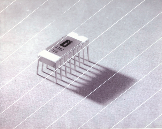

This one is cool because it's cute. Look at that. This thing was completely hand-designed by engineers drawing the shapes of transistor gates on sheets of overhead transparency and exposing pieces of crudely spun silicon to light in a """"cleanroom"""" that would cause most modern fab equipment to swoon like a delicate Victorian lady. Semiconductor manufacturing was maturing at this point but a fab still had more in common with a darkroom for film development than with the mega expensive building sized machines we use today.
As that link above notes, these things were really rough and tumble, and designs were being updated on the scale of weeks as Intel learned, well, how to make chips at an industrial scale. They weren't the first company to do this, in the 60's you could run a chip fab out of a sufficiently well sealed garage, but they were busy building the background that would lead to the next sixty years.
Lisp Chips
This is a family of utterly bullshit prototype processors that failed to be born in the whirlwind days of AI research in the 70's and 80's.
Lisps, a very old but exceedingly clever family of functional programming languages, were the language of choice for AI research at the time. Lisp compilers and interpreters had all sorts of tricks for compiling Lisp down to instructions, and also the hardware was frequently being built by the AI researchers themselves with explicit aims to run Lisp better.
The illogical conclusion of this was attempts to implement Lisp right in silicon, no translation layer.
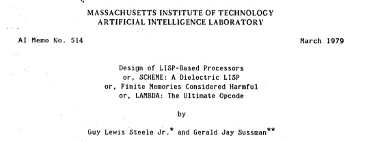
Yeah, that is Sussman himself on this paper.
These never left labs, there have since been dozens of abortive attempts to make Lisp Chips happen because the idea is so extremely attractive to a certain kind of programmer, the most recent big one being a pile of weird designd aimed to run OpenGenera. I bet you there are no less than four members of r/lisp who have bought an Icestick FPGA in the past year with the explicit goal of writing their own Lisp Chip. It will fail, because this is a terrible idea, but damn if it isn't cool.
There were many more chips that bridged this gap, stuff designed by or for Symbolics (like the Ivory series of chips or the 3600) to go into their Lisp machines that exploited the up and coming fields of microcode optimization to improve Lisp performance, but sadly there are no known working true Lisp Chips in the wild.
Zilog Z80
Perhaps the most important chip that ever just kinda hung out. The Z80 was almost, almost the basis of The Future. The Z80 is bizzare. It is a software compatible clone of the Intel 8080, which is to say that it has the same instructions implemented in a completely different way.
This is, a strange choice, but it was the right one somehow because through the 80's and 90's practically every single piece of technology made in Japan contained at least one, maybe two Z80's even if there was no readily apparent reason why it should have one (or two). I will defer to Cathode Ray Dude here: What follows is a joke, but only barely

The Z80 is the basis of the MSX, the IBM PC of Japan, which was produced through a system of hardware and software licensing to third party manufacturers by Microsoft of Japan which was exactly as confusing as it sounds. The result is that the Z80, originally intended for embedded applications, ended up forming the basis of an entire alternate branch of the PC family tree.
It is important to note that the Z80 is boring. It is a normal-ass chip but it just so happens that it ended up being the focal point of like a dozen different industries all looking for a cheap, easy to program chip they could shove into Appliances.
Effectively everything that happened to the Intel 8080 happened to the Z80 and then some. Black market clones, reverse engineered Soviet compatibles, licensed second party manufacturers, hundreds of semi-compatible bastard half-sisters made by anyone with a fab, used in everything from toys to industrial machinery, still persisting to this day as an embedded processor that is probably powering something near you quietly and without much fuss. If you have one of those old TI-86 calculators, that's a Z80. Oh also a horrible hybrid Z80/8080 from Sharp powered the original Game Boy.
I was going to try and find a picture of a Z80 by just searching for it and look at this mess! There's so many of these things.
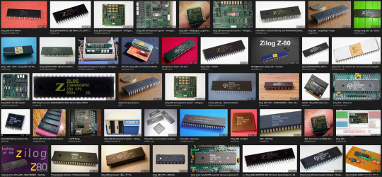
I mean the C/PM computers. The ZX Spectrum, I almost forgot that one! I can keep making this list go! So many bits of the Tech Explosion of the 80's and 90's are powered by the Z80. I was not joking when I said that you sometimes found more than one Z80 in a single computer because you might use one Z80 to run the computer and another Z80 to run a specialty peripheral like a video toaster or music synthesizer. Everyone imaginable has had their hand on the Z80 ball at some point in time or another. Z80 based devices probably launched several dozen hardware companies that persist to this day and I have no idea which ones because there were so goddamn many.
The Z80 eventually got super efficient due to process shrinks so it turns up in weird laptops and handhelds! Zilog and the Z80 persist to this day like some kind of crocodile beast, you can go to RS components and buy a brand new piece of Z80 silicon clocked at 20MHz. There's probably a couple in a car somewhere near you.
Pentium (P6 microarchitecture)
Yeah I am going to bring up the Hackers chip. The Pentium P6 series is currently remembered for being the chip that Acidburn geeks out over in Hackers (1995) instead of making out with her boyfriend, but it is actually noteworthy IMO for being one of the first mainstream chips to start pulling serious tricks on the system running it.

The P6 microarchitecture comes out swinging with like four or five tricks to get around the numerous problems with x86 and deploys them all at once. It has superscalar pipelining, it has a RISC microcode, it has branch prediction, it has a bunch of zany mathematical optimizations, none of these are new per se but this is the first time you're really seeing them all at once on a chip that was going into PC's.
Without these improvements it's possible Intel would have been beaten out by one of its competitors, maybe Power or SPARC or whatever you call the thing that runs on the Motorola 68k. Hell even MIPS could have beaten the ageing cancerous mistake that was x86. But by discovering the power of lying to the computer, Intel managed to speed up x86 by implementing it in a sensible instruction set in the background, allowing them to do all the same clever pipelining and optimization that was happening with RISC without having to give up their stranglehold on the desktop market. Without the P5 we live in a very, very different world from a computer hardware perspective.
From this falls many of the bizzare microcode execution bugs that plague modern computers, because when you're doing your optimization on the fly in chip with a second, smaller unix hidden inside your processor eventually you're not going to be cryptographically secure.
RISC is very clearly better for, most things. You can find papers stating this as far back as the 70's, when they start doing pipelining for the first time and are like "you know pipelining is a lot easier if you have a few small instructions instead of ten thousand massive ones.
x86 only persists to this day because Intel cemented their lead and they happened to use x86. True RISC cuts out the middleman of hyperoptimizing microcode on the chip, but if you can't do that because you've girlbossed too close to the sun as Intel had in the late 80's you have to do something.
The Future
This gets us to like the year 2000. I have more chips I find interesting or cool, although from here it's mostly microcontrollers in part because from here it gets pretty monotonous because Intel basically wins for a while. I might pick that up later. Also if this post gets any longer it'll be annoying to scroll past. Here is a sample from a post I have in my drafts since May:
I have some notes on the weirdo PowerPC stuff that shows up here it's mostly interesting because of where it goes, not what it is. A lot of it ends up in games consoles. Some of it goes into mainframes. There is some of it in space. Really got around, PowerPC did.
237 notes
·
View notes
Text
PiSquare: RP2040 & ESP-12E-based board for all Raspberry Pi HATs
PiSquare is a compact, wireless communication board designed for Raspberry Pi that enables you to wirelessly connect and communicate with multiple Raspberry Pi HATs including SPI, I2C, and SPI HATs. It is based on two powerful components:
⦁ The RP2040 microcontroller (the same chip used in the Raspberry Pi Pico). ⦁ The ESP-12E Wi-Fi module for seamless wireless communication.
By using socket programming, PiSquare can wirelessly interact with Raspberry Pi HATs through TCP/IP communication, allowing you to connect as many devices as you need, without worrying about physical stacking or GPIO conflicts.
Key Specifications:
⦁ Microcontroller: Raspberry Pi RP2040
Core Architecture: Dual-core ARM Cortex-M0+ microcontroller
Clock Speed: Up to 133 MHz
Flash Memory: 2MB onboard QSPI Flash (for program storage)
RAM: 264KB SRAM
GPIO Pins: 26 multi-function GPIO pins with support for PWM, SPI, I2C, UART, and other peripherals
⦁ Wi-Fi Connectivity: ESP-12E
Wi-Fi Standard: 802.11 b/g/n
Wireless Frequency: 2.4 GHz
Wi-Fi Chipset: ESP8266 (with 4MB of onboard Flash)
Data Rate: Up to 72.2 Mbps (with 802.11n support)
Communication Interface: UART (Universal Asynchronous Receiver Transmitter)
⦁ Wireless Communication via Socket Programming
Protocol: TCP/IP (Transmission Control Protocol/Internet Protocol) via socket programming
Connection Type: Full-duplex, bi-directional communication
Network Type: Local Area Network (LAN) or Wi-Fi based network for device communication
Number of Supported Devices: Configurable for communication with multiple (n) Raspberry Pi HATs over Wi-Fi without the need for physical stacking
Socket Layer: Raw socket-based communication for sending and receiving data over the network
⦁ HAT Compatibility
Supported Protocols: SPI (Serial Peripheral Interface): Full-duplex, synchronous communication for connecting peripherals
I2C (Inter-Integrated Circuit): Multi-master, multi-slave communication for sensors, actuators, and peripheral devices
GPIO-based HATs: Supports a variety of devices and sensors with GPIO pin control
Pin Multiplexing: Flexible I/O pin assignment allowing for easy configuration of multiple communication protocols simultaneously
Addressing: Supports unique addressing for SPI and I2C devices to avoid conflicts
⦁ Power Supply
Voltage: 5V DC ±5% (typical operating voltage range)
Power Consumption: Low-power operation suitable for remote or battery-powered applications
Regulation: Onboard linear voltage regulator to provide stable power for the microcontroller and Wi-Fi module
⦁ Form Factor
Dimensions: 65mm x 30mm x 20mm (compact design suitable for integration into small devices)
Mounting: Compatible with standard Raspberry Pi connectors (via external interface) without the need for physical GPIO stacking
⦁ I/O and Expansion
Interface: UART, SPI, I2C (for communication with external peripherals)
GPIO: 26 GPIO pins for signal input/output, including support for digital, analog, PWM, and interrupts
Use Cases
Here are a few ways PiSquare can revolutionize your Raspberry Pi projects:
Multi-HAT Robotics: Easily connect multiple HATs for motor control, sensor arrays, and communication modules in a wireless setup.
IoT Projects: PiSquare can communicate with several sensor HATs in remote locations, sending data back to a central Raspberry Pi for processing or cloud storage.
Home Automation: Connect a variety of home automation HATs wirelessly, creating a smart home system that’s efficient and scalable.
Distributed Sensor Networks: Set up multiple sensors across a large area without worrying about physical connections or pin conflicts.
The Pisquare RP2040 with the onboard ESP-12E Wi-Fi module is a powerful and compact solution for anyone looking to build wireless IoT projects. Its support for multiple HATs, including SPI and I2C, makes it versatile enough to handle a wide variety of peripherals, while its ability to implement socket programming provides you with the flexibility to create robust networked applications.
Whether you're creating a smart home system, an industrial IoT device, or a robotics project, the Pisquare by SB Components can be the perfect foundation for your next creation.
#technology#raspberry pi#innovation#tech#techinnovation#programming#tech projects#projects#artificial intelligence#technews
0 notes

Text
The Future of AI is Here: Cerebras' WSE-2 is the largest computer chip ever built and the fastest AI processor on Earth
See on Scoop.it - Design, Science and Technology
Cluster-Scale Performance on a Single Large-Wafer Chip
Video is here
Programming a cluster to scale deep learning is painful. It typically requires dozens to hundreds of engineering hours and remains a practical barrier for many to realize the value of large-scale AI for their work. On a traditional GPU cluster, ML researchers – typically using a special version of their ML framework – must figure out how to distribute their model while still achieving some fraction of their convergence and performance target. They must navigate the complex hierarchy of individual processors’ memory capacity, bandwidth, interconnect topology, and synchronization; all while performing a myriad of hyper-parameter and tuning experiments along the way. What’s worse is that the resultant implementation is brittle to change, and this time only delays overall time to solution. With the WSE, there is no bottleneck. We give you a cluster-scale AI compute resource with the programming ease of a single desktop machine using stock TensorFlow or PyTorch. Spend your time in AI discovery, not cluster engineering.
Learn more
Designed for AI
Each core on the WSE is independently programmable and optimized for the tensor-based, sparse linear algebra operations that underpin neural network training and inference for deep learning, enabling it to deliver maximum performance, efficiency, and flexibility. The WSE-2 packs 850,000 of these cores onto a single processor. With that, and any data scientist can run state-of-the-art AI models and explore innovative algorithmic techniques at record speed and scale, without ever touching distributed scaling complexities.
1000x Memory Capacity and Bandwidth
Unlike traditional devices, in which the working cache memory is tiny, the WSE-2 takes 40GB of super-fast on-chip SRAM and spreads it evenly across the entire surface of the chip. This gives every core single-clock-cycle access to fast memory at extremely high bandwidth – 20 PB/s. This is 1,000x more capacity and 9,800x greater bandwidth than the leading GPU. This means no trade-off is required. You can run large, state-of-the art models and real-world datasets entirely on a single chip. Minimize wall clock training time and achieve real-time inference within latency budgets, even for large models and datasets.
220Pb/s
High Bandwidth - Low Latency
Deep learning requires massive communication bandwidth between the layers of a neural network. The WSE uses an innovative high bandwidth, low latency communication fabric that connects processing elements on the wafer at tremendous speed and power efficiency. Dataflow traffic patterns between cores and across the wafer are fully configurable in software. The WSE-2 on-wafer interconnect eliminates the communication slowdown and inefficiencies of connecting hundreds of small devices via wires and cables. It delivers an incredible 220 Pb/s processor-processor interconnect bandwidth. That’s more than 45,000x the bandwidth delivered between graphics processors.
Read the full article at: www.cerebras.net
0 notes
Text
LIERDA OCB ANTENNA MODULE
LSD4BT-K55 Module
K55 BLE mesh Standard Module (PCB Antenna)
K55 series of low-power Bluetooth module is a high-performance Bluetooth module which is developed based on the Telink low-power Bluetooth SoC TLSR8250 chip. The module adopts the stamp- type and side plug-in interfaces, is exquisite and compact, is fully lead out via ports and convenient to use, and helps the users omit the complicated RF hardware design, development and production links. Therefore, the users can easily realize the development of Bluetooth application programs on that basis, shorten the R&D cycle, and seize the market opportunities. This model is a pure hardware module that excludes any software. If you need the edition with software, please notify in advance.
Key Benefits
Parameter
·Working Frequency Band
-Working frequency band: 2402-2480MHz
·Ultra-low Power Consumption
-Support 1.8V-3.6V powersupply
-Emission current: ≤20mA (10dBm power
configuration)
-Receiving current: ≤6.5mA (overall current)
-Sleep current: 400nA (SRAM notsaving)
·High-link Budget
-Sensitivity-96dBm±1dBm (1Mbps, PER<30.8%)
-Emission power: Max.10dBm
·Memory Resources
-Internal 512kB Flash (the capacity that
the client can actually use is less than
512kB)
-48kB on-chip SRAM, wherein 32kB can sleep and save
·Compatibility
-Designed interface mode with side
plug-in and stamp holes compatible
·Mesh Functions
-Support BLE
-Support the Bluetooth SIG Mesh
-Support the exclusive Mesh of Telink·Communication Interface
-5 PWM / 16 GPIO / 1 UART(Pin
multiplexing)
Application
PC, Tablet, Mobile Phone, Handheld, and Other Low-Power Peripheral Devices
Smart Household Appliances
Smart City
For more information please visit: https://en.lierda.com/
Hope to be your valued supplier from China. CONTACT: AMINA ZHU E MAIL: [email protected] WhatsApp: 008615061516896 https://en.lierda.com/
youtube
IoTembedded #microcontrollers #sensors #wirelesscommunication #IoTgateways #IoTcloudplatforms #embeddedmicro-controltechnology #RFhardwareR&D #5Gcommunicationsolution #NB-loT #LoRa #Wi-Fi #Wi-SUN #BLE #IOTsystem #semiconductordistribution #cloudpipe-endsolutions #Cat.1 #Wi-SUN #ZigBee #AIrecognition #IoTbasicservice
#IoT
#InternetofThings
0 notes
Text
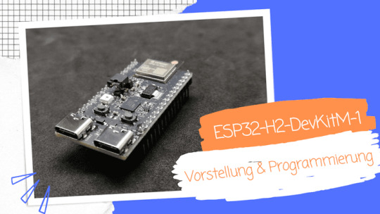
Mikrocontroller ESP32 H2 im Test

In diesem Beitrag möchte ich dir den Mikrocontroller ESP32 H2 vorstellen und diesen auch mit anderen baugleichen Mikrocontrollern der ESP32 Reihe vergleichen.
Der Mikrocontroller wurde das erste Mal von Espressif auf der Seite https://www.espressif.com/en/news/ESP32_H2 im August 2021 angepriesen. Das Releasedate ist jedoch immer wieder bedingt durch die Covid Pandemie verschoben worden und liegt nun auf das erste Quartal 2023 und somit konnte ich mir eines dieser Geräte ergattern.
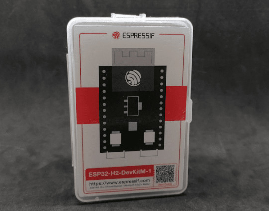
ESP32 H2 kaufen
Den Mikrocontroller bekommst du derzeit für knapp 16 € zzgl. Versandkosten auf aliexpress.com.

ESP32 H2 auf aliexpress.com Das ist für einen ESP32 nicht gerade günstig, aber gemessen an den Features (werde ich im nächsten Kapitel aufzeigen) finde ich den Preis angemessen.

Features des ESP32 H2
Besonders zu nennen ist, dass der Mikrocontroller als "Zigbee-konforme Plattform" zertifiziert und eine "Thread-zertifizierte 1.3.0-Komponente" ist. Des Weiteren wird Bluetooth 5.2 (LE) & IEEE 802.15.4 unterstützt, somit ist dieser Mikrocontroller bestens für deine Low Energy Projekte im Bereich IoT geeignet. Der ESP32-H2 macht es einfacher, sichere Geräte zu bauen. Er hat viele Funktionen, die sicherstellen, dass die Daten sicher sind, wie z.B. das sichere Booten, die Flash-Verschlüsselung und digitale Signaturen. Auch die Identität des Geräts ist geschützt. All diese Funktionen machen den Mikrocontroller erschwinglich und geben dem Benutzer die Sicherheit, dass seine Daten geschützt sind.
Technische Daten
Hier nun die, wie ich finde, technischen Daten des Mikrocontrollers: Chipsingle core, 32-bit RISC-VTaktfrequenz160 MHzSpeicher128 KB ROM 320 KB SRAM 4 KB LP Speicher 2 MB oder 4MB SiP Flash SpeicherSchnittstellen2x USB-Typ-C 2.0, SPI, UART, I2C, I2CBluetooth 5.2 Low Energy, IEEE 802.15.4, Zigbee & ThreadGPIOs19 frei programmierbare GPIOsTechnische Daten des ESP32-H2 Dies ist nur ein kleiner Auszug aus den technischen Daten, welche du komplett als PDF Dokument unter https://cdn-shop.adafruit.com/product-files/5715/esp32-h2_datasheet_en.pdf findest.
Pinout & Aufbau
Was als Erstes auffällt ist, dass der Mikrocontroller zwei USB-C Schnittstellen hat. Des Weiteren verfügt dieser auf der Vorder- und Rückseite über Pinbeschriftungen.

Mikrocontroller - ESP32-H2-DevKitM-1
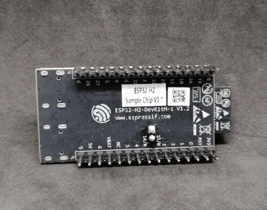
Mikrocontroller - ESP32-H2-DevKitM-1 (Rückseite) Auf der Vorderseite finden wir einen RGB NeoPixel sowie zwei Taster Boot & Reset. Über den Jumper J5 kannst du die Stromaufnahme des Mikrocontrollers messen, hier musst du den Jumper entfernen und ein Strommessgerät in Reihe schalten.
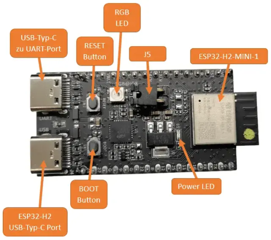
Aufbau des ESP32-H2 DevKitM-1
Anschluss an den PC
Wenn du dein USB-Typ-C Kabel in den mit USB beschrifteten Anschluss mit dem PC verbindest dann wird dieses Gerät als "Serielles USB-Gerät" erkannt. Am Anschluss UART wird das Gerät als "Silicon Labs CP210x USB to UART Bridge" erkannt.


Programmieren in der Arduino IDE
Den Mikrocontroller kannst du derzeit (Stand 25.05.2023) nicht in der Arduino IDE 2.0 programmieren. Der ESP32 wird zwar erkannt aber leider nicht korrekt.

Arduino IDE 2.0 - Mikrocontroller ESP32-H2-DevKitM-1 als ESP32-S3 erkannt Wenn wir nun einen Code hochladen dann erhalten wir die Ausgabe vom esptool.py das der gewählte Chip nicht passt. Sketch uses 257969 bytes (19%) of program storage space. Maximum is 1310720 bytes. Global variables use 19496 bytes (5%) of dynamic memory, leaving 308184 bytes for local variables. Maximum is 327680 bytes. esptool.py v4.5.1 Serial port COM4 Connecting... A fatal error occurred: This chip is ESP32-H2 not ESP32-S3. Wrong --chip argument? Auch ein Update des Boardtreibers auf die Version 2.0.9 bringt derzeit nicht den passenden Treiber mit und daher bleibt derzeit nur die Wahl zur Espressif IDE. Du bekommst jedoch für Eclipse & VSCode ein passendes Plugin welches du installieren kannst und dann deinen Mikrocontroller über diese IDE programmieren kannst. Wie du das machst erfährst du demnächst auf meinem Blog! Read the full article
0 notes