#wireless RF circuit
Explore tagged Tumblr posts
Visit Tumblr Blog
Explore Tumblr blogs with no restrictions, modern design and the best experience.
Last Seen Tumblr Blogs


Fun Fact
Tumblr has a low social media market share in South America.
Text
https://www.futureelectronics.com/p/semiconductors--wireless-rf--receiver-ics/clrc63201t-0fe-112-nxp-2283646
NXP, CLRC63201T/0FE,112, Wireless & RF Receiver ICs
CLRC632 Series Multiple Protocol Contactless Reader IC (MIFARE/I-CODE1) -SOIC-32
#NXP#CLRC63201T/0FE#112#Wireless & RF Receiver ICs#HDMI circuit#wireless RF circuit#RF radio frequency#AM FM receiver#HDMI receiver IR circuit#Phase locked loop#what is a FM receiver circuit#Phase lock loops#wireless Bluetooth receiver
2 notes
·
View notes
Text
High performance circuit, High speed data transmission, module bluetooth
SP3077E Series 16 Mbps ±15 kV ESD Protected RS-485/RS-422 Transceiver-NSOIC-8
#MaxLinear#SP3077EEN-L#Wireless & RF#Transceiver ICs#RF Transceiver utilizes#band signals#wireless transmitter#Wifi#Bluetooth transceiver#usb wireless transceiver#High performance circuit#High speed data transmission#module
1 note
·
View note
Text
Wireless rf frequency, digital audio mixer circuit programming, RFID capability
NT3H2111 Series 3.6 V 13.56 MHz Surface Mount RFID Transponder - XQFN-8
#Wireless & RF#RF Modules & Solutions RFID#NT3H2111W0FHKH#NXP#Wireless rf frequency#digital audio mixer circuit programming#RFID capability#rf control systems#Wireless detectors circuit#remote control#Digital rf modulator#demodulator
1 note
·
View note
Text
High speed data, rf module, rf transmitter, receiver module transceiver circuit
SP3072 Series 0.25 Mbps 3.3 V Half-Duplex SMT RS 485 Transceiver - SOIC-8N
#Wireless & RF#Transceiver ICs#SP3072EEN-L#MaxLinear#High speed data#rf module#rf transmitter#circuit#usb wireless transceiver#Bluetooth transceiver#high performance circuit#Microwave transceiver#WIFI#transceiver circuit
1 note
·
View note
Text
Best Partner for Wireless Modules: A Comprehensive Antenna Selection Guide
n the field of wireless communication, antenna selection is crucial. It not only affects the coverage range and transmission quality of signals but also directly relates to the overall performance of the system. Among various wireless modules, finding the right antenna can maximize their potential, ensuring stable and efficient data transmission.
When designing wireless transceiver devices for RF systems, antenna design and selection are essential components. A high-quality antenna system can ensure optimal communication distances. Typically, the size of antennas of the same type is proportional to the wavelength of the RF signal; as signal strength increases, the number of required antennas also grows.
Antennae can be categorized as internal or external based on their installation location. Internal antennas are installed within the device, while external antennas are mounted outside.
In situations where space is limited or there are multiple frequency bands, antenna design becomes more complex. External antennas are usually standard products, allowing users to simply select the required frequency band without needing additional tuning, making them convenient and easy to use.
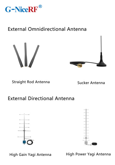
What are the main types of antennas?
External Antennas: These antennas can be classified into omnidirectional antennas and directional antennas based on the radiation pattern.
Internal Antennas: These antennas refer to antennas that can be placed inside devices.
Omnidirectional Antennas: These antennas radiate signals uniformly in the horizontal plane, making them suitable for applications that require 360-degree coverage, such as home Wi-Fi routers and mobile devices.
Directional Antennas: These antennas have a high emission and reception strength in one or more specific directions, while the strength is minimal or zero in others. Directional antennas are primarily used to enhance signal strength and improve interference resistance.
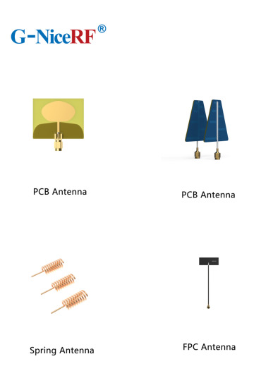
PCB Antennas: These antennas are directly printed on the circuit board and are suitable for devices with limited space, commonly used in small wireless modules and IoT devices.
FPC Antennas: FPC antennas are flexible printed circuit antennas that are lightweight, efficient, and easy to integrate.
Concealed Antennas: Designed for aesthetic purposes, concealed antennas can be hidden within devices or disguised as other objects, making them suitable for applications where appearance is important without compromising signal quality.
Antenna Selection Guide
When selecting the appropriate antenna for a communication module, it's essential to first determine whether to use an internal or external antenna based on the module's structure.
External Antennas: These antennas offer high gain, are less affected by the environment, and can save development time, but they may take up space and impact the product's aesthetics.
Internal Antennas: These have relatively high gain and are installed within the device, maintaining a clean and appealing exterior.
Sucker Antennas: These provide high gain and are easy to install and secure.
Copper Rod Sucker Antennas: Made from large-diameter pure copper radiators, these are highly efficient with a wide bandwidth.
Rubber Rod Antennas: Offer moderate gain at a low cost.
Fiberglass Antennas: Suitable for harsh environments and ideal for long-distance signal

External Directional Antennas
Typically used in environments with long communication distances, small signal coverage areas, and high target density.
Panel Antennas have high efficiency, are compact, and easy to install, while considering the impact of gain and radiation area Yagi Antennas offer very high gain, are slightly larger, and have strong directionality, making them suitable for long-distance signal transmission; however, attention must be paid to the antenna's orientation during use
Internal Antenna Selection
Most internal antennas are affected by environmental factors and may require custom design or impedance matching
Spring Antennas are cost-effective but have low gain and narrow bandwidth, often requiring tuning for good matching when installed Ceramic Patch Antennas occupy minimal space and perform well, but have a narrow bandwidth
For details, please click:https://www.nicerf.com/products/ Or click:https://nicerf.en.alibaba.com/productlist.html?spm=a2700.shop_index.88.4.1fec2b006JKUsd For consultation, please contact NiceRF (Email: [email protected]).
2 notes
·
View notes
Text
Robust Growth Forecast for Global RF Chip Inductor Market Through 2031
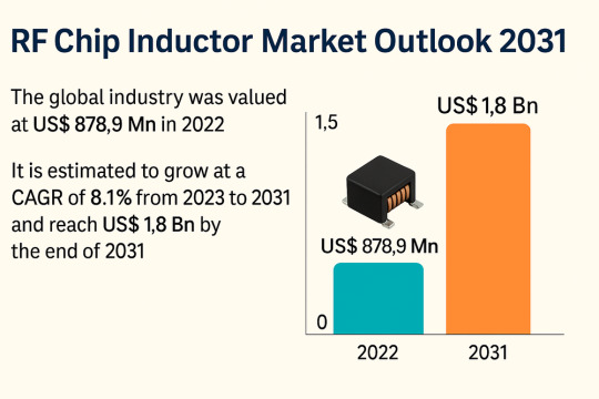
The global RF chip inductor market, valued at US$ 878.9 Mn in 2022, is projected to reach US$ 1.8 Bn by 2031, expanding at a CAGR of 8.1% from 2023 to 2031. Driven by rapid advancements in wireless communication, miniaturization of electronic devices, and increased integration of RF components in automobiles, the market is poised for robust growth throughout the forecast period.
Market Overview: RF chip inductors are integral components in wireless systems, designed for use in compact electronic circuits to manage radio frequency (RF) signals. These inductors are commonly integrated into System-on-Chip (SoC) and Integrated Circuit (IC) applications across smartphones, laptops, automotive electronics, and Internet of Things (IoT) devices.
Ceramic and ferrite types dominate the RF chip inductor market, with ceramic variants gaining significant traction due to their high-Q factors and low losses.
Market Drivers & Trends
1. Proliferation of Wireless Devices The surge in global demand for smartphones, tablets, smartwatches, and wireless earphones has led to a parallel rise in demand for RF chip inductors. These components are essential for wireless signal tuning and filtering, enabling efficient data transmission.
2. Automotive Electronics Boom Modern vehicles are evolving into connected hubs with built-in infotainment, GPS, keyless entry, and telematics systems. RF chip inductors are critical to these systems, especially in enabling secure and efficient data communication. India’s vehicle exports exceeding 5.6 million units in 2022 underscore the automotive sector's expanding role.
3. Government Investments Strategic investments in telecommunications infrastructure, like India's US$ 611.1 Mn for BharatNet, bolster the deployment of RF components, accelerating market growth.
Latest Market Trends
Miniaturization and Material Innovation Key industry players are focused on innovating smaller form factor inductors that can perform at higher frequencies. Advanced material research is helping improve signal integrity and reduce power consumption.
Rise of Wearables and IoT RF chip inductors are becoming central to the performance of wearable technologies, enabling seamless Bluetooth and Wi-Fi connectivity.
Increased Demand for Ceramic Inductors Ceramic chip inductors, which held a 54.3% share in 2022, offer superior performance, particularly in high-frequency environments. This segment is expected to grow at 8.4% CAGR during the forecast period.
Key Players and Industry Leaders
The global RF chip inductor industry is moderately consolidated with major players driving technological advancements through R&D and strategic partnerships. Leading companies include:
Murata Manufacturing Co., Ltd.
Coilcraft Inc.
KYOCERA AVX Components Corporation
Vishay Intertechnology, Inc.
Johanson Technology Incorporated
Würth Elektronik GmbH & Co. KG
Viking Tech Corporation
These companies are investing in ceramic and multilayer inductor technologies, launching ultra-miniature and high-performance products.
Access important conclusions and data points from our Report in this sample - https://www.transparencymarketresearch.com/sample/sample.php?flag=S&rep_id=85752
Recent Developments
Gowanda Electronics (Feb 2022) launched the SMP0603 ceramic chip inductors, targeting power and RF applications in automotive and industrial systems.
KYOCERA AVX (Mar 2021) introduced the LCCI series multilayer ceramic chip inductors, designed for compact mobile and wireless systems including RFID, WLAN, and EMI suppression in high-frequency circuits.
Market Opportunities
Emerging Markets Rapid urbanization and rising digital connectivity in developing countries, particularly in Asia Pacific and Latin America, present significant growth potential.
5G Rollout The global deployment of 5G networks will further increase the demand for high-performance RF chip inductors, especially those that can handle ultra-high frequencies.
Electric and Autonomous Vehicles The transition toward autonomous and electric vehicles is expected to significantly boost demand for compact and robust RF components, opening lucrative avenues for market expansion.
Future Outlook
The RF chip inductor market is projected to continue its upward trajectory due to:
Expansion in consumer electronics production
Innovation in inductor materials and manufacturing
Strategic alliances and mergers among major players
Growing application in healthcare and industrial IoT
By 2031, the market is expected to nearly double in size, creating opportunities across the value chain, from component design and production to system integration.
Market Segmentation
By Type
Ceramic
Ferrite
By Structure Type
Film
Wire Wound
Multilayer
Air Core
By Inductance Range
Up to 100 nH
100–200 nH
200–400 nH
400–800 nH
800 nH–3.3 µH
Above 3.3 µH
By Application
Infotainment Systems
Smartphones
Portable Electronics
Broadband
Computer Peripherals
RFIDs
RF Transceivers
Others (Medical Imaging, PCS Modules)
By End-use Industry
Automotive & Transportation
Aerospace & Defense
Consumer Electronics
IT & Telecommunications
Industrial
Others (Healthcare, Energy, etc.)
Regional Insights
Asia Pacific leads the global RF chip inductor market, holding 40.8% market share in 2022. It is projected to maintain dominance due to:
High concentration of consumer electronics manufacturers
Growth in automotive production and export
Expansion of 5G infrastructure, especially in China, Japan, and South Korea
North America accounted for 27.6% market share in 2022 and is likely to experience steady growth due to advanced R&D capabilities and adoption of high-frequency RF applications in aerospace and defense.
Europe is also a promising region, especially with increasing focus on electric mobility and connected car infrastructure.
Why Buy This Report?
Comprehensive Market Coverage: Includes quantitative and qualitative analysis from 2017 to 2031.
In-depth Segmentation: Extensive breakdown by type, application, structure, and region.
Company Profiles: Detailed insights into major players and their strategic developments.
Industry Analysis: Includes Porter’s Five Forces, value chain analysis, and market attractiveness.
Actionable Insights: Identify key opportunities, regional hotspots, and emerging applications.
Explore Latest Research Reports by Transparency Market Research: Semiconductor Etching Equipment Market: https://www.transparencymarketresearch.com/semiconductor-etching-equipment-market.html
Linear Motor Market: https://www.transparencymarketresearch.com/linear-motor-market.html
Wafer Handling Robots Market: https://www.transparencymarketresearch.com/wafer-handling-robots-market.html
Time of Flight Sensor Market: https://www.transparencymarketresearch.com/time-of-flight-sensor-market.html
0 notes
Text
Strategies for Reducing the Amount of EMFs in Your Home

In the last few years, electromagnetic frequencies (EMFs) have become a concern for many in a world where EMFs are integral to communications and energy. EMF refers to the radiation emitted every time you use an electronic device, whether a computer, a microwave, a cell phone, or power your home with electricity. In high amounts, EMFs can affect your health. However, you can reduce EMF levels in your home in several ways.
To begin with, there are four types of EMFs: magnetic fields, electric fields, radio frequencies (RFs), and finally, so-called “dirty electricity”.
Reducing the amount of EMFs in your home starts with purchasing one or more EMF meters. They give you readings of magnetic fields, electric fields, micro/radio waves and dirty electricity where you sit, sleep and stand. These meters can tell you the level of magnetic fields emitted from your appliances and devices and the level of RF from your cell phone, tablet or laptop and from nearby cell phone towers in the neighborhood.
We protect against magnetic field EMFs by choosing houses away from power lines that generate magnetic fields into the yard and house (however not all power lines emit magnetic fields that reach the house). We can hire a building biologist to work with an electrician to trace and fix wiring errors in electrical circuits. Go to https://buildingbiologyinstitute.org/find-an-expert/ to find a building biologist near you. A plumber can insert a dielectric union into your incoming metal water pipe from the city water main under the street if the incoming pipe carries electric current as that pipe runs under your floor, which is another source of magnetic fields.
You can also reduce magnetic field EMF exposure by sitting, sleeping and standing more than six feet from a breaker panel or refrigerator and replacing electricity-operated appliances with battery-operated ones, such as the clock next to your bed.
Reducing electric field EMF levels in your home can be as simple as turning off circuit breakers that power circuits to your bedrooms at night. A building biologist can determine which circuits need to be shut off. An electrician can install a U.L.-approved remote circuit cut off kit next to your panel so that you can remotely shut off circuits at night when you sleep from your bedroom without having to go to the breaker panel.
Finally, to reduce daytime electric field EMFs, make sure your computer has a grounded power supply with a three-pronged plug, especially laptops. Read the Electric Field section of Safer Use of Computers for details at https://createhealthyhomes.com/education/safer-use-of-computers/.
Tamping down technology use can reduce radiofrequency EMFs. Experts recommend reducing use of cell phones when away from home, increasing the distance between the phone and your head and body, and favoring hardwired connections when at home, in the office and at school (then put the device in Airplane Mode with WiFi and Bluetooth “Off”). Hardwire your laptop’s connection to the Internet with a grounded, shielded Ethernet cable. See Safer Use of Computers (https://createhealthyhomes.com/education/safer-use-of-computers/) and Safer Use of Cell Phones (https://createhealthyhomes.com/education/safer-use-of-cell-phones/).
Another suggestion is to stop using Bluetooth headphones, which emit high radio frequency levels. Consider alternatives to Bluetooth headsets, such as wired or air tube headphones, which emit 99 percent less RF than traditional headphones. Air tube headphones produce sound through hollow tubes, which bring sound from the device to your ear without carrying wireless RF radiation that is transmitted from the phone’s antenna up the wire all the way to your head.
We recommend that you avoid sleeping next to your cell phone. Experts state that sleeping beside your phone or with it under your pillow is the worst thing you can do to reduce radio frequency exposure. If you use your cell phone alarm to wake up, experts recommend putting your cell phone into Airplane Mode when sleeping (making sure WiFi and Bluetooth are “Off”) or switching altogether to a battery-operated alarm clock and charging your cell phone in another room.
Dirty electricity, the fourth type of EMF, radiates into rooms from high-frequency voltage spikes carried on electrical circuits and plugged-in cords. The sources of theses spikes of dirty power can be mini-split air conditioning units, energy-efficient furnaces, smart home devices, and other appliances that generate electrical interference that is then carried on and radiated from circuits and cords in your house and in your neighbor’s houses. Other seemingly innocuous sources of dirty power are LED and fluorescent lights (including those with dimmers), solar panel inverters, smart electric meters, variable speed motors in appliances, switch-mode electronic power supplies, cell phone chargers and adapters, and energy-efficient appliances.
Dirty electricity has negative impacts on human health, including depression, fatigue, and cancer. High levels of dirty power can interfere with the nervous, immune, and circulatory systems.
You should consider switching out your compact fluorescent light (CFL) bulbs, which generate high amounts of dirty electricity—high-frequency electricity lights the gas in the bulbs, unlike standard 60 Hertz. While CFLs are more efficient than older incandescent light bulbs, they create electrical spikes on wiring in your house. Instead of using CFLs, consider purchasing incandescent light bulbs where they are available, or LEDs, which now have less dirty electricity than they used to. Look for brands that have low flicker, available from the Flicker Alliance (https://flickeralliance.org/collections/flicker-free-light-bulbs) and the Light Bulb Database (https://optimizeyourbiology.com/light-bulb-database).
Dimmer switches enable you to control how bright the lights are in a room through a knob or slider you can adjust. However, dimmer switches can only work by turning the electricity flow off and on thousands of times each second. The lower the light level, the more the voltage on the line is broken up. Ultimately, this contributes counter-intuitively to higher dirty power generation. Avoid dimmers if you are sensitive to dirty electricity.
Oram Miller is a BBEC, EMRS, Certified Building Biology Environmental Consultant, Electromagnetic Radiation Specialist and Healthy New Building and Remodeling Consultant.
0 notes
Text
CMOS Power Amplifiers Market Drivers Enhancing Efficiency, Integration, and Cost-Effective Wireless Communication Solutions
The CMOS power amplifiers market is witnessing a steady growth trajectory driven by multiple technological, commercial, and application-oriented factors. With wireless communication becoming more pervasive and devices getting smaller and smarter, the demand for compact, energy-efficient, and cost-effective power amplification solutions has risen sharply. CMOS (Complementary Metal-Oxide-Semiconductor) technology, traditionally known for its applications in microprocessors and memory chips, has increasingly found a strong foothold in RF (Radio Frequency) front-end modules, especially power amplifiers.

Rising Demand for Wireless Connectivity
One of the key market drivers is the explosive growth in wireless communication technologies, including 4G, 5G, Wi-Fi 6, and the upcoming 6G. These technologies demand highly efficient and reliable RF components. CMOS power amplifiers provide a suitable balance of performance and affordability, making them ideal for use in smartphones, tablets, IoT devices, wearables, and connected home solutions. As more industries adopt wireless systems for communication, automation, and control, the reliance on CMOS amplifiers continues to expand.
Integration with System-on-Chip (SoC) Solutions
CMOS technology enables easy integration of power amplifiers with digital and analog circuits on the same die, a key driver pushing its adoption in consumer electronics and mobile devices. System-on-Chip integration reduces component count, lowers power consumption, and enables the development of ultra-compact devices. Manufacturers prefer CMOS PAs because of their scalability and compatibility with large-scale semiconductor manufacturing processes, leading to economies of scale and reduced production costs.
Cost Efficiency and Mass Production Benefits
Another important market driver is the cost-effectiveness of CMOS technology. Unlike GaAs (Gallium Arsenide) or other compound semiconductor-based amplifiers, CMOS-based designs are more suitable for high-volume, low-cost manufacturing. This makes them ideal for mass-market applications like smartphones and IoT sensors, where price sensitivity is critical. The use of CMOS also simplifies the supply chain and shortens development cycles, encouraging faster time-to-market for OEMs.
Expansion of IoT and Smart Devices
The rapid growth of the Internet of Things (IoT) ecosystem is a significant catalyst for the CMOS power amplifiers market. Billions of devices—from smart meters and industrial sensors to home automation systems and connected healthcare devices—require efficient RF amplification. CMOS power amplifiers meet the low power, small form factor, and cost demands of such devices, making them an indispensable component in this domain. The proliferation of IoT across both industrial and consumer landscapes ensures long-term demand for CMOS PAs.
Evolution of 5G and Future Networks
As the world shifts toward 5G and beyond, there is an increasing need for high-speed, high-frequency data transmission. Although early 5G implementations relied heavily on GaN and GaAs technologies for their high power capabilities, CMOS-based amplifiers are becoming viable alternatives in specific frequency bands and low-power use cases. The need for a large number of small cell deployments and low-power devices for edge communication is boosting CMOS PA adoption.
Emphasis on Power Efficiency and Battery Life
In mobile and wearable devices, power consumption is a critical factor. CMOS power amplifiers offer better power efficiency at lower costs, helping extend battery life while maintaining signal integrity. As consumers demand longer battery runtime and more powerful features in compact devices, the adoption of CMOS PAs becomes a strategic necessity for device manufacturers.
Growth in Automotive and Industrial Applications
Automotive electronics and industrial automation are increasingly incorporating wireless modules for connectivity and control. From advanced driver-assistance systems (ADAS) to vehicle-to-everything (V2X) communication, these systems benefit from the integration capabilities and robustness of CMOS power amplifiers. Similarly, in industrial automation and remote monitoring, the ability to have low-cost, power-efficient communication modules is pushing the use of CMOS-based RF components.
Government Support and Technological Advancements
Government policies promoting 5G infrastructure, digital transformation, and Industry 4.0 are encouraging the deployment of advanced communication networks that rely on CMOS-based power amplifier technologies. At the same time, advancements in CMOS fabrication and design techniques have helped close the performance gap between CMOS and traditional compound semiconductor technologies. Innovations such as envelope tracking, digital predistortion, and linearization techniques are helping CMOS amplifiers achieve better performance metrics, including linearity and efficiency.
Conclusion
The CMOS power amplifiers market is being driven by a confluence of technological advancements and application needs. As the global economy becomes increasingly digital and wireless-dependent, the demand for scalable, cost-effective, and power-efficient amplification solutions will continue to grow. CMOS power amplifiers, with their integration capability, cost benefits, and evolving performance levels, are well-positioned to address the diverse needs of consumer electronics, automotive, industrial, and telecom sectors.
0 notes
Text
What is copper clad steel wire used for
Copper clad steel wire (CCS) is a composite material that combines the strength of steel with the electrical conductivity of copper. Manufactured by bonding a copper layer onto a steel core through electroplating, cladding, or other metallurgical processes, CCS offers a cost-effective alternative to pure copper conductors while maintaining critical performance characteristics. This article explores the diverse applications of copper clad steel wire across industries, highlighting its role in modern technology and infrastructure.
Telecommunications and Cable Industries CCS is widely used in telecommunications, particularly in coaxial cables for cable TV (CATV) subscriber lines and broadband networks. Its ability to leverage the "skin effect"—a phenomenon where high-frequency signals travel primarily along the conductor's surface—allows CCS to match the conductivity of pure copper at frequencies above 5 MHz. This makes it ideal for inner conductors in coaxial cables, where copper ensures signal integrity while steel provides mechanical strength. For instance, Shanghai BISCO International Corporation’s CCS products, compliant with standards like ASTM B227 and GB 12269, are deployed in CATV systems and local area networks (LANs), offering durability and cost efficiency.
Electrical Power Transmission and Grounding In the power sector, CCS serves as a reliable conductor for overhead transmission lines, grounding systems, and railway electrification. Its high tensile strength, derived from the steel core, enables it to withstand mechanical stress in long-span installations. Meanwhile, the copper layer ensures low electrical resistance, critical for efficient power transfer. CCS is also used in grounding rods for electrical installations, where its corrosion resistance—enhanced by surface treatments like tin or silver plating—extends service life. For example, Jiangsu Reliable Industry Co., Ltd. produces CCS wires with conductivities ranging from 21% to 40% IACS, suitable for power transmission and grounding applications.
Electronics and Component Manufacturing CCS wire is a preferred material for electronic components, such as connectors, leads, and printed circuit board (PCB) traces. The copper layer provides solderability and electrical conductivity, while the steel core adds structural rigidity. This combination is valuable in high-density electronics, where space constraints demand materials that balance performance and mechanical integrity. Additionally, CCS is used in RF (radio frequency) cables for high-frequency applications, such as antennas and wireless communication systems, where its skin-effect properties ensure minimal signal loss.
Railway and Transportation Infrastructure The transportation sector relies on CCS for catenary wires in electrified railways and tram systems. Here, the material’s strength-to-weight ratio is crucial for supporting overhead lines over long distances. For example, Japan’s Shinkansen bullet trains use CCS catenary wires to ensure reliable power delivery at high speeds. CCS is also employed in grounding systems for railway infrastructure, protecting against lightning strikes and electrical faults.
Defense and Aerospace Applications In defense and aerospace, CCS is used for lightweight, high-strength wiring in aircraft, satellites, and military equipment. Its resistance to vibration and extreme temperatures makes it suitable for avionics systems, where reliability is non-negotiable. Additionally, CCS is used in shielded cables to protect sensitive electronics from electromagnetic interference (EMI).
Renewable Energy and High-Temperature Systems CCS is gaining traction in renewable energy projects, such as solar farms and wind turbines, where its durability and conductivity are valued in harsh environments. It is also used in high-temperature applications, such as industrial furnaces and heating elements, where copper’s thermal conductivity and steel’s heat resistance are synergistic.
Conclusion Copper clad steel wire (CCS) has emerged as a versatile material with applications spanning telecommunications, power transmission, electronics, transportation, defense, and renewable energy. Its unique combination of steel’s mechanical strength and copper’s electrical conductivity makes it indispensable in industries where performance, cost, and durability are critical. As technology advances, CCS continues to evolve, with new specifications (e.g., ASTM’s proposed 21–70% IACS standards) expanding its potential in emerging fields. Whether in high-frequency cables, railway catenaries, or aerospace wiring, CCS remains a testament to the power of composite materials in modern engineering. Its adaptability and reliability ensure that copper clad steel wire will remain a cornerstone of infrastructure and technology for years to come.
0 notes
Text
Antenna in Package AiP Market Opportunities Rising with Expansion of Millimeter Wave Technology Globally
The Antenna in Package (AiP) market is gaining significant traction as wireless communication technologies become increasingly integrated into compact, high-performance electronic devices. AiP technology incorporates antennas directly into semiconductor packages, enabling advanced radio frequency (RF) performance while saving space. This innovation is particularly relevant in 5G, millimeter-wave (mmWave), automotive radar, satellite communications, and IoT applications.

Market Drivers
One of the primary drivers of the AiP market is the global rollout of 5G technology, which operates at higher frequencies such as mmWave. These frequencies require advanced antenna solutions capable of handling high data rates and low latency. Traditional printed circuit board (PCB) antennas often fall short in terms of integration and performance. AiP offers a more efficient alternative by reducing interconnect losses and supporting beamforming technologies critical for 5G.
Another major factor is the increasing miniaturization of consumer electronics. Smartphones, wearables, and IoT devices demand compact components that deliver excellent performance. AiP technology meets this requirement by integrating the antenna and RF front-end into a single compact module, freeing up space and improving system-level efficiency.
Technological Advancements
Recent advancements in substrate materials, system-in-package (SiP) technologies, and 3D packaging are making AiP solutions more cost-effective and scalable. Low-temperature co-fired ceramic (LTCC) and organic substrates have enabled better thermal and electrical performance. Integration of multiple functions such as filters, power amplifiers, and transceivers within the package has allowed manufacturers to create multi-functional modules tailored for specific end-uses.
In addition, the evolution of advanced simulation tools and design automation has shortened development cycles and reduced costs, making AiP more accessible to a broader range of industries. These advancements have facilitated faster prototyping and more reliable testing environments.
Key Market Segments
The AiP market can be segmented based on frequency band, end-user application, and geography.
By frequency, the market includes sub-6 GHz and mmWave segments, with mmWave seeing higher growth due to its necessity in 5G and automotive radar applications.
By application, the market is divided into consumer electronics, automotive, telecommunications, aerospace and defense, and industrial IoT.
Geographically, North America and Asia-Pacific dominate the AiP landscape, thanks to the presence of major semiconductor companies and 5G infrastructure deployment.
Regional Insights
Asia-Pacific leads the AiP market due to robust electronics manufacturing ecosystems in countries like China, South Korea, Taiwan, and Japan. Government initiatives to boost 5G and smart city projects further support AiP growth in the region. North America, especially the United States, sees significant demand from telecom providers, defense contractors, and autonomous vehicle manufacturers. Europe is also emerging as a key region, driven by automotive and industrial automation applications.
Competitive Landscape
The AiP market is highly competitive, with key players including Qualcomm, ASE Group, Amkor Technology, Murata Manufacturing, TSMC, and MediaTek. These companies are investing in research and development to improve integration, reduce power consumption, and enhance RF performance. Collaborations, joint ventures, and strategic acquisitions are common strategies to gain market share and accelerate product development.
Startups and mid-sized players are also entering the space with niche AiP solutions for IoT and wearable devices, contributing to market dynamism and innovation.
Challenges and Opportunities
Despite its promise, AiP adoption faces several challenges. High design complexity, thermal management issues, and initial manufacturing costs are significant barriers. Additionally, maintaining signal integrity in densely packed modules remains a technical hurdle.
However, opportunities abound. As mmWave adoption expands and edge computing grows in importance, AiP is poised to play a pivotal role in enabling low-latency, high-speed communication across various devices and systems. The trend toward smart cities, connected vehicles, and AR/VR applications also offers long-term growth potential.
Future Outlook
The AiP market is expected to grow at a CAGR exceeding 15% over the next five years, driven by surging demand across multiple industries. Technological advancements, cost optimization, and expanding 5G infrastructure will be key enablers. As device manufacturers strive to balance performance, size, and power efficiency, AiP is likely to become a standard in RF design and packaging.
#AntennaInPackage#AiPMarket#5GTechnology#MillimeterWave#WirelessCommunication#IoTDevices#RFTechnology
0 notes
Text
B.Tech in Electronics and Communication Engineering: A Comprehensive Guide for Aspiring Engineers
Are you passionate about technology, communication systems, and electronics? A Bachelor of Technology (B.Tech) in Electronics and Communication Engineering (ECE) offers a dynamic and future-ready career path. This program integrates core principles of electronics with modern communication technologies, preparing students for diverse roles in today's tech-driven world.
Understanding Electronics and Communication Engineering
Electronics and Communication Engineering is a discipline that combines electronic engineering with computer science and information technology. It focuses on designing, developing, and testing electronic circuits, devices, and communication equipment like transmitters, receivers, and integrated circuits. This field is pivotal in the advancement of technologies such as mobile phones, satellite systems, and the Internet of Things (IoT).
Course Structure and Curriculum
The B.Tech ECE program typically spans four years, divided into eight semesters. The curriculum is designed to provide a strong foundation in both theoretical and practical aspects of electronics and communication.
Core Subjects:
Digital Electronics
Analog Circuits
Signals and Systems
Electromagnetic Field Theory
Microprocessors and Microcontrollers
Communication Systems
VLSI Design
Embedded Systems
Wireless Communication
Optical Communication
Laboratory Work:
Hands-on experience is a crucial part of the program, with labs focusing on circuit design, signal processing, microprocessor programming, and communication systems.
Electives and Specializations:
Students can choose electives in areas like:
Artificial Intelligence and Machine Learning
Internet of Things (IoT)
Robotics
Nanotechnology
Biomedical Engineering
Eligibility and Admission Process
To enroll in a B.Tech ECE program, candidates must meet the following criteria:
Educational Qualification: Completion of 10+2 with Physics, Chemistry, and Mathematics as core subjects.
Minimum Marks: A minimum aggregate score of 50-60% in the qualifying examination (may vary by institution).
Entrance Exams: Qualifying scores in entrance exams like JEE Main, state-level CETs, or institution-specific tests.
Career Opportunities After B.Tech ECE
Graduates of ECE have a plethora of career options across various industries.
Job Roles:
Electronics Engineer
Communication Engineer
Embedded Systems Developer
Network Engineer
VLSI Design Engineer
IoT Developer
RF Engineer
R&D Engineer
Industries:
Telecommunications
Consumer Electronics
Automotive
Aerospace
Healthcare Technology
Defense and Military
Information Technology
Higher Studies:
Graduates can pursue M.Tech, MBA, or research programs in specialized fields to enhance their knowledge and career prospects.
Top Electronics and Communication Engineering Colleges in Pune
Pune is home to several esteemed institutions offering B.Tech in ECE:
DES Pune University
MIT World Peace University (MIT-WPU)
Vishwakarma Institute of Information Technology
Dr. D. Y. Patil Institute of Technology
Bharati Vidyapeeth Deemed University College of Engineering
PES Modern College of Engineering
These colleges are known for their robust curriculum, experienced faculty, and excellent placement records.
Why Choose DES Pune University for B.Tech ECE?
At DES Pune University, the B.Tech in Electronics and Communication Engineering program is meticulously designed to align with industry standards and technological advancements. The university offers:
Comprehensive Curriculum: Integrating core ECE subjects with emerging technologies.
State-of-the-Art Laboratories: Equipped with modern tools and equipment for practical learning.
Experienced Faculty: A team of dedicated educators and industry professionals.
Industry Collaborations: Partnerships with leading companies for internships and projects.
Placement Support: Dedicated cell to assist students in securing employment opportunities.
Choosing DES Pune University ensures a holistic education experience, preparing students to excel in the ever-evolving field of electronics and communication engineering.
Embark on a journey of innovation and technology with a B.Tech in Electronics and Communication Engineering. Equip yourself with the skills and knowledge to shape the future of communication and electronic systems.
0 notes
Text
The UFL Male PCB Mount SMT Connector is a small, surface-mount RF connector engineered for high-frequency signal transmission. It is particularly suitable for applications with limited space, supporting a 50-ohm impedance and frequently utilized in wireless modules, antennas, and GPS devices. This connector guarantees dependable, low-loss connections on printed circuit boards.
0 notes
Text
On September 28, Boao Forum for Asia (BFA) held the Second Conference of International Science, Technology and Innovation Forum (ISTIF). As a major forum of the conference this year, the session “5G Application and 6G Prospect” was successfully held.
The session was hosted by Guoqing Hu, head of the 5G group at Peking University Shenzhen Research Institute and director of Guangdong Institute of Frontier Science and Technology. Six experts from leading enterprises, universities and research institutes in communications, through online and offline interaction, discussed the current status of research and development of key 5G hardware and software technologies and the future outlook of 6G development. The experts made their contribution to the "Boao wisdom" regarding accelerating the digital transformation and upgrading of traditional industries based on 5G and opening up the era of the digital economy.
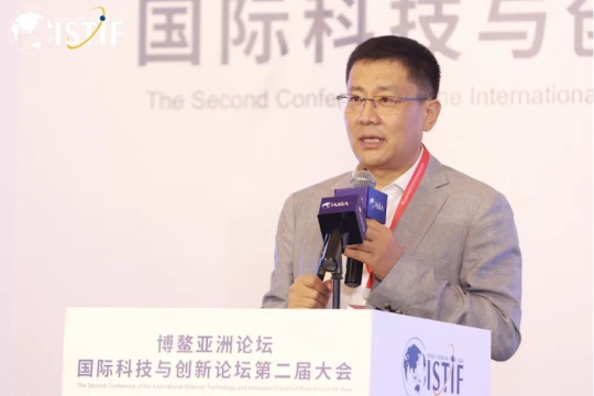
Quan Xue
Quan Xue, Dean of the School of Electronics and Information Engineering of the South China University of Technology, introduced the research results of the South China University of Technology in both millimetre wave integrated circuits and antennas with the theme of "millimetre wave antennas and integrated circuits in 5G/6G mobile communications". He delivered expectations on the application of these research results that can be implemented in future communication systems.

Tianhai Chang
Tianhai Chang, Chief Architect of Huawei Access Network, delivered a speech on "FTTR Leads F5G, Creates New Hundred Billion Industry". According to Chang, FTTR (Fiber to the Room) is the second all-optical revolution for homes and buildings after the FTTx primary optical reform, which is the upgrade of the home network industry and technology. As a result, home broadband is moving towards a new era of experience, which breeds huge business opportunities. There are great technological innovation opportunities in C-WAN network architecture, RF and antenna, communication algorithms, artificial intelligence, etc. FTTR will not only be a new blue ocean for industry, but also for academic innovation.

Xiangyang Duan
Xiangyang Duan, Vice President and General Manager of Wireless Architecture of Zhongxing Telecom Equipment, elaborated on the 5G-enabled industry and 6G continuous innovation. He pointed out that the current application of 5G in various industries is at the edge of the period from exploration to an explosion. This period requires continuous innovation in mobile communication technologies and solutions, and continuous iteration with a deeper understanding of the industry as well as industry needs and applications. At the same time, he proposed that 6G is likely to be the scenario for the smart connection of everything and he with his team will continue to investigate with 6G as the target.

Lili Tan
Lili Tan, General Manager of the Product R&D Center of China Mobile Group Guangdong Company, introduced the overall situation of Guangdong Mobile’’s 5G digital intelligence technology to help the development of Guangdong Hong Kong Macao Greater Bay Area. She depicted the blueprint of 5G-6G technology research and industry application development with the “New Three”, that is, "new trend, new momentum, new outlook". Tan believed that the only constant in the continuous development of technology will be the win-win cooperation, so CMGD will enhance cooperation, effective linkage and a winning future with the government units in charge, both the upstream and downstream industry chains, research institutes and other related organizations.
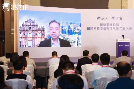
Chengbin Yu
Chengbin Yu, Member of the Macao Committee for the Guangdong-Hong Kong-Macao Greater Bay Area Development, Member of the Institute of Electrical and Electronics Engineers, also the Chairman of the Founding Institute of Industrial Technology of Macau, shared his view on "5G industry lights up the digital future - analogue technology breaks through the bottleneck of core creation". Yu believed that 5G and 6G mark a leap from the interconnection of everything to the smart connection of everything. They are the further expansion from serving people and things to supporting the efficient interconnection of intelligent bodies and will also be the link between the real physical world and the virtual digital world, thus improving the quality of life and promoting the development of social transformation.

Fusheng Zheng
Fusheng Zheng, President of Guangdong New Generation Communications & Networks Innovation Institute, delivered a speech on "A fully distributed network architecture for 5G-A/6G with air-space integration". Zheng pointed out that with the further development of 5G, various industries have put forward higher demands on the future 5G-A/6G network architecture, including higher reliability, lower latency, and ubiquitous connectivity across space and time. By constructing a fully distributed and diffuse fog core network, the network layers will be greatly simplified and break through the key bottlenecks of architecture latency, reliability, scalability and diversity in traditional mobile Internet. As a result, it will better enable typical scenarios such as high-mobility telematics, immersive telemedicine and satellite internet.
0 notes
Text
CHIP Ceramic Patch Antenna vs. Bluetooth Patch Antenna: Which Is More Suitable for Your Device?
In wireless communication device design, antenna selection directly impacts signal transmission quality, device size, and user experience. With the rapid development of fields like the Internet of Things (IoT) and smart wearables, CHIP ceramic patch antennas and Bluetooth patch antennas have become mainstream choices due to their distinct characteristics.

I. Antenna Basics: CHIP Ceramic Patch Antenna vs. Bluetooth Patch Antenna
1. CHIP Ceramic Patch Antenna
Principle and Structure:Utilizes ceramic materials (such as dielectric ceramics) as the substrate, achieving signal transmission and reception through microstrip or radiation patch designs. The high dielectric constant of ceramics allows the antenna to operate at smaller sizes, suitable for high-frequency applications (e.g., 2.4GHz, 5GHz).
Core Advantages:
Multi-Band Compatibility: Supports Wi-Fi, Bluetooth, Zigbee, and other protocols, reducing the number of antennas within a device.
Strong Environmental Resistance: Ceramic material is resistant to high temperatures and corrosion, making it suitable for industrial or outdoor scenarios.
High Signal Purity: Low-loss characteristics reduce signal interference, enhancing transmission stability.
2. Bluetooth Patch Antenna
Principle and Structure:Specifically designed for the Bluetooth frequency band (2.4GHz-2.485GHz), typically using PCB substrates or flexible materials. The structure is simple, and the cost is relatively low.
Core Advantages:
Extreme Miniaturization: Sizes can be as small as 3×1.5mm, suitable for miniature devices (e.g., TWS earbuds).
Low Power Consumption Optimization: Designed for Bluetooth Low Energy (BLE) protocols, extending battery life.
Rapid Integration: No complex matching circuits required, simplifying the development process.
II. Key Comparisons: Which Is More Suitable for Your Device?
Comparison DimensionCHIP Ceramic Patch AntennaBluetooth Patch AntennaApplicable Frequency BandsMulti-band (Wi-Fi/Bluetooth/Zigbee, etc.)Single Bluetooth bandSizeRelatively larger (considering ceramic substrate thickness)Extremely small (suitable for space-constrained devices)CostHigher (due to material and process complexity)Lower (standardized design)Environmental AdaptabilityExcellent (resistant to high temperatures, vibrations)General (depends on PCB protection)Typical ApplicationsSmart home gateways, industrial sensors, smartwatchesBluetooth earbuds, smart tags, medical wearables
Scenario-Based Selection Recommendations
Need Multi-Protocol Support? Choose CHIP Ceramic Patch AntennaFor example, smart home central control devices need to connect to both Wi-Fi and Bluetooth. The multi-band characteristics of ceramic antennas can reduce the number of antennas, optimizing layout.
Kinghelm Case: Their KH-CPA series ceramic antennas support dual-band (2.4GHz/5GHz), applied in smart speakers, enhancing signal coverage by 20%.
Pursuing Extreme Miniaturization? Choose Bluetooth Patch AntennaFor instance, TWS earbuds have limited internal space, making the miniature design of Bluetooth patch antennas an ideal choice.
Kinghelm Case: The KH-BTA series patch antennas measure only 3.2×1.6mm, enabling a brand's earbuds to achieve stable transmission over 10 meters.
Operating in Harsh Environments? Choose Ceramic AntennaIndustrial equipment operating in high-temperature or vibration environments benefits from the high reliability of ceramic materials.
Kinghelm Technical Highlight: Achieved AEC-Q200 automotive-grade certification, withstanding temperatures ranging from -40℃ to 125℃.
III. Kinghelm Solutions: Technology and Services
As a leading domestic supplier of microwave RF antennas, Kinghelm Electronics offers customized antenna solutions for various scenarios:
1. CHIP Ceramic Patch Antenna
KH-CPA Series:
Supports multiple frequency bands, compatible with major global communication protocols.
Uses environmentally friendly ceramic materials, compliant with RoHS standards.
Application Areas: Smartwatches, industrial IoT terminals.
2. Bluetooth Patch Antenna
KH-BTA Series:
Transmission power up to +4dBm, reception sensitivity -96dBm.
Supports Bluetooth 5.2/5.3, with a transmission rate of 2Mbps.
Application Areas: Medical monitoring devices, asset tracking tags.
3. Value-Added Services
Free Simulation Design: Optimize antenna radiation direction based on device structure.
Rapid Prototyping: Provide samples within 5 working days, accelerating product launch.
Global Certification Support: Assist in obtaining FCC, CE certifications, reducing compliance risks.
IV. How to Scientifically Choose an Antenna? 3 Steps
Clarify Requirements: Which frequency bands does the device support? Is multi-protocol compatibility needed?
Assess Environment: What are the operating temperature, humidity, and electromagnetic interference levels?
Balance Costs: With limited budget, prioritize standardized Bluetooth antennas; for high-performance needs, investing in ceramic antennas is worthwhile.
V. Conclusion
Both CHIP ceramic patch antennas and Bluetooth patch antennas have their merits. The key to selection lies in matching the specific needs of the device. Whether pursuing multi-band compatibility or focusing on Bluetooth performance, Kinghelm Electronics offers cost-effective solutions. Their products not only lead in technology but also earn global customer trust.
About Kinghelm
Kinghelm is a leading provider of high-quality electronic components, including RoHS-compliant antennas, wires, plug-ins, switches, and connectors. With over 17 years of experience, the company serves industries including automotive, telecommunications, industrial automation, medical devices, and consumer electronics. Kinghelm is known for its durable, reliable components that meet international standards and are used in applications ranging from renewable energy to IoT devices.
0 notes
Text
Global Vacuum Capacitor Market Forecast to Grow at 4.4% CAGR Through 2031

The global vacuum capacitor market is projected to rise from a valuation of USD 567.8 million in 2022 to USD 827.6 million by the end of 2031, representing a compound annual growth rate (CAGR) of 4.4% between 2023 and 2031. Analysts point to surging demand in wireless communications, semiconductor manufacturing, materials processing, and aerospace as key growth drivers for these high-performance components.
Market Overview: Vacuum capacitors are specialized high‑voltage capacitors that utilize a vacuum as the dielectric medium. Their intrinsic ability to withstand extreme voltages, coupled with stable capacitance over a broad range of frequencies, makes them indispensable for radio frequency (RF) amplifiers, broadcast transmitters, plasma generation systems, and high‑energy physics experiments. Available in both fixed and variable configurations, vacuum capacitors cater to applications demanding precision tuning, low losses, and robust performance under high‑power conditions.
Market Drivers & Trends
5G and Next‑Generation Wireless: The rollout of 5G networks and preparation for 6G have intensified the need for precise RF tuning and impedance matching. Vacuum capacitors ensure minimal signal loss and tight tolerances in base stations, repeaters, and transmitters.
Semiconductor Fabrication: Rapid proliferation of devices from smartphones to electric vehicles drives semiconductor manufacturing expansion. Advanced processes such as extreme ultraviolet lithography (EUV) and FinFET transistor fabrication rely on RF plasma etching and deposition tools, where vacuum capacitors are critical for stable power delivery.
Industrial Plasma Systems: Materials processing (e.g., coating, welding, cleaning) uses high‑power RF generators for plasma generation. Vacuum capacitors maintain efficient power coupling and process stability.
Aerospace & Defense: Satellite transponders and radar systems demand components that perform reliably under vacuum and temperature extremes, boosting vacuum capacitor adoption in aerospace applications.
Latest Market Trends
Variable Vacuum Capacitors Lead: Accounting for over 54% of the market in 2022, variable vacuum capacitors are favored for adjustable capacitance in tunable RF circuits. Their share is expected to grow at a 4.7% CAGR through 2031.
Integration with Digital Control: Manufacturers are embedding digital sensors and microcontrollers into vacuum capacitor assemblies to enable real‑time monitoring of temperature, pressure, and capacitance, thereby enhancing predictive maintenance and system uptime.
Lean Manufacturing & Shorter Lead Times: Key players have adopted lean production methods, halved lead times, and improved yields by over 10%, responding to customer demands for rapid prototyping and scale‑up.
Key Players and Industry Leaders
The global vacuum capacitor market is notably fragmented. Leading manufacturers and their strategies include:
ABB Ltd.
Cixi AnXon Electronic Co., Ltd
Comet Group
FREEL TECH AG
High Hope Int'l INC.
Kintronic Laboratories, Inc.
Kunshan GuoLi Electronic Technology Co., Ltd
LBA Group, Inc.
MEIDENSHA CORPORATION
Richardson Electronics, Ltd.
Other Key Players
Discover essential conclusions and data from our Report in this sample - https://www.transparencymarketresearch.com/sample/sample.php?flag=S&rep_id=20153
Recent Developments
June 2022: Advanced Energy’s PowerInsight platform introduced a predictive-life algorithm for vacuum capacitors, reducing unplanned downtime by up to 80%.
2020: Comet Holding AG revamped its vacuum capacitor facility with lean principles, doubling capacity and shortening production cycles while boosting efficiency by 12%.
2024: ABB secured a joint R&D agreement with a leading satellite OEM to develop ultra‑low‑loss vacuum capacitors for next‑generation space transponders.
Market Opportunities
Emerging Economies: Rapid industrialization in Southeast Asia and Latin America presents untapped demand for RF heating, broadcasting, and telecommunications equipment.
5G Standalone Rollout: As operators transition to fully standalone 5G architectures, replacement and expansion of RF front‑end components, including vacuum capacitors, will accelerate.
Smart Manufacturing: Integration of vacuum capacitors into Industry 4.0 ecosystems—with IoT sensors and cloud analytics—offers opportunities for premium, service‑enabled products.
Defense Modernization Programs: Upgrades in radar systems and electronic warfare platforms worldwide require high‑reliability capacitors rated for extreme environments.
Future Outlook
Analysts remain bullish on the vacuum capacitor market through 2031:
Sustained CAGR: 4.4% growth driven by cross‑sector demand and technology upgrades.
Shift Toward Digitalization: Continued embedding of diagnostics and remote calibration features.
Consolidation & Innovation: Mergers and acquisitions to streamline portfolios, alongside development of novel dielectric materials to push performance boundaries.
Green Initiatives: Demand for efficient RF heating in sustainable manufacturing processes will bolster market growth.
Market Segmentation
The market is segmented by type, frequency, current, application, and end‑use industry:
Segment
Sub‑Segments
Type
Variable Vacuum Capacitor; Fixed Vacuum Capacitor
Frequency
≤ 13.56 MHz; 14–40 MHz; Above 40 MHz
Current (A rms)
≤ 50 A; 50–100 A; 101–200 A; 201–400 A; 401–1000 A; Above 1000 A
Application
Semiconductor Equip.; Flat Panel Display Equip.; Plasma Generating Equip.; Broadcast Radio Transmitters; Industrial Dielectric Heating; Medical/Measuring Devices; Antenna Networks; Photovoltaic Cell Equip.; Others (Research, Wireless Charging)
End‑use Industry
Consumer Electronics; Semiconductor; Telecom; Healthcare; Automotive; Industrial; Others (Research & Academia, Energy & Utility)
Regional Insights
Asia Pacific (35.12% share, 2022): The powerhouse of electronics and semiconductor fabrication. Rapid adoption of 5G, EV manufacturing, and PV cell production underpins strong demand.
North America (30.45% share): Home to advanced broadcasting, aerospace, and defense sectors. Continued investments in scientific research labs and 5G infrastructure support market growth.
Europe: Steady uptake in industrial process heating and research applications; emerging defense modernization programs are adding to market momentum.
Latin America & MEA: Early stage but growing interest in telecommunications upgrades and industrial RF heating solutions.
Why Buy This Report?
Comprehensive Forecasts: Detailed market sizing and growth projections through 2031, segmented by type, frequency, current, application, and region.
Qualitative Analysis: In‑depth examination of drivers, restraints, opportunities, Porter’s Five Forces, and value‑chain insights.
Competitive Landscape: Profiles of leading players, including product portfolios, financials, strategic initiatives, and recent developments.
Customizable Deliverables: Electronic delivery in PDF and Excel formats enables easy data extraction and integration into client presentations.
Strategic Recommendations: Actionable guidance for market entry, product development, and M&A targeting.
Explore Latest Research Reports by Transparency Market Research: Non-volatile Memory Express (NVMe) Market: https://www.transparencymarketresearch.com/non-volatile-memory-express-nvme-market.html
Piezoelectric Devices Market: https://www.transparencymarketresearch.com/piezoelectric-device-market.html
Gas Sensors Market: https://www.transparencymarketresearch.com/gas-sensors-market.html
Machine Safety Interlock Switches Market: https://www.transparencymarketresearch.com/machine-safety-interlock-switches-market.html
About Transparency Market Research Transparency Market Research, a global market research company registered at Wilmington, Delaware, United States, provides custom research and consulting services. Our exclusive blend of quantitative forecasting and trends analysis provides forward-looking insights for thousands of decision makers. Our experienced team of Analysts, Researchers, and Consultants use proprietary data sources and various tools & techniques to gather and analyses information. Our data repository is continuously updated and revised by a team of research experts, so that it always reflects the latest trends and information. With a broad research and analysis capability, Transparency Market Research employs rigorous primary and secondary research techniques in developing distinctive data sets and research material for business reports. Contact: Transparency Market Research Inc. CORPORATE HEADQUARTER DOWNTOWN, 1000 N. West Street, Suite 1200, Wilmington, Delaware 19801 USA Tel: +1-518-618-1030 USA - Canada Toll Free: 866-552-3453 Website: https://www.transparencymarketresearch.com Email: [email protected]
0 notes