
VBsemi, a brand under Shenzhen VBsemi Co., Ltd., specializes in the design, production, and sales of MOSFETs. As an internationally renowned brand, VBsemi is widely acclaimed for its stable quality, diverse product range, and outstanding performance in the industry.The product line of VBsemi mainly covers medium and high voltage MOSFETs, with a complete range of packaging specifications including SOP-8, TO252, DFN, TO-220, and others. The parameters range from 12V to 1700V in voltage and from 0.5A to 450A in current. All products are manufactured in strict accordance with the ISO9001 international quality standard and comply with RoHs/REACH environmental requirements.These products find extensive applications in various fields such as automotive electronics, industrial automation, new energy, green lighting, and various consumer electronics, providing crucial power management solutions for electronic devices and systems.Web:https://www.vbsemi.comTel:86-400-655-8788
Don't wanna be here? Send us removal request.
Statistics
We looked inside some of the posts by vbsemi-mosfet and here's what we found interesting.
Average Info
Notes Per Post
5
Likes Per Post
5
Reblog Per Post
0
Reply Per Post
0
Time Between Posts
9 days
Number of Posts By Type
Text
16
Video
1
Last Seen Tumblr Blogs


Fun Fact
Tumblr was created by web developers David Karp and Marco Arment.
Text
N+N > 2N? The Superposition Buff of MOS Transistors
0 notes
Text
Still mixing up NMOS and PMOS?
0 notes
Video
youtube
How did NMOS come about? And how has it developed?
1 note
·
View note
Text
N+N > 2N? The Superposition Buff of MOS Transistors
Dual-N+N means that a semiconductor device or circuit contains two N-type semiconductor-related circuit structures. For example, a dual N-type transistor combination circuit, also known as a dual N+N channel MOSFET.
So, why connect two NMOS transistors together? How do they work?

Complementary Switches: Two NMOS transistors can be used to build a complementary switch circuit, where one NMOS is responsible for connecting the power supply (VDD) to the load, and the other connects the load to ground.
Usage Scenarios of Dual NMOS: There are two configurations: series and parallel.

Series Configuration: When two NMOS transistors are connected in series, they are typically used to control higher voltage circuits. For example, one NMOS controls the signal (from low to high voltage), while the other is used to drive the load of the high-voltage circuit.

Why use two MOS transistors in series? When using a single MOS transistor, when the MOS is turned off, the body diode of the MOS still allows discharge from the battery, so the off-state doesn’t fully isolate the circuit.
However, when using two MOS transistors in series, both can be turned off. Due to the reverse body diode connection, it effectively blocks the battery discharge.

Parallel Configuration: This configuration can be used to increase the switching conductivity. When two NMOS transistors are connected in parallel, the current can flow through any NMOS that is turned on.

Advantages of Dual NMOS:
High Conductivity: The carriers in NMOS transistors are electrons, which have a high mobility. So, does connecting two NMOS transistors together effectively enhance the advantages of a single NMOS? The answer is yes. Because of the higher electron density in dual N-type MOS transistors, they offer lower on-resistance, which helps to improve conductivity efficiency.

Radiation Resistance: The structure of dual N-type MOS transistors usually provides better radiation resistance, allowing them to operate in harsh environments.
Low Power Consumption: The switching characteristics of dual N-type MOS transistors allow them to operate at lower drive voltages, reducing power consumption. This makes them especially suitable for low-power electronic devices.
It is worth mentioning that due to these advantages, dual NMOS combinations are widely used in applications such as home appliances, LED technology, and more.
0 notes
Text
Still mixing up NMOS and PMOS?
This guide will help you tell them apart with ease.
When it comes to MOS transistors, everyone knows about NMOS and PMOS. So how can we tell the difference between them?

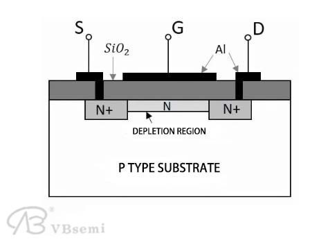
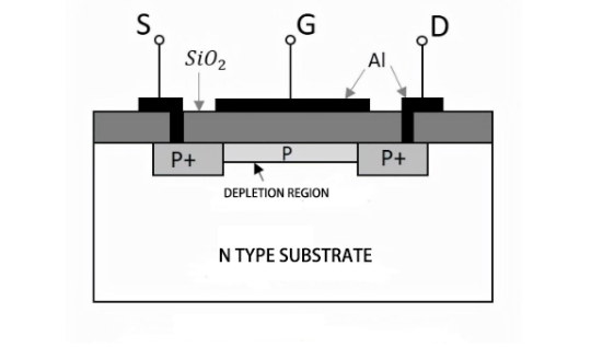
The biggest distinction lies in their substrate (structure). In circuit diagrams, NMOS has a P-type substrate, while PMOS has an N-type substrate. This is the most intuitive method of differentiation.

Forms of NMOS and PMOS switching circuits: NMOS conducts at high level and turns off at low level. PMOS: Conducts at low level and turns off at high level. Summary: Conduction condition is high for N and low for P.
Direction of the arrow in circuit symbols: The arrow pointing towards the gate (G) indicates an N-channel. The arrow pointing away from the gate (G) indicates a P-channel.

On-resistance: NMOS: Has a lower on-resistance, suitable for rapid switching operations. PMOS: Has a higher on-resistance, resulting in slower switching speeds. Both NMOS and PMOS have an on-resistance after conduction, leading to conduction loss. Rds(on) = Vds / (k(Vgs - Vth)^2)

Direction of current: For NMOS, it flows from the drain (D) to the source (S). For PMOS, it flows in the opposite direction, from S to D.

The appearance of NMOS and PMOS can sometimes be distinguished by visual inspection. Typically, the die of an NMOS is darker, appearing gray or black, while the die of a PMOS is lighter, appearing pale yellow or pale blue.
NMOS: Usually has a layer of metal (such as tungsten or copper) covering the oxide film.
PMOS: Usually has a layer of insulating material (such as silicon nitride or alumina) covering the oxide film.

By mastering any one of these points, we can distinguish between NMOS and PMOS.
0 notes
Text
How did NMOS come about? How has it developed?
When we talk about mos, most people are familiar with the term.
The "N" in Nmos comes from the word Negative, indicating that the primary charge carriers involved in conduction are negatively charged electrons in this type of semiconductor.
nmos is a form of mos that uses N-type semiconductor material as the conductive channel.
The Birth of mos:
In 1962, Dawon Kahng and Martin Atalla from Bell Labs in the United States successfully developed the Metal-Oxide-Semiconductor Field-Effect Transistor (mosFET). This invention became a major milestone in the history of semiconductor development, and they are often referred to as the "fathers" of the mosFET.

Early Characteristics and Limitations of Nmos:
Early Nmos technology, with its significant advantages, largely replaced BJT (Bipolar Junction Transistor) in many applications.
1.Higher Switching Speed: Nmos has a higher electron mobility compared to Pmos, meaning electrons move faster in Nmos, and thus Nmos circuits can switch faster.

2.Lower Static Power Consumption: Unlike traditional circuits, Nmos only allows current to flow during switching operations, so it has lower static power consumption in comparison.
Despite its advantages, early Nmos also faced several limitations due to the technology of the time:
1.Higher Dynamic Power Consumption: Early Nmos circuits consumed significant dynamic power during switching, especially when frequently toggling. The charge injection and capacitor discharge during switching led to higher power dissipation.
2.Temperature Sensitivity: Nmos circuits were quite sensitive to temperature variations. As temperature increased, the resistance of Nmos devices rose, leading to a decline in performance and potentially affecting circuit stability.

However, technology continued to evolve, and semiconductor advancements led to innovations in Nmos.
Modern Nmos devices are integrated into billions of transistors in processors and memory chips. Thanks to advanced photolithography techniques, Nmos devices are now mass-produced on a large scale.

In the ongoing pursuit of technological advancements, every turning point brings a revolutionary change, reshaping our understanding of the world.
In the 1980s, Nmos reached another transformative milestone with the introduction of Cmos (Complementary Metal-Oxide-Semiconductor) technology, which became the dominant technology in integrated circuits.

Cmos combines the strengths of both Nmos and Pmos, utilizing complementary working principles to achieve low power consumption, high speed, and high integration.
This innovation was a brilliant response to traditional challenges in semiconductor technology, allowing for better efficiency and greater versatility. Cmos technology has continued to expand its applications and is now the driving force behind the development and innovation of modern electronic products.

From the early days of single Nmos transistors to today's widespread use of Cmos technology, Nmos has undergone decades of development and innovation. Its applications have steadily penetrated our daily lives, often without us even noticing.
In the future, the continued innovation in Nmos will shape our lives and unlock unprecedented possibilities.
0 notes
Text
To understand pmos in mosfets,three key concepts are enough.
1 note
·
View note
Text
Three Key Concepts to Quickly Understand PMOS in MOSFETs
To understand PMOS, we first need to know: what is MOS? MOS stands for Metal-Oxide-Semiconductor Field-Effect Transistor. As the name suggests, M stands for metal, O for oxide, and S for semiconductor. In summary, it is a type of semiconductor device that uses metal and oxide layers.
In electronic circuits, metals are used when conductivity is needed, and insulating materials are used when conductivity is not needed. So, how do we get something that can both conduct and not conduct electricity? The answer is semiconductors.

Today, we are discussing MOS, which is one type of semiconductor. MOS has semiconductor properties that allow it to conduct electricity at times and insulate at others, acting as a switch in the circuit. PMOS is a type of MOS distinguished from NMOS by the channel type.
PMOS Working Principle
(Electronic switch)
Since PMOS functions as a switch, we need to understand how it turns on and off. First, we need to know that PMOS has an n-type substrate and a p-type channel. The direction of the current is from the source to the drain, carried by the flow of holes.
(Low-Level Drive)
PMOS is a low-level drive circuit, meaning that when the gate-source voltage (Vgs) is below a certain value, it will turn on. This is suitable when the source is connected to VCC (high-side drive). On the other hand, when Vgs is greater than or equal to a certain value, PMOS will turn off. In this way, the gate voltage acts like an invisible hand that controls whether PMOS is on or off by controlling the voltage level, thereby forming or cutting off the current in the circuit. Isn't it fascinating?

Advantages of PMOS
As one of the key players in MOSFETs, PMOS has irreplaceable functions and advantages.
1、Low Noise: PMOS has lower noise than NMOS, making it suitable for use in analog circuits.
2、High Threshold Voltage: PMOS typically has a higher threshold voltage, providing strong interference resistance.
3、Low Power Consumption: In a static state, PMOS has low current loss.
Applications of PMOS in Different Industries
(Large electronic demand households)
Thanks to its advantages, PMOS has penetrated various industries, and you can find its presence in many devices you use every day. In terms of market applications, the number one sector is consumer electronics. Devices like smartphones and tablets, which you are likely familiar with, all feature PMOS. PMOS is mainly used in key components such as microprocessors, memory chips, and display driver circuits, helping these devices maintain long battery life.

The second sector is computer networks, including processors, memory, and routers. PMOS plays roles in data storage, logical computation, and signal regulation. Third on the list are network communications, industrial control, automotive electronics, and power equipment. The demand for MOSFETs in these industries is also high, especially in automotive electronics, which now rivals consumer electronics in MOSFET demand.
Future Development of PMOS
The future development of PMOS transistors will focus on improving performance, reducing power consumption, increasing integration, and expanding application areas. New materials, advanced manufacturing processes, 3D integration technologies, and integration with emerging technologies like artificial intelligence and quantum computing will be the main directions for PMOS development.

0 notes
Text
VBE2610N MOSFET In the sweeping robot and the vacuum cleaner:Intelligent control and efficient drive
In order to make the sweeping robot really play a role, intelligent control and efficient driving are very important. In the design and application of the sweeping robot (EV) vacuum cleaner, the selection of the right MOSFET is the key. As one of the core components of the sweeping robot vacuum cleaner, the performance of MOSFET directly affects the charging efficiency, system stability and the long life of the equipment. Our MOSFET product, VBE2610N- -VB-semi, is widely used in this scheme because of its low on resistance and high threshold voltage, high efficiency and high reliability. It provides stable and reliable power support for these components, ensures the efficient operation of the robot in a variety of complex environments, and improves the cleaning effect and intelligence level.
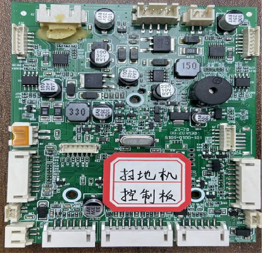
Power management system:
As a kind of intelligent home appliance, the sweeping robot contains a complex circuit system inside, among which the power management module is very important. MOSFET Can be used as the core element of the regulator in the power switch module, VBE2610N high performance and low on resistance characteristics make it very suitable for the sweeping robot and vacuum cleaner power management module, through the accurate control of the current and voltage, to achieve the stable output of the circuit. It can provide efficient electricity conversion and stable current output, thus extending the battery use time and improving the overall energy efficiency of the equipment.
Intelligent control:
In the sweeping robot, intelligent control functions such as path planning, automatic obstacle avoidance, intelligent scheduling and so on all need high-precision circuit control. VBE2610N The high reliability and stability make it a key component of these intelligent control functional circuits, which can ensure that the sweeping robot can achieve efficient cleaning and intelligent operation in a variety of complex environments

Efficient drive:
Sweeping robots are usually equipped with motor drive components such as the main brush and side brush, which require precise current and voltage control to achieve efficient cleaning effect. VBE2610N Has high voltage resistance, can work steadily in high voltage environment, ensure the safety and reliability of electric tools, and reduce the power loss and improve the power density, VBE2610N high current carrying capacity and stable voltage control ability make it the ideal choice in the motor drive circuit, to ensure that the motor under a kinds of load conditions can run operation, provide stable power output.

Applications in other areas
In the wireless communication equipment power amplifier module:
VBE2610N Using trench process manufacturing, with low conduction resistance and high current processing capacity, with high efficiency, high reliability and high current processing capacity, making VBE2610N become one of the indispensable electronic components in wireless communication equipment, help to improve the performance and reliability of the whole system.
In the LED lighting drive
VBE2610N As an MOSFET suitable for high-power applications, it shows significant advantages in LED lighting drivers. It can not only provide accurate power control, through adjusting the conduction state to adjust the LED light intensity, meet the demand of diversified lighting, also because of its low conduction resistance and achieve high efficiency conversion, reduce power loss, its TO252 packaging form easy to integrate and encapsulation, save space, improve the compactness of lighting system and stable stability and extend the service life.

Product Parameter
Product model number: VBE2610N
Polarity: P channel
drain-source voltage (VDS):60V
Grid source voltage (VGS): ± 20V
Threshold voltage (Vth):1.7V
On-on resistance (RDS(on)@VGS=4.5V): 72m Ω
On-on resistance (RDS (on) @ VGS = 10 V): 61mΩ
Maximum drain current:30A
Technology: groove(groove type)
Package: SOT 252
VBE2610N MOSFET—VB-semi has the characteristics of low on resistance and high threshold voltage, high efficiency, high reliability, widely used in sweeping robot and vacuum cleaner, can also be used in voltage regulator, power switch module and other fields. Such as the power amplifier module, LED lighting driver in the wireless communication equipment. Its low threshold voltage and large rated leakage electrode current also make it an ideal choice for home appliance control module, industrial motor controller and other fields. VBE2610N Can improve the performance and competitiveness of its products, to bring users a better use experience and more high-quality, efficient and reliable products.


0 notes
Text
VBI1322 MOSFETs in Automotive Body Control: Enhancing Function Management and User Experience
Body Control System:
The body control system is responsible for managing and controlling the electrical devices inside and outside the vehicle, including features such as headlights, wipers, mirrors, seats, and windows. The efficient and stable operation of this system directly affects driving safety and the level of vehicle intelligence. MOSFETs play a crucial role in body control systems, enhancing the system's functionality management and improving user experience.

1. Precise Power Control
The VBI1322 MOSFET provides precise power control, ensuring stable power delivery to in-vehicle devices, such as seat heaters and window lifts. Its low on-resistance (30mΩ at VGS=2.5V and 22mΩ at VGS=4.5V) improves efficiency and reduces energy loss.
2. Load Switching and Management
The VBI1322 can quickly switch the operational state of various loads, supporting flexible control of functions such as seat heating and window lifting. With a maximum drain current of 6.8A, it meets the power requirements of most automotive electrical devices.

3. Fault Protection Mechanism
In a body control system, electrical devices may suffer damage due to overcurrent, overheating, or other faults. The VBI1322 MOSFET can swiftly disconnect the power supply to protect the circuit from damage.
4. Headlight Control
The VBI1322 MOSFET is suitable for controlling low-power headlights, such as interior lighting or low-power exterior lights. Its stable current control helps prevent current fluctuations from affecting the system, ensuring reliable operation of the headlights and improving driving safety.
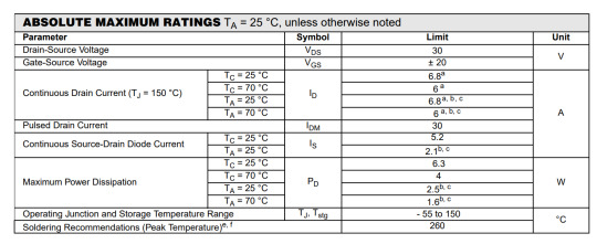
Product Specifications:
Model: VBI1322
Brand: VBsemi
Type: Single N-Channel MOSFET
Rated Drain-Source Voltage (VDS): 30V
Rated Gate-Source Voltage (VGS): 20V
Threshold Voltage (Vth): 1.7V
Drain-Source On-Resistance (Rds(on)) at VGS=2.5V: 30mΩ
Drain-Source On-Resistance (Rds(on)) at VGS=4.5V: 22mΩ
Maximum Drain Current (ID): 6.8A
Technology: Trench (Trench Type)
Package: SOT89

The VBI1322 MOSFET, with its low on-resistance, moderate drain current capacity (6.8A), and low threshold voltage (Vth = 1.7V), is particularly suitable for low and medium-power body control applications, such as seat heaters, window lifts, and interior lighting. It provides precise power control, efficient load switching, and stable current transmission, ensuring efficient operation and system safety in automotive body control systems.
0 notes
Text
Applications of MOSFETs in Vehicle Communication—VBA2412 and VB2355
youtube
2 notes
·
View notes
Text
Applications of VBA2412 and VB2355 MOSFETs in Vehicle Communication Control: Enhancing System Reliability and Data Transmission Security
Vehicle Communication Control The vehicle communication control system is responsible for receiving, processing, and managing various data streams within and outside the vehicle. These include driver identification, real-time vehicle status monitoring, accident information recording and transmission, remote fault diagnosis, and onboard navigation. The efficient and stable operation of vehicle communication control directly impacts vehicle safety and intelligence. In this context, MOSFETs play a crucial role in enhancing system reliability and data transmission security.

Product Specifications

VBA2412:
Operating Voltage (VDS): -40V
Maximum Tolerance Voltage (VGS): 20V
Threshold Voltage (Vth): -2V
On-Resistance at VGS=4.5V: 14mΩ
On-Resistance at VGS=10V: 10mΩ
Maximum Drain Current (ID): 16.1A
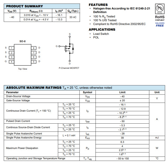

VB2355:
Polarity: Single P-Channel
VDS: -30V
Maximum Tolerance Voltage (VGS): 20V
Threshold Voltage (Vth): -1.7V
On-Resistance at VGS=4.5V: 54mΩ
On-Resistance at VGS=10V: 46mΩ
Maximum Drain Current (ID): -5.6A
Technology: Trench
Package: SOT23-3

Application Scenarios
Signal Amplification and Filtering MOSFETs can amplify weak signals, ensuring clear and interference-resistant sensor data transmission.
VBA2412: With low on-resistance (14mΩ at VGS=4.5V, 10mΩ at VGS=10V), it is suitable for high-current signal amplification, enhancing stability.
VB2355: Its higher on-resistance is ideal for low-power signals, performing well in fine data transmission.
High-Speed Switching Control MOSFETs provide rapid switching performance, ensuring real-time response in high-frequency applications.
VBA2412: Its fast response and 16.1A drain current make it suitable for high-frequency, high-power switching, ensuring data transmission in real-time.
VB2355: Designed for low-power, high-speed signal switching, it’s ideal for signal processing in small modules.
Power Management MOSFETs manage power supply according to module requirements, providing stable current and saving energy.
VBA2412: High current capacity supports power management in high-power modules.
VB2355: Performs well in energy-saving mode for small communication modules.
Overcurrent Protection MOSFETs can detect abnormal currents and quickly cut power to prevent communication module damage.
VBA2412: Suitable for overcurrent protection in high-current conditions.
VB2355: Protects low-power devices, preventing damage to small equipment.
Low Power Control MOSFETs reduce energy consumption in low-power modes, extending system standby time.
VBA2412: Ideal for sustained power supply modules with low-power performance in high-power operations.
VB2355: Extends standby time in small systems during low-power mode.
Advantages and Focus of VBA2412 and VB2355 The VBA2412 is more suitable for high-power, high-frequency applications such as signal amplification, fast switching, and overcurrent protection. The VB2355, on the other hand, excels in low-power, low-noise applications, ideal for signal isolation and low-power control. Together, they complement each other in vehicle communication control applications.
The VBA2412 and VB2355 MOSFETs provide robust support for vehicle communication control in modern intelligent connected vehicles, optimizing data processing and power management. They improve system stability and response speed, ensuring effective power and signal management and protection. These components play a crucial role in enhancing the reliability and energy efficiency of communication modules, laying a foundation for communication control in future smart vehicles.
1 note
·
View note
Text
Application of VBE1638 MOSFET in Automotive Instrument Control Units: Enhancing Power Management and Signal Processing
youtube
0 notes
Text
How to Quickly Identify MOSFETs?
youtube
Some people say they’ve been studying MOSFETs for a long time but still find it hard to grasp. Is it really that difficult?
Today, let's explain MOSFETs in the simplest way possible.
How to Identify the Three Terminals:
We know that MOSFETs have three terminals:

Gate (G): The gate is the easiest to identify.
Source (S): Whether it's a P-channel or an N-channel MOSFET, the intersecting lines indicate the source terminal.
Drain (D): Regardless of the channel type, the side with the single lead is the drain terminal.
These three terminals are used to connect the external circuit.

G (Gate): Controls the MOSFET by changing the voltage level, which directly turns the MOSFET on or off.
D (Drain) and S (Source): These terminals function as the two ends of the switch circuit, one connected to the power supply and the other to ground.
How to Distinguish Between N-channel and P-channel:
It’s quite simple, just look at the symbol:
If the arrow points away from the gate, it's a P-channel MOSFET.

If the arrow points toward the gate, it's an N-channel MOSFET.

Direction of the Parasitic Diode:
If the arrow of the parasitic diode points from the source to the drain, it's an N-channel MOSFET.
If the arrow points from the drain to the source, it's a P-channel MOSFET.


This parasitic diode plays a crucial role in circuit isolation. It helps in over-voltage protection by conducting excess current to the ground, preventing MOSFET damage. It also protects the MOSFET when the source and drain are reversed or when reverse-induced voltage occurs in the circuit.
Once you understand these basic principles, using MOSFETs becomes much simpler.
0 notes
Text
Application of VBE1638 MOSFET in Automotive Instrument Control Unit: Enhancing Power Management and Signal Processing
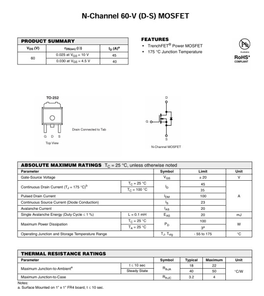
With the continuous advancement of automotive electronics technology, the Instrument Control Unit (ICU) serves as a crucial module in automotive electronic systems, responsible for processing and displaying key vehicle information. To meet the high demands for efficiency and reliability in modern vehicles, the ICU module requires superior performance in power management and switching control. The VBE1638 MOSFET, launched by VBsemi, provides an ideal solution with its excellent electrical characteristics, significantly improving the efficiency of signal processing and power management in ICU modules.

Efficient Power Management The ICU module must achieve stable power management under various load conditions, and the VBE1638, with its 60V drain-source voltage and maximum drain current of 45A, meets the demands of high-power applications. Utilizing advanced trench technology, it reduces on-resistance (with a typical value of only 25mΩ), which minimizes power loss, enhances power management efficiency, reduces heat generation, and extends the lifespan of the device.
Precise Signal Processing Precise signal processing is critical in automotive ICU modules, especially when dealing with complex sensor data. The VBE1638 MOSFET, with its low threshold voltage of 1.7V, enables quick response, ensuring the circuit can switch rapidly and adapt to different working states. Its +20V gate-source voltage (V<sub>GS</sub>) ensures high reliability and stability in various driving environments.
Robust Thermal Performance The automotive environment is highly demanding, requiring ICU modules to operate stably over long periods under high temperatures, vibrations, and current fluctuations. The VBE1638, packaged in a TO252 casing, offers excellent thermal performance, effectively preventing overheating in high-temperature environments, ensuring long-term stable operation, and reducing vehicle system maintenance costs.
Application Advantages The VBE1638 MOSFET is widely used in automotive instrument control unit modules, with optimized power management and power control performance ensuring reliable operation under varying load conditions. Whether in power management systems or complex control scenarios, the VBE1638 delivers stable and efficient performance.
Product Specifications
Model: VBE1638
Package: TO252
Polarity: N-channel
Drain-Source Voltage (VDS): 60V
Gate-Source Voltage (VGS): +20V
Threshold Voltage (Vth): 1.7V
On-Resistance (RDS(on) @VGS=4.5V): 30mΩ
On-Resistance (RDS(on) @VGS=10V): 25mΩ
Maximum Drain Current (ID): 45A
Technology: Trench
Other Applicable Areas
Power Tools: In the power tool sector, such as drills and hammers, MOSFETs provide stable power output. With its high current-handling capacity and low on-resistance, the VBE1638 is an ideal choice for these modules, ensuring high efficiency and stable performance under heavy workloads.
Industrial Automation: The VBE1638 is suitable for industrial automation equipment, including PLC controllers and motor drivers, supporting efficient automation and continuous innovation in smart manufacturing systems.
LED Lighting: In LED lighting applications, the VBE1638 is used in LED driver modules, providing stable and efficient power support, ensuring long life and low energy consumption for LED lamps, streetlights, and landscape lighting products.
As a high-performance MOSFET designed for automotive instrument control unit modules, the VBE1638 excels in power management and signal processing. Whether in complex signal processing scenarios or high-load power management, it helps enhance the overall efficiency and stability of ICU modules. As automotive electronics continue to evolve, the VBE1638 will play a vital role in more automotive applications, contributing to the innovation and upgrading of automotive electronic systems.
#MOSFETs,#Semiconductor,#Electronics,#Technology ,#Automotive,#Power management#On-resistance#Signal processing
0 notes
Text
The Munich Electronics Fair in Shenzhen opens today, with a three-day event showcasing the latest in electronic technology.
youtube
Weibi's booth is located in Hall 1, Booth 1J21. It's a rare opportunity to meet in person! The event will be held at the Shenzhen International Convention and Exhibition Center - Bao'an New Hall from October 14th to 16th. Come join us for an exciting technical discussion on-site!
0 notes
Text
See you tomorrow! 1 day left until the Shenzhen Munich South China Electronics Fair!🥳🎉🎉🎉
0 notes