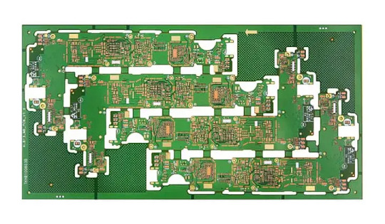
#10-Layer PCB Stack-Up
Explore tagged Tumblr posts
Visit Tumblr Blog
Explore Tumblr blogs with no restrictions, modern design and the best experience.
Last Seen Tumblr Blogs


full-hd-streamingvf-lepeupleloup
LE PEUPLE LOUP Streaming VF HD en Complet en VOSTFR (LE PEUPLE L
1 post


Fun Fact
28.6 is the average number of monthly visits per US mobile user.
Text
Dive into the complexities of 10-layer PCB stack-up with this comprehensive guide. Viasion outlines key design principles, layer configurations, and considerations to ensure optimal performance, signal integrity, and reliability in multilayer board designs.
0 notes
Text
Looking Back
Today, 26 March 2025, is the tenth anniversary of the first time I put power to a Z80 microprocessor in a breadboard and watched it blink some LEDs.

Within a few weeks that Z80 would be completely surrounded by other chips and hundreds of wires to form my first functioning homebrew computer.

Another week and I was already removing a 68000 from a (presumed) dead motherboard, with grand ideas of moving up to the 16-bit era (but absolutely no understanding of what that would entail)

It would be another two years before the first time I put that 68000 in a breadboard and successfully used it to blink an LED.

By the time another year had rolled around that 68000 was living on a soldered breadboard and for the first time on one of my projects, it was running real software — EhBASIC.

Always looking to more challenging projects, while I was building with a 68000, I was already reading through the manual for the 68030 trying to understand how to build with a proper 32-bit microprocessor. Just one more year and I had that 68030 on a wire wrap board, blinking an LED.

The next year I was doing the most ridiculous thing I could think of — free-running a Pentium CPU on a wire wrap breadboard to blink an LED. Because I could.

By the end of the next year that 68030 had moved from its wire wrap board onto a proper printed circuit board — my first ever 4-layer PCB.

The next year saw the towering expansion of the 68030 build, adding new peripherals and functionality.

Another year and I had an all-new 68030 build on a Micro-ATX form-factor motherboard developed in just a couple months ahead of VCF Southwest 2023.

The next year I focused on developing software for my existing 68030 board stack, rather than building something new from scratch. I succeeded in developing a minimal multi-user kernel to run four instances of BASIC simultaneously.
All along in between working on these projects I have done component-level repairs on various computers, developed expansion cards for the Mac SE, built PCs both new and old, burned out hard, developed some smaller homebrew computers, had a lot of false starts, failed projects, and abandoned projects, and completed some massive projects in my day job.
Looking back at everything I've worked on over these past 10 years I am absolutely amazed at how far I have come and what I have been able to accomplish. Much of it I still don't understand how I managed to actually pull it off, and I'm not entirely sure I could duplicate my successes.
Here's to the next ten years
#homebrew computing#homebrew computer#retro computing#retrocomputing#ten years#learning new things#zilog z80#motorola 68k
81 notes
·
View notes
Text
Rigid-Flex PCB Design Guidelines: Ensuring Reliability and Manufacturability
Designing a Rigid-Flex PCB requires more than just combining rigid and flexible sections into one board. It involves careful planning of layout, layer structure, materials, and mechanical constraints to ensure the final product is reliable, manufacturable, and cost-effective.
Below are key guidelines every engineer should follow when designing Rigid-Flex PCBs.
1. Define Rigid and Flex Zones Early
Clearly identify the rigid and flex areas during the initial layout phase. Flex regions should only exist where necessary — overdesigning with too much flex area increases cost and complexity.
Each zone should be planned based on:
Mechanical movement (bending/folding)
Component placement needs
Connector and housing locations
Avoid placing unnecessary flex areas just for routing convenience unless absolutely needed.
2. Maintain Symmetrical Layer Stack-Up
An unbalanced stack-up can lead to warping, twisting, or delamination during lamination or reflow.
Keep the number and thickness of layers symmetrical around the centerline of the rigid section.
Use dummy traces or copper balancing layers to achieve mechanical balance if needed.
Plan separate stack-ups for rigid and flex areas, but ensure transition is smooth.
3. Protect the Flex Area
The flexible section is vulnerable to cracking and wear if not designed carefully.
Never place vias, pads, or components in the flex zone.
Maintain generous spacing between traces in the flex area to reduce mechanical stress.
Avoid 90° corners and sharp transitions — use smooth curves or teardrops for trace routing.
Use coverlay (instead of solder mask) to protect the flex area from mechanical damage.
4. Follow Proper Bending Design Rules
The flex section must withstand multiple bends over its lifetime. Improper bending design can cause trace cracking, delamination, or copper fatigue.
Minimum bend radius should be 6 to 10 times the flex thickness for dynamic bends.
For static (one-time) bends, 3 to 6 times the thickness may be acceptable.
Use curved traces in the bend area to avoid concentration of stress.
Keep traces perpendicular to the bend axis wherever possible.
5. Stiffener Usage
Stiffeners are added in flex areas to provide mechanical support for connector pads or component locations.
Use FR4, polyimide, or stainless steel stiffeners depending on mechanical requirements.
Clearly define stiffener thickness and position in the mechanical drawings.
Do not overlap stiffeners with bend areas unless absolutely required.
6. Routing and Trace Layout
Trace layout impacts both electrical and mechanical performance.
In the flex region, use wide, evenly spaced traces to reduce stress.
Avoid overlapping traces on top and bottom layers in bend areas.
Do not route traces over the transition zone between rigid and flex — leave a clearance buffer.
Maintain consistent impedance and routing lengths for high-speed signals.
7. DFM Considerations
Design for Manufacturability (DFM) is critical for Rigid-Flex PCBs due to the multiple lamination cycles and tighter tolerances.
Ensure design files clearly mark flex/rigid regions and bending direction.
Avoid complex via structures (like stacked or blind/buried vias) near flex zones.
Confirm with the PCB manufacturer about acceptable layer counts, material systems, and bend performance.
Work closely with your fabricator early in the design process to avoid costly revisions.
8. Assembly Planning
Plan your PCB assembly process around the flex structure.
Use support fixtures or carrier panels during SMT to keep the board flat.
Make sure flex areas are protected during handling and soldering.
Define handling instructions clearly if the flex zone should not be bent before final assembly.
Final Thoughts
Rigid-Flex PCBs offer unmatched versatility for compact, high-performance designs — but only when designed correctly. By following key guidelines for stack-up, routing, bending, and assembly, designers can ensure their boards are reliable, manufacturable, and optimized for long-term success.
Collaborate closely with your PCB manufacturer and assembly house throughout the design process to turn your concept into a robust, production-ready product.
0 notes
Text
Structural Innovation and Easy Installation Technologies in Power Socket Design

As smart homes, office automation, and industrial digitalization rapidly advance, the demand for user-friendly, efficient, and safe power sockets continues to grow. Traditional socket designs are no longer sufficient for fast-paced environments that require high reliability, ease of installation, and space optimization. This has driven innovation in both internal structure and external mounting mechanisms of modern power sockets.
This article explores key advancements in structural design and installation technologies of power sockets, focusing on terminal innovations, mounting bracket designs, and strategies to increase module density without increasing volume. We will also discuss real-world examples and applicable technologies for B2B manufacturers and system integrators.
1. Integrated vs. Modular Terminal Design: Which is More Efficient?
The terminal structure of a power socket directly determines wiring efficiency and stability. The two mainstream types are:
A. Integrated Terminal Block (One-Piece)
All terminals are integrated into a single housing.
Benefits: Shorter installation time. Reduced loose contacts. Lower resistance due to shorter conductive paths.
Limitations: Less flexible for modular replacement. May increase overall production complexity.
B. Modular Terminal Block (Multi-Part)
Each terminal is separately assembled or replaceable.
Benefits: Ideal for custom configurations. Easier to repair and replace.
Limitations: Longer assembly time. Risk of performance inconsistency.
2. Push-in Spring Connection Technology: Fast, Safe, Tool-Free Wiring
Compared to screw terminals, push-in spring terminals provide:
Quick installation: Simply push the stripped wire into the terminal.
Strong contact: Stainless steel or beryllium copper springs maintain pressure for years.
No need for torque tools: Reduces operator training and tool investment.
🔧 Case Example: A European power socket brand uses a push-in spring design that allows a full 5-gang module to be wired in under 30 seconds — 60% faster than screw terminals.
3. Quick-Mount Bracket Designs: Screw-Free, Time-Saving, and Reliable
In large-scale installations (e.g., hotels, office buildings), fast mounting systems dramatically reduce labor costs and error rates.
Key Innovations:
A. Snap-In Mounting Frame
Socket modules are inserted directly into wall plates with audible clicks.
Uses elastic clips or sliding locks for firm placement.
Ideal for drywall and modular building systems.
B. Screwless Embedded Mounting
Eliminates screw holes by using slide-in rail structures.
Allows easy front-facing maintenance or upgrades.
Common in premium wall systems and panel furniture.
C. Magnetic or Cam-Lock Fastening
Applies in high-end modular offices.
Enables tool-free repositioning.
🔧 Case Example: A Chinese manufacturer developed a double-locking quick-install bracket that passed 500N pull force tests, suitable for vibration-prone environments like rail stations.
4. Increasing Module Density Without Expanding Volume
Modern installations demand multi-functionality in limited space. Techniques include:
A. Vertical Layering of Internal PCB
Using 3D layout: control, relay, and detection circuits are stacked.
Reduces horizontal footprint while maintaining thermal separation.
B. Multi-Function Integration
Combining USB chargers, smart sensors, and energy monitors in one unit.
Example: A 55x55mm wall socket includes 2 USB-A ports, 1 USB-C PD port, and Wi-Fi controller.
C. High-Density Terminal Design
Dual-row spring contacts with insulation barriers allow up to 10 terminals in standard footprint.
Ensures safety spacing while maintaining compact size.
5. Material Innovation: Making Structural Compactness Possible
A. High-Performance Plastics:
Use of PA66, PC+ABS, and flame-retardant PBT with thin-wall molding tech.
Improves space efficiency without sacrificing insulation performance.
B. Conductive Material Optimization:
Use of laminated copper busbars.
Electroplated or stamped silver contact surfaces to reduce thickness.
6. Installation Aids and Engineering Enhancements
A. Color-coded Wiring Guides:
Reduces wiring errors during bulk installations.
Accelerates compliance with local electrical codes.
B. Pre-assembled Harnesses:
For standard socket layouts, pre-assembled wire bundles reduce on-site labor.
C. Tool-Assisted Plug-In Systems:
Modular rail sockets with plug-in interfaces (e.g., DIN-rail smart outlets) improve interchangeability.
7. Structural Testing and Validation

8. Conclusion: Towards Smarter, Faster, and Denser Power Socket Design
Power socket structure and installation are no longer just mechanical tasks—they are core parts of user experience, energy efficiency, and engineering cost control. Through structural innovation like push-in terminals, quick-install brackets, and functional integration in compact modules, manufacturers can deliver plug-and-play, space-saving, and intelligent power socket solutions.
Whether you're a B2B buyer, an engineering contractor, or a systems integrator, adopting these next-generation socket designs will result in lower maintenance costs, faster deployment, and greater end-user satisfaction.
en.dghongju.com
0 notes
Text
How to Design Efficient and Reliable Rigid-Flex Circuit Boards?
Rigid-Flex Circuit Boards combine the best highlights of rigid and flexible PCBs into a single bound together structure, advertising creators effective focal points for complex and space-constrained applications. These hybrid Boards are composed of rigid layers that give mechanical soundness and flexible areas that permit energetic development or collapsing. To accomplish both proficiency and unwavering quality in rigid-flex circuit board plan, engineers must take after a set of best hones that consider mechanical, electrical, and fabricating aspects.
Understand the Application Requirements
Before starting the format, it's basic to get it the particular needs of the application. Rigid Flex Circuit Boards are frequently utilized in aviation, military, therapeutic gadgets, and progressed shopper hardware — all situations that request tall unwavering quality. Architects must consider space limitations, mechanical stretch, electrical execution, and natural introduction to guarantee that the board meets execution and solidness expectations.
Use Legitimate Layer Stack-Up Planning
A well-structured layer stack-up is key to accomplishing flag keenness and mechanical quality. In rigid-flex circuit Boards, the move between the unbending and flexible areas must be smooth and free of push concentration. Legitimate stack-up arranging incorporates deciding the number of layers, copper weight, dielectric materials, and the twist span of flexible locales. Dodging as well numerous layers in the flex range makes a difference avoid delamination and splitting over time.

Maintain Controlled Twist Areas
One of the most common focuses of disappointment in rigid-flex plans is the twist zone. To guarantee long-term unwavering quality, the twist span ought to be at slightest 10 times the thickness of the flex fabric. Twists ought to never happen at the interface between unbending and flexible segments. Moreover, dodge putting vias, cushions, or sharp points in the twist region to decrease mechanical stretch. Utilize bended follows and stunned vias to upgrade adaptability and decrease the hazard of cracking.
Optimize Follow Routing
Efficient directing is fundamental for flag keenness and control dissemination. In rigid-flex circuit Boards, follows ought to be directed opposite to the twist pivot in flexible areas. Parallel follows in a twist range are more likely to break over time. Keep up steady follow widths and dividing, and maintain a strategic distance from 90-degree points in steering, as they can cause flag reflections and push focuses. Controlled impedance plan is moreover imperative for high-speed flag transmission.
Design for Manufacturability (DFM)
Working closely with your PCB manufacturer amid the plan stage can avoid expensive modifications. Utilize standard materials and take after industry rules like IPC-2223 for rigid-flex board plan. Indicate clear mechanical diagrams, resistances, and stack-up subtle elements in the manufacture drawings. Too, incorporate fiducials and test focuses to help in get together and review processes.
Include Intensive Testing and Validation
To guarantee the long-term unwavering quality of rigid-flex circuit Boards, intensive testing is basic. This may incorporate warm cycling, vibration tests, and electrical testing beneath stack. Early approval makes a difference capture plan blemishes and guarantees the board can perform in real-world conditions.
Conclusion
Designing effective and dependable rigid-flex circuit Boards requires a mindful approach that equalizations electrical execution with mechanical judgment. By carefully arranging the layer stack-up, overseeing twist ranges, optimizing follow steering, and centring on manufacturability, engineers can make progressed gadgets that are both compact and tough. With legitimate testing and adherence to plan benchmarks, rigid-flex Boards gotten to be a trusted arrangement for today’s most requesting electronic applications.
0 notes
Text
PCB Manufacturing: A Comprehensive Guide to Printed Circuit Board Production

Introduction to PCB Manufacturing
PCB manufacturing is the process of creating printed circuit boards, which are essential components in nearly all modern electronic devices. From smartphones to industrial machinery, PCBs provide the foundation for electrical connections and component mounting. This guide explores the PCB manufacturing process, materials, technologies, and applications.
The PCB Manufacturing Process
1. Design and Schematic Creation
Before production begins, engineers design the PCB using specialized software like Altium Designer, KiCad, or Eagle. The design includes:
Schematic diagrams (circuit connections)
Component placement
Trace routing (copper pathways)
Layer stack-up (for multi-layer PCBs)
Once the design is finalized, a Gerber file (standard PCB manufacturing file) is generated for fabrication.
2. Material Selection
The base material of a PCB is typically FR-4, a flame-resistant fiberglass epoxy laminate. Other materials include:
Flexible PCBs: Made from polyimide for bendable circuits.
High-frequency PCBs: Use Rogers material for RF applications.
Metal-core PCBs: Aluminum or copper for heat dissipation.
3. Printing the Circuit Pattern
The PCB design is transferred onto the board using one of these methods:
Photolithography: A UV-sensitive photoresist is applied, exposed to UV light, and developed to create the circuit pattern.
Direct Imaging: A laser directly etches the pattern onto the PCB.
4. Etching the Copper Layers
After the circuit pattern is printed, the unwanted copper is removed through chemical etching. The remaining copper forms the conductive traces.
5. Drilling Holes for Components
Precision CNC machines drill holes for through-hole components and vias (connections between layers).
6. Plating and Copper Deposition
The drilled holes are electroplated with copper to ensure conductivity between layers.
7. Solder Mask Application
A solder mask (usually green) is applied to protect the copper traces and prevent short circuits. Openings are left for soldering components.
8. Silkscreen Printing
Text, logos, and component labels are printed on the PCB using silkscreen ink for easy assembly and identification.
9. Surface Finish Application
A surface finish is applied to protect exposed copper and improve solderability. Common finishes include:
HASL (Hot Air Solder Leveling)
ENIG (Electroless Nickel Immersion Gold)
OSP (Organic Solderability Preservative)
10. Electrical Testing and Quality Control
Each PCB undergoes automated optical inspection (AOI) and electrical testing to ensure functionality. Defective boards are rejected.
Types of PCBs in Manufacturing
1. Single-Layer PCBs
Simplest and most cost-effective.
Used in basic electronics like calculators.
2. Double-Layer PCBs
Conductors on both sides.
Common in consumer electronics.
3. Multi-Layer PCBs
4+ layers for complex circuits (e.g., motherboards).
Requires precise PCB manufacturing techniques.
4. Flexible PCBs
Used in wearables and medical devices.
Made from bendable materials.
5. Rigid-Flex PCBs
Combines rigid and flexible sections.
Ideal for aerospace and military applications.
Advanced PCB Manufacturing Technologies
1. High-Density Interconnect (HDI) PCBs
Features microvias and finer traces.
Used in smartphones and compact devices.
2. Embedded Components
Passive components (resistors, capacitors) are embedded within the PCB.
Reduces size and improves performance.
3. 3D Printed Electronics
Emerging technology for rapid prototyping.
Combines additive manufacturing with conductive inks.
Applications of PCB Manufacturing
PCBs are used in nearly every industry, including:
Consumer Electronics (Smartphones, Laptops)
Automotive (ECUs, Infotainment Systems)
Medical Devices (Pacemakers, Imaging Systems)
Aerospace & Defense (Avionics, Radar Systems)
Industrial Automation (Robotics, Control Systems)
Challenges in PCB Manufacturing
Miniaturization: Shrinking component sizes demand precision.
High-Speed Signal Integrity: Ensuring minimal interference.
Thermal Management: Preventing overheating in dense circuits.
Environmental Regulations: Compliance with RoHS and REACH.
Future Trends in PCB Manufacturing
AI-Driven Design Optimization
Sustainable Materials (Biodegradable PCBs)
5G and IoT Integration (Higher frequency PCBs)
Automated Smart Factories (Industry 4.0)
Conclusion
PCB manufacturing is a complex yet vital process that powers modern electronics. From design to testing, each step requires precision and expertise. As technology advances, printed circuit boards will continue to evolve, enabling smaller, faster, and more efficient devices.
Whether you're an engineer, hobbyist, or industry professional, understanding PCB manufacturing helps in designing better electronic products for the future.
1 note
·
View note
Text

10 layers HDI PCB, manufacturer from China - Hitech Circuits
Base material: FR4, TG170
Surface treatment: ENIG
Board thickness: 1.0mm
Copper thickness: 0.5oz
Minimum line width: 0.1mm
Minimum line spacing: 0.1mm
Laser drilling + blind and buried drilling Impedance control
Board stack up: 1+8+1
Impedance control
Email Cynthia<[email protected]> if you are looking for remarkable HDI printed circuit board.
0 notes
Text
Advancements in Rocket-PCB's 10 Layer ELIC Multilayer PCB Fabrication
Rocket-PCB has revolutionized the PCB industry with its cutting-edge technology, offering high precision any layer HDI multilayer PCB fabrication. Among its impressive array of products is the 10 layer ELIC printed circuit board, crafted with precision and expertise to meet the diverse needs of its users. This article aims to delve into the technical aspects of this remarkable PCB, exploring its materials, design, and manufacturing techniques.
Material and Board Thickness
The 10 layer ELIC PCB from Rocket-PCB is constructed using FR4, a popular substrate material known for its excellent mechanical and thermal properties. FR4 is widely favored in the PCB industry due to its high durability and cost-effectiveness. The board thickness is set at 1.6mm, striking the right balance between stability and space-saving design, making it suitable for various applications, including consumer electronics, industrial equipment, and automotive systems.
Surface Treatment: Immersion Gold
To ensure reliable performance and enhance the PCB’s solderability, Rocket-PCB employs an immersion gold surface treatment. This process involves immersing the PCB in a solution containing gold particles, which form a thin, protective gold layer on the exposed copper traces and pads. The immersion gold surface finish provides excellent electrical conductivity, while also preventing oxidation and ensuring a smooth surface for soldering components.
Stack Up: N+N Configuration
Rocket-PCB utilizes a stack up configuration of N+N for their 10 layer ELIC PCB. The N+N stack up refers to the use of multiple cores and prepreg layers in a symmetrical arrangement to facilitate impedance control and signal integrity. This design allows for the creation of highly complex circuits with improved electrical performance and minimal crosstalk between adjacent signal layers.
Track/Width and Laser Vias
The 10 layer ELIC PCB boasts impressive track/width dimensions of 3/3mil, demonstrating Rocket-PCB’s commitment to providing high precision solutions. The narrow track and spacing enable efficient routing of signals and ensure that the PCB can handle high-frequency signals without signal degradation.
Moreover, the PCB incorporates advanced technology, including laser vias. These vias are created using laser ablation techniques, allowing for smaller via diameters and higher density interconnects. Laser vias are particularly advantageous in high-density designs, where space is limited, and precise signal paths are essential for optimal circuit performance.
Blind and Buried Vias
Rocket-PCB’s 10 layer ELIC PCB fabrication supports blind and buried vias. Blind vias connect an outer layer to one or more inner layers, while buried vias connect two or more inner layers without extending to the outer surfaces. By utilizing blind and buried vias, the PCB achieves higher circuit density, reducing the number of layers required and making it a cost-effective and space-saving solution.
Rocket-PCB’s 10 layer ELIC printed circuit board represents a pinnacle of high precision any layer HDI multilayer PCB fabrication. With its FR4 material, immersion gold surface treatment, N+N stack up configuration, laser vias, and support for blind and buried vias, this PCB exemplifies the cutting-edge technology offered by Rocket-PCB.
Electronics designers and manufacturers can leverage the capabilities of this advanced PCB to meet the demands of modern electronic devices with complex circuitry and high-frequency requirements. Rocket-PCB continues to lead the industry in providing innovative solutions, empowering businesses to create reliable and efficient electronic products for a wide range of applications.
0 notes
Text
Design of High Frequency PCB
You are here because you want to learn about high frequency PCB design. This guide explains in detail different factors having an influence on high frequency PCB. Furthermore, we will discuss different challenges to this type of PCB and solution as well. In short, this comprehensive guide expresses everything you need to know regarding high-frequency PCB design.
High frequency PCB is a type of PCB that have wide usage in different applications such as microwave. So let’s dive in and try to explore different incredible aspects of this technology.
High Frequency PCB
Most of you are familiar with the word PCB. If you are not, it is basically an acronym of the Printed Circuit Board. So PCB uses conductive tracks and paths to connect different components on the circuit board electronically. Copper is the main substance of PCB that provides a conductive path on the board.
In addition to this, signal communication plays a key role in different electronic projects. For example, it is crucial in those projects where Wi-Fi and satellite systems involve. So when there is a need for signal communication between two or more objects, high frequency boards come in usage.
So high frequency PCB is a type of circuit board used for signal transmission. For example, companies use it in the microwave, mobile, radiofrequency and high-speed design applications.
Factors that influence a high frequency PCB Design
There are some important factors that have a high impact on high frequency PCB design. So these boards come with high frequency laminates, that are difficult to fabricate. It is because they need to maintain the thermal heat transfer of different applications.
Circuit boards use special materials to attain a high frequency. So characteristics of the high frequency board affect the overall performance of the signal. Furthermore, a slight change in the ER value of the materials can have an impact on the impedance of the board.
Besides above all, dielectric materials also influence a high frequency PCB design. Most of the manufacturers prefer rogers dielectric material. This material is less expensive and it has low DK and DF value as well. Furthermore, it appears to be suitable for prototyping applications and fabrication. In addition, it also reduces signal loss as well.
On the other hand, some manufacturers go with Teflon. Manufacturers use it in high frequency board manufacturing. Moreover, it basically comes with 5 GHz frequency. Moreover, FR4 is another popular material used for RF applications. The applications require 1 GHz to 10 GHz frequency use FR4. However, FR4 based products have their own limitations and drawback.
So in terms of DF, DK and water absorption factor, Teflon is the finest option. However, it is more expensive than FR4. If your project requires more than 10 GHz frequency, Teflon is the best choice.

General specification of high frequency PCB
To achieve high frequency for your needs, you can use different special materials. Furthermore, any change in the Er value of different materials can have a significant impact on the impedance of the board. You can find PCBs with different frequencies. So the typical range of frequency from 500 MHz to 2 GHz.
However, let’s discuss some generic specification of high frequency PCB:
Material: RO4003C, Ro3003, RT5880 and Ro3010
Board Size: Min 6mm x 6 mm or max 457 mm x 610 mm
PP: Rogers 4450F, Domestic-25FR, Domestic-6700
Board Thickness: 4 mm to 5.0 mm
Copper Weight: 5oz to 2.0oz
Solder Mask Sides: As per the file
Solder Mask Color: Green, Blue, Red, White, and Yellow
Min Tracking or Spacing: 3mil/ 3mil
Silkscreen Sides: As per the file
Silkscreen Color: Black, White, and Yellow
Surface Finish: Electroless nickel/ immersion gold, immersion silver, immersion tin –RoHS
Impedance Tolerance: Plus or Minus 10%
Min Drilling Hole Diameter: 6mil
Min Annular Ring: 4 mil
If you want to purchase the best quality high frequency PCB, MOKO Technology is the best option. You can customize these circuit boards according to your needs. For a consultation, you can contact the professional team of MOKO Technology.
How to identify the best high frequency PCB?
It is not a big deal to identify the high frequency PCB. Look at the general specification and the material used to construct PCBs. So you can identify the high frequency PCB. Otherwise, if you are not familiar, you can consult any trustworthy company such as MOKO Technology.
Different useful tips of high frequency PCB design and manufacture
High frequency circuits have a higher layout density and higher integration. So it is crucial to know how to design and manufacture more reasonable and more scientific circuit boards. Let’s have a look some of the most useful tips:
It is better to have the less alternative leads of the pins between different layers of high frequency circuits,
There should be a shorter lead between the pins.
It is important to have less bend between the pins of high frequency electronic devices.
Try to avoid loops while wiring.
Make sure to have good signal impedance matching.
Furthermore, you should increase the high frequency decoupling capacity of the power pins of an integrated circuit block.
The challenge of high frequency PCB design and how to encounter it
During the manufacturing process, you can face different challenges. Below is a brief overview of some common challenges:
1. Scaling
Most circuit board fabricators are familiar with the concept of artwork scaling. As internal layers lose some mass during the lamination process while building FR4 multilayers PCBs. So it is important to scale-up circuitry by known percentage in anticipation of this loss. So the layers return to their as-designed dimensions after the completion of the lamination cycle.
Moreover, laminate materials behave somewhat differently because of being softer than FR4. However, the idea is almost similar to figure out what the material is likely to do. As it goes through the process. It means you should establish separate scale factors for each type. Furthermore, you should create a separate scale for each thickness within a single type even.
Otherwise, registration from layer to layer or drill to pad can be compromised. The fabricator should use the baseline scaling recommendation of the laminate manufacturer with an in-house statistical process. So it will be consistent over time within the special manufacturing environment.
2. Surface Preparation
Multilayer surface preparation is complex for getting a secure bond between layers. So it is specifically true for Teflon types. Therefore, the soft material can be deformed if the preparation is very aggressive. So significant deformation can lead to poor registration. In addition to this, if the deformation is quite obvious, PCB may end up as a non-functional scrap.
Deburring can actually polish the substrate. This can affect adhesion in multilayers. It is because some materials contain pure Teflon. So this product is renowned for its non-stick nature. To replace this material can be costly and result in long delays as well. The only way to avoid such an outcome is to carefully perform this step. So make sure to perform this step correctly.
3. Hole Preparation
Before plating through with copper, you must remove surface irregularities. You should further remove debris and epoxy smear. As a result, the plating will adhere to the hole walls. RF materials such as ceramic or PTFE/ Teflon need different ways for hole preparation.
In this process, try to adjust different drill machine parameters to prevent the substrate from smearing in the first place. During the hole treatment after drilling, the plasma cycle uses various gases from normal boards. If you fail to prepare the holes before plating, interconnection will be poor. That will fail over time. So it is important to form clean holes for long-term reliability.
4. Thermal Expansion Rates
CTE is another crucial factor for long-term reliability. CTE stands for the coefficient of thermal expansion. Manufacturers use it to measure the amount of expansion of different materials. Expansion can go in any of the three axes under thermal stress. If the CTE is lower, the less likely the plated holes will fail from repeated flexing of the copper.
Furthermore, CTE can be complex if you combine high frequency materials with FR4 in hybrid multilayer PCB constructions. It is because the CTE of one material must match with the other materials. Otherwise, different layers will expand at different rates that can be problematic.
In addition to layers, the same is true for vias as well. So material used for plugging vias should match the other materials as well in the stack. So before manufacturing high frequency PCB design, you should consider this important factor.
5. Machining
There are some RF materials that behave very similar to the FR4 laminates while machining. So it is very important to understand some basic differences. For instance, ceramic-impregnated types can be very hard while drilling through on drill bits. So it is very important to reduce maximum hit counts. Moreover, you should customize spindle infeed and RPM settings.
Fibers can also remain inside hole walls. So these can be very difficult to remove. So try to adjust drilling parameters so that fiber occurrence should be minimized.
0 notes
Text
Sharing a Computer with More Friends
A few months ago I built an I/O expansion board for my homebrew 68030 project with a 4-port serial card to go with it, and got BASIC running for four simultaneous users. It worked, but not as well as I had hoped. I wanted to be able to run two of those serial cards to support 8 total users, but it had proven unstable enough that with just the one card I had to slow down the whole system to 8MHz.
So I designed a new serial card.

I had previously been running this computer without any issues at 32MHz with a mezzanine card with FPU & IDE as well as a video card. The main board by itself can clear 56MHz. Having to go all the way down to 8MHz just didn't sit well with me. I want this machine to run as fast as possible for its 8 users.
I put extra time into reviewing worst-case timing for all components and graphing out how signals would propagate. The 16C554 quad UARTs I'm designing around are modern parts that can handle pretty fast bus speeds themselves — easily up to 50MHz with no wait states on the 68030 bus — assuming all the glue logic can get out of the way fast enough.
Signal propagation delays add up quickly.
My first draft schematic used discrete 74-series logic for chip selection, signal decoding, timing, etc. At slower bus speeds this wouldn't have been a problem. But I want this thing to run as fast as possible. By the time critical signals had made it through all those logic gates, I was looking at already being well into one wait state by the time the UART would see a 50MHz bus cycle begin.
I needed something faster. I was also running low on space on the board for all the components I needed. The obvious answer was programmable logic. I settled on the ATF22V10 as a good compromise of speed, size, availability, and programmability. It's available in DIP with gate delays down to 7ns. Where discrete gates were necessary, I selected the fastest parts I could. The final design I came up with showed a worst case timing that would only need one wait state at 50MHz and none for anything slower.
It ended up being a tight fit, but I was able to make it work on a 4-layer board within the same footprint of my main board, putting some components on the back side. (It may look like a bunch of empty space, but there's actually a lot going on running full RS232 with handshaking for 8 ports).
New problem. I had blown my budget for the project. As much as I love those stacked DE9 connectors, they're expensive. And there's no getting around the $10 pricetag for each of those quad UARTs. Even using parts on-hand where possible, I was looking at a hefty Mouser order.
[jbevren] suggested using ganged RJ45 connectors with the Cisco pinout instead of stacked DE9, to save space & cut costs. [Chartreuse] suggested buffering the TTL serial TX/RX signals to drive the LEDs that are frequently included on PCB-mount RJ45 connectors. Both great ideas. I was able to cut 20% off my parts order and add some nice diagnostic lights to the design.
Two weeks later, I received five new PCBs straight from China. I of course wasted no time setting into starting to assemble one.
I really set myself up for a challenge on this one. I learned to solder some 25 years ago and have done countless projects in that time. But I think this might be the most compact, most heavily populated, most surface mount board I've ever assembled myself. (There are 56 size 0805 (that's 2x1.2mm) capacitors alone!)


After a few hours soldering, I had enough assembled to test the first serial port. If the first port worked then the other three on that chip should work too, and there's a great chance the other chip would work as well.

And it did work! After some poking around with the oscilloscope to make sure nothing was amiss, I started up the computer and it ran just fine at 8MHz.
And at 16MHz.
And at 25MHz.
And at 32MHz.
And at 40MHz.
And almost at 50MHz!
Remember what I said about my timing graphs showing one wait state for 50MHz? The computer actually booted up and ran just fine at 50MHz. The problem was when I tried typing in a BASIC program certain letters were getting switched around, and try as I might, BASIC just refused to 'RQN' my program. It was pretty consistently losing bit 3, likely from that signal having to travel just a tiny bit farther than the others. A problem that will probably be resolved with an extra wait state.
Good enough for a first test! A few hours more and I finished assembling the card.

I did have some problems with cleaning up flux off the board, and I had to touch up a few weak solder joints, but so far everything seems to be working. I've updated my little multi-user kernel to run all 8 users from this new card and it's running stable at 40MHz.
I need to update my logic on the 22V10 to fix a bug in the wait state generator. I would love to see this thing actually running at 50MHz — a 25% overclock for the 40MHz CPU I am currently running. I also want to expand my little kernel program to add some new features like the ability to configure the console serial ports and maybe even load programs from disk.
I hope to bring this machine with a collection of terminals and modems this June to VCF Southwest 2025 for an interactive exhibit that can be dialed into from other exhibits at the show.
#wrap030#multi-user BASIC#EhBASIC#homebrew computer#motorola 68030#68030#mc68030#motorola 68k#vcfsw#vcfsw2025#Retrocomputing#rtc#retrotech crew
31 notes
·
View notes
Text
flexible pcb manufacturing process
flexible pcb manufacturing process

flexible pcb Whenever ordering flex circuit planks online, quick turn order delivery timelines can get setbacks if the information fixed is either imperfect or if your design provides technical concerns. Technical troubles can be relevant to possibly manufacturability or the finish use of the areas. These concerns then frequently require numerous communications for you to resolve and in many worst-case scenarios, extensive layout revision. Any of all these issues will probably of program delay the delivery regarding the finished parts. A prosperous flexible PCB often depends upon two things: the manufacturability of your respective design, and your personal relationship (e. g., amount of collaboration) with your dealer. Say you�ve decided that flex is the suitable fit for your program. By now, you have a bevy of supplemental alternatives in front of anyone. Will you choose a single-sided (with or without a stiffener) or multilayer flex PCB, or could a rigid-flex PCB job in this situation? Can easily your current PCB supplier produce a table that also meets all of these requirements? flexible pcb manufacturer Giving an answer to these concerns and keeping away from costly mistakes and interruptions holdups hindrances impediments is much much easier when you sit down along with your dealer and contrast the options available for your requirements. Relatively simple designs these as single-layer flex tend to be the most affordable, nevertheless cost isn�t anything. Help to make sure the flex PCB you choose is the particular best technical in shape with regard to your use case. Dependent on software, a bigger manufacturing cost may lower on overall expense in the long run. Fork out close attention to often the often the complexity of the actual flex PCB application seeing that well as the abilities and also recommendations of your own supplier. On this page we will probably detail some of typically the more prevalent flex circuit technical concerns we often notice that delay easy convert orders to help a person prevent delays and full assembly and also delivery involving your product as soon as possible. a single. Flex PCB Board simple specification. A part variety (including revision number) to your design to ease monitoring Aboard thickness (. including bend part thickness as well as each stiffener area�s thickness). Type of aboard materials (Polyimide adhesiveless bottom substance or Polyimide adhesive bottom part material, etc). Polyimide inspissated base material is usually typical Number of layers Surface area finish (OSP, immersion gold, etc). Immersion gold is usually standard The color with regard to solder mask or coverlay. Discolored coverlay is normal Birdwatcher weight on external level (1 oz., 2 oz, etc). 1 ounce . of. will be standard Copper weight in inner layers (. a few oz., 1 ounce. ). Either is common Stiffener material and thickness( FR4, Polyimide, Stainless iron, copper, ect) The lowest trace and space sizes in your layout Reveal your board size in a mechanical layer Would you like your boards to keep on being panelized, or supplied independently reduce? Gerber files, punch records, IPC-356A (optional) 3. Dielectric, Copper weight along with solder mask or coverlay needs on stack way up layers are definitely not common to help Hemeixinpcb Factory. three or more. Mat to pad distance connected with less than 27. 5 mils is not enough to construct coverlay dams within between patches and at the same time assure there will be not any coverlay on pads. 5. Pad to pad distance of less than 10 mils is not ample to build solder hide dams in between parts and at the exact same time ensure there may be absolutely no solder mask on patches. 5. Right now there are vias having soldermask clearance on both sides. But this requirement in flex pcb coverlay is not common to Hemeixinpcb Factory. some. Via holes in open pads in simultaneous. Openings should not instantly �parallel� on each other. Cracks in pressure (on typically the outside of the fold radius) may crack in the event the circuit is bent should they directly align in parallel with a trace on the other cracks. The particular holes in stress are usually forced farther from the particular basic axis of the folded region and can fracture, especially along with recurring bending. A good layout practice is to keep the gaps in often the neutral axis of a fold by designing this specific region as a single conductive layer. When this will be not probable, a right design will �stagger� the holes between 1 ditch to the other gap to prevent top and base place. Since flex outlet dielectrics are so slender, stitched vias are involving questionable value in protecting against EMI. Credit rating included in a circuit layout, they should be stored away from the particular flex area, as they are generally discontinuities that can prospect to cracks with insulating material. Please keep these kind of Plated Through Hole by intricate and Plated through-holes must be kept out associated with the fold areas flexible pcb seven. No foil weight, Dielectric, coverlay, folding area, stifferents details regarding flexible circuit is pointed out on the stackup and/or drawing notes. HDI flex pcb flex pcb Having a great flex PCB starts with finding a new first-rate PCB supplier such as Hemeixinpcb. Check out the main fold PCB site to find out a lot more, and also be sure for you to take a look in our contract PCB layout guide.
0 notes
Text
flexible pcb manufacturing process
flexible pcb manufacturing process

flexible pcb manufacturer If ordering flex circuit planks online, quick turn obtain delivery timelines can incur setbacks if the records set is either unfinished or if your design features technical difficulties. Technical problems can be related to either manufacturability or the ending use of the components. These problems then frequently require various communications to help resolve and in many worst-case scenarios, extensive layout revision. Any of all these issues will probably of study course delay the delivery connected with the finished parts. A successful flexible PCB often depends upon two things: the manufacturability of your design, and your own personal relationship (e. g., stage of collaboration) together with your supplier. Say you�ve determined which flex is the appropriate fit for your program. Already, you have the bevy of further choices in front of you. Will you go along with some sort of single-sided (with or maybe without having a stiffener) or multilayer flex PCB, or might a rigid-flex PCB function in this situation? Can your PCB supplier make a mother board that furthermore meets many of these requirements? flexible pcb manufacturer Responding to these concerns and avoiding costly glitches and delays is much less complicated whenever you sit down having your supplier and evaluate the options available to you. Relatively simple designs these as single-layer flex tend to be the most affordable, nevertheless cost isn�t every little thing. Make sure the flex PCB you choose is the particular best technical match intended for your use case. Relying on app, a higher manufacturing cost will lower on overall charge throughout the long run. Spend close attention to the typically the complexity of the particular flex PCB application while well as the capabilities and recommendations of your personal supplier. In this post we may detail some of the more common flex circuit technological difficulties we often see that delay easy convert orders to help an individual prevent delays and finish assembly and delivery regarding your product as fast as possible. just one. Flex PCB Table basic specification. A part quantity (including revision number) for ones design to ease checking Table thickness (. including flex part thickness as well as each stiffener area�s thickness). Type of board content (Polyimide adhesiveless basic substance or Polyimide putty foundation material, etc). Polyimide selfadhesive base material is actually regular Number of layers Area finish (OSP, immersion precious metal, etc). Immersion gold is standard The color with regard to solder mask or coverlay. Orange coverlay is typical Water piping weight on surface part (1 oz., a couple of ounces, etc). 1 ounce . of. is usually standard Copper fat about inner layers (. your five oz., 1 oz. ). Either is common Stiffener material and thickness( FR4, Polyimide, Stainless metallic, copper, ect) The minimum trace as well as space sizes in your design and style Indicate your board size upon a mechanical layer Are you interested in your boards to stay panelized, or supplied separately trim? Gerber files, drill data files, IPC-356A (optional) a couple of. Dielectric, Copper weight along with solder mask or coverlay prerequisites on stack up layers aren't going to be common in order to Hemeixinpcb Factory. 3. Protect to pad range connected with less than 27. your five mils is not adequate to construct coverlay dams inside between parts and in the same time make sure there will be zero coverlay on pads. some. Pad to pad yardage of less than 10 mils is not enough to build solder masque dams in between topper and at the similar time ensure there will be simply no solder face mask on topper. 5. Generally there are vias together with soldermask clearance on both tips. But this requirement upon flex pcb coverlay is not common to Hemeixinpcb Manufacturer. 6. Via holes with uncover pads in simultaneous. Slots should not straight �parallel� on each of your other. Cracks in stress (on often the outside of the bend over radius) may crack if the circuit is bent when they directly align in simultaneous with a trace about the other holes. Typically the holes in tension tend to be forced farther from the actual natural axis of often the folded spot and may fracture, especially having duplicated bending. A good layout practice is to retain the cracks in the actual neutral axis of any flex by designing this specific region as a single conductive layer. When this will be not achievable, a suitable design will �stagger� often the holes between just one ditch to the other ditch to avoid top and bottom part alignment. Since flex rounds dielectrics are so skinny, stitched vias are of questionable price in safeguarding against EMI. If they happen to be designed in a circuit style and design, they should be stored away from typically the bend over area, as they are discontinuities that can head to cracks in insulation. Please keep these kind of Plated Through Hole by simply intricate and Plated through-holes really should be kept out of the flex areas adaptable pcb 7. No foil weight, Dielectric, coverlay, folding area, stifferents details with regard to flexible signal is advised on the stackup and/or drawing notes. HDI respond pcb flex pcb Receiving a great flex PCB starts with finding a the best PCB supplier including Hemeixinpcb. Check out the main bend PCB site to find out considerably more, and also be sure for you to take a look from our respond PCB design and style guide.
0 notes
Photo

On Sale in Pakistan: https://www.shopperspk.com/product/asus-rog-strix-z390-f-gaming/
ASUS ROG STRIX Z390-F GAMING

Missing Attachment
Description:
Intel Z390 LGA 1151 ATX gaming motherboard with Aura Sync, DDR4 4266 MHz+, dual M.2, SATA 6Gbps, HDMI and USB 3.1 Gen 2
LGA1151 socket for 9th/ 8th Gen Intel® Core™ desktop processors
Aura Sync RGB: Synchronize LED lighting with a vast portfolio of compatible PC gear, including addressable RGB strips
Comprehensive cooling: Onboard M.2 heatsink, water-pump header and a fan-extension header
5-Way Optimization: Automated system-wide tuning, providing AI overclocking and cooling profiles tailor-made for your rig
Gaming connectivity: Dual M.2 and USB 3.1 Gen 2 Type-A and Type-C connectors
Gaming networking: Intel Gigabit Ethernet, LANGuard and GameFirst
Gaming audio: SupremeFX S1220A teams with Sonic Studio III to create an aural landscape that draws you deeper into the action
Easy DIY: Pre-mounted I/O shield, ASUS SafeSlot and premium components for maximum endurance
ROG Strix Z390-F Gaming amps the power delivery and stacks a comprehensive set of cooling options to tame Intel’s latest CPUs. Together with a wealth of enhancements, including one-click optimization, the latest connectivity and futuristic styling with onboard illumination, ROG Strix Z390-F Gaming makes a formidable foundation for ATX gaming builds that go above and beyond.
SOLID HARDWARE SPECS FOR GAMING AND MORE
With comprehensive cooling options and upgraded power delivery to fuel CPUs with more cores, plus support for faster memory and storage, ROG Strix Z390-F Gaming provides all the essentials you need to harness the full potential of components in your build for top-tier gaming performance.
DESIGN, CUSTOMIZATION, AND SETUP
A host of design touches, including a unique cyber-text pattern, plus customization options, comprehensive validation lists, and the most diverse ecosystem of components in the industry make building and personalizing a gaming rig with ROG Strix Z390-F Gaming wonderfully easy.
TUNE YOUR RIG THE WAY YOU WANT
The ROG Strix Z390-F Gaming motherboard features firmware controls and software utilities designed for all skill levels, making setup, tuning and system maintenance simple. With options from overclocking and cooling to managing network performance and audio characteristics, you can configure your ROG Strix gaming build to perform the way you want.
THE POWER OF INTEL
Intel Z390 chipset
The Intel® Z390 is a single-chipset design that supports Socket 1151 for 9th Gen and 8th Gen Intel® Core™, Pentium® Gold and Celeron® processors. It provides improved performance by utilizing serial point-to-point links, allowing increased bandwidth and stability. Additionally, the chipset provides a maximum of six USB 3.1 Gen 2 ports, four USB 3.1 Gen 1 ports, and 32Gbps M.2 and PCIe 3.0 lane speed support, for faster data retrieval. Intel Z390 also supports integrated-graphics, so you’ll enjoy the very latest in graphics performance.
Ready for Socket 1151 for 9th / 8th Gen Intel® Core™, Pentium® Gold and Celeron® processors
This motherboard supports Socket 1151 for 9th Gen and 8th Gen Intel® Core™, Pentium® Gold and Celeron® processors, with integrated graphics, memory and PCI Express controllers to support onboard graphics output with dedicated chipsets, dual-channel (4-DIMM) DDR4 memory and 16 PCI Express 3.0/2.0 lanes for great performance.
CPU
Intel® Socket 1151 9th / 8th Gen Intel® Core™, Pentium® Gold and Celeron® Processors Supports Intel® 14 nm CPU Supports Intel® Turbo Boost Technology 2.0 * The Intel® Turbo Boost Technology 2.0 support depends on the CPU types. * Refer to www.asus.com for CPU support list
Chipset
Intel® Z390
Memory
4 x DIMM, Max. 64GB, DDR4 4266(O.C.)/4133(O.C.)/4000(O.C.)/3866(O.C.)/3733(O.C.)/3600(O.C.)/3466(O.C.)/3400(O.C.)/3333(O.C.)/3300(O.C.)/3200(O.C.)/3000(O.C.)/2800(O.C.)/2666/2400/2133 MHz Non-ECC, Un-buffered Memory Dual Channel Memory Architecture Supports Intel® Extreme Memory Profile (XMP) * Hyper DIMM support is subject to the physical characteristics of individual CPUs. * Refer to www.asus.com for the Memory QVL (Qualified Vendors Lists).
Graphic
Integrated Graphics Processor- Intel® HD Graphics support Multi-VGA output support : HDMI/DisplayPort ports – Supports HDMI with max. resolution 4096 x 2160 @ 30 Hz – Supports DisplayPort with max. resolution 4096 x 2304 @ 60 Hz Supports Intel® InTru™ 3D, Quick Sync Video, Clear Video HD Technology, Insider™
Multi-GPU Support
Supports NVIDIA® 2-Way SLI™ Technology Supports AMD 3-Way CrossFireX™ Technology
Expansion Slots
2 x PCIe 3.0/2.0 x16 (x16 or dual x8) 1 x PCIe 3.0/2.0 x16 (max at x4 mode) 3 x PCIe 3.0/2.0 x1
Storage
Intel® Z390 Chipset : 1 x M.2 Socket 3, with M key, type 2242/2260/2280 storage devices support (both SATA & PCIE mode)*1 1 x M.2 Socket 3, with M key, type 2242/2260/2280/22110 storage devices support (PCIE 3.0 x 4 mode) 6 x SATA 6Gb/s port(s) Support Raid 0, 1, 5, 10 Intel® Optane™ Memory Ready
LAN
Intel® I219V Anti-surge LANGuard ROG GameFirst Technology
Audio
ROG SupremeFX 8-Channel High Definition Audio CODEC S1220A – Dual OP Amplifiers – Impedance sense for front and rear headphone outputs – Supports : Jack-detection, Multi-streaming, Front Panel Jack-retasking – High quality 120 dB SNR stereo playback output and 113 dB SNR recording input – SupremeFX Shielding Technology – Supports up to 32-Bit/192kHz playback *2 Audio Feature : – SupremeFX Shielding™ Technology – Optical S/PDIF out port(s) at back panel – Dedicated audio PCB layers: Separate layers for left and right channels to guard the quality of the sensitive audio signals – Premium Japanese-made audio capacitors: Provide warm, natural and immersive sound with exceptional clarity and fidelity – Sonic Radar III – Sonic Studio III + Sonic Studio Link
USB Ports
Intel® Z390 Chipset : 1 x USB3.1 Gen 1 front panel connector port(s) Intel® Z390 Chipset : 4 x USB 3.1 Gen 2 port(s) (3 x Type-A+1 x USB Type-CTM) Intel® Z390 Chipset : 4 x USB 3.1 Gen 1 port(s) (2 at back panel, blue, 2 at mid-board) Intel® Z390 Chipset : 6 x USB 2.0 port(s) (2 at back panel, black, 4 at mid-board)
ROG Exclusive Features
ROG Exclusive Software – RAMCache III – CPU-Z – GameFirst V – Sonic Studio III + Sonic Studio Link – Sonic Radar III
Special Features
OC Design – ASUS PRO Clock Technology – Full BCLK range for extreme overclocking performance 5-Way Optimization by Dual Intelligent Processors 5 – 5-Way Optimization tuning key perfectly consolidates TPU Insight, EPU Guidance, DIGI+ VRM, Fan Expert 4, and Turbo App AI Overclocking ASUS Optimem II: – Optimem (Improved DDR4 stability) – Improved DDR4 Stability AURA : – Aura Lighting Control – Aura RGB Strip Headers – Aura Lighting Effects Synchronization with compatible ASUS ROG devices – Aura Addressable Strip Header(s) ASUS Exclusive Features : – MemOK! II – AI Suite 3 – Ai Charger – Armoury Crate – Pre-mounted I/O Shield – ASUS NODE: hardware control interface ASUS EZ DIY : – ASUS CrashFree BIOS 3 – ASUS EZ Flash 3 ASUS Q-Design : – ASUS Q-LED (CPU, DRAM, VGA, Boot Device LED) – ASUS Q-Slot – ASUS Q-DIMM Gaming Aesthetics : – 3D printing friendly – AURA-RGB Lighting Digi+VRM M.2 Onboard(The latest transfer technologies with up to 32Gb/s data transfer speeds) DIY Friendly Design – Procool – SafeSlot – Digi+ VRM – DRAM Overcurrent Protection – Highly Durable components – ESD Guards
Back I/O Ports
1 x DisplayPort 1 x HDMI 1 x LAN (RJ45) port(s) 4 x USB 3.1 Gen 2 (3 x Type-A+1 x USB Type-CTM) 2 x USB 3.1 Gen 1 2 x USB 2.0 1 x Optical S/PDIF out 5 x Audio jack(s)
Internal I/O Ports
1 x Aura Addressable Strip Header(s) 1 x AAFP connector 2 x Aura RGB Strip Header(s) 1 x USB 3.1 Gen 1 front panel TypeC™ connector 1 x USB 3.1 Gen 1(up to 5Gbps) connector(s) support(s) additional 2 USB 3.1 Gen 1 port(s) 2 x USB 2.0 connector(s) support(s) additional 4 USB 2.0 port(s) 1 x M.2 Socket 3 with M key, type 2242/2260/2280 storage devices support (SATA & PCIE 3.0 x 4 mode) 1 x M.2 Socket 3 with M key, type 2242/2260/2280/22110 storage devices support (PCIE 3.0 x 4 mode) 6 x SATA 6Gb/s connector(s) 1 x M.2_FAN connector 1 x CPU Fan connector(s) 1 x CPU OPT Fan connector(s) 2 x Chassis Fan connector(s) 1 x W_PUMP+ connector 1 x 24-pin EATX Power connector(s) 1 x 8-pin ATX 12V Power connector(s) 1 x System panel(s) (Chassis intrusion header is inbuilt) 1 x MemOK! II switch(es) 1 x Thermal sensor connector(s) 1 x CPU OV 1 x Clear CMOS jumper(s) 1 x Node Connector(s) 1 x 5-pin EXT_FAN(Extension Fan) connector 1 x 14-1 pin TPM connector 1 x COM port header 1 x AIO PUMP Header
Accessories
User’s manual 4 x SATA 6Gb/s cable(s) 1 x M.2 Screw Package 1 x Supporting DVD 1 x MOS fan bracket kit 1 x CABLE TIE BLACK 1 x SLI HB BRIDGE(2-WAY-M) 1 x ROG Strix stickers 1 x ROG Door Hanger(s) 1 x Extension Cable for RGB strips (80 cm) 1 x Extension cable for Addressable LED 1 x Thermistor cable(s)
BIOS
1 x 128 Mb Flash ROM, UEFI AMI BIOS, PnP, DMI3.0, SM BIOS 3.1, ACPI 6.1
Manageability
WOL , PXE
Operating System
Windows® 10 64-bit
Form Factor
ATX Form Factor 12 inch x 9.6 inch ( 30.5 cm x 24.4 cm )
Note
*1 When the M.2_1 Socket 3 is operating in SATA mode, SATA port 2 will be disable. *2 Due to limitations in HDA bandwidth, 32-Bit/192kHz is not supported for 8-Channel audio.
0 notes
Text
How to Print an Electric Motor
An axial flux motor uses printed-circuit-board traces for electromagnetic coils
https://spectrum.ieee.org//www.youtube.com/embed/1taXx1L8YEs
Video: Carl Bugeja
I started out by just wanting to make a very small drone. But I quickly realized that there was a limiting factor in just how small and light I could make any design: the motors. Even small motors are still discrete packages that have to be attached to all the other electronic and structural elements. So I began wondering if there was a way to merge these elements and save some mass.
I drew inspiration from how some radio systems used antennas made from the copper traces on a printed circuit board (PCB). Could I use something similar to create a magnetic field strong enough to drive a motor? I decided to see if I could build a motor of the axial flux type using electromagnetic coils fashioned from a PCB’s traces. In an axial flux motor, the electromagnetic coils forming the motor’s stator are mounted parallel to a disk-shaped rotor. Permanent magnets are embedded in the disk of the rotor. Driving the stator coils with alternating current causes the rotor to spin.
The first challenge was making sure I could create enough magnetic flux to turn the rotor. It’s simple enough to pattern a flat spiral coil trace and run current through it, but I limited my motor to a diameter of 16 millimeters, so that the overall motor diameter was comparable to that of the smallest off-the-shelf brushless motors. Sixteen millimeters meant I could fit only about 10 turns per spiral and 6 coils in total, arranged under the disk of the rotor. Ten turns just isn’t enough to produce a sufficient magnetic field. But the nice thing about PCBs is that it’s pretty easy today to make one with multiple layers. By printing stacks of coils, with coils on each of four layers, I was able to get 40 turns per coil, enough to turn a rotor.
A bigger problem emerged as the design progressed. In order to keep a motor spinning, the dynamically changing magnetic field between the rotor and stator must be synchronized. In a typical motor that’s driven by alternating current, this synchronization arises naturally due to the arrangement of the brushes that electrically bridge the stator and rotor. In a brushless motor, control electronics implementing a feedback system are required.
Photo: Carl Bugeja
Pile Up: Each layer of the motor’s printed circuit board has a set of coils, stacked on top of each other and interconnected to make continuous traces
Photos: Carl Bugeja
Turn, Turn, Turn: The finished four-layer printed circuit board [top]. Pulsing these coils drives a 3D printer rotor with embedded permanent magnets [middle]. Although not as strong as a traditional brushless motor, the PCB is cheaper and lighter [bottom].
In a previous brushless motor driver that I’d built, I measured the back electromotive force as feedback to control the speed. Back EMF is produced because a spinning motor acts like a little generator, inducing a voltage in the stator coils that opposes the voltage used to drive the motor. Sensing the back EMF gives feedback about how the rotor is spinning, and lets the control electronics synchronize the coils. But in my PCB motor, the back EMF was too weak to use. So instead I mounted a Hall-effect sensor, which can measure the change in a magnetic field directly, to gauge how rapidly the rotor and its permanent magnets were spinning above the sensor. This information was then fed into the motor control electronics.
To make the rotor itself, I turned to 3D printing. Initially, I made a rotor that I fitted onto a separate metal shaft, but then I simply began printing the snap-fit shaft as an integral part of the rotor. This reduced the physical components to just the rotor, four permanent magnets, a bearing, and the PCB that provides both the coils and structural support.
I soon had my first motor up and spinning. Testing showed it could deliver a static torque of 0.9 gram-centimeters. This wasn’t enough torque to meet my original goal of building an integrated drone motor, but I realized that the motor could still be used for propelling small and inexpensive robots along the ground on wheels, so I persisted (motors are typically among the most expensive parts of robots). The printed motor can operate with voltages from 3.5 to 7 volts, although it does heat up noticeably at higher voltages. At 5 V, its operating temperature is 70 °C, which is still manageable. It draws about 250 milliamperes.
Currently, I’ve been focusing my efforts on increasing the torque of the motor (you can follow my ongoing efforts on Hackaday). I’ve been able to almost double it by adding a ferrite sheet to the back side of the stator coils to contain the coils’ magnetic field lines. I’m also looking into designing other prototypes with different winding configurations and more stator coils. In addition, I’ve been working on using the same techniques to build a PCB linear actuator that can drive a 3D-printed slider down a row of 12 coils. And I’m testing a flexible PCB prototype that uses the same printed coils to perform electromagnetic actuation. My goal is—even if I can’t take to the sky yet—to start making new robots with smaller and simpler mechanisms than is currently possible.
This article appears in the September 2018 print issue as “The Printable Motor.”
About the Author
Carl Bugeja is an embedded-software developer based in Malta who works on open-source-hardware robotics projects in his spare time.
How to Print an Electric Motor syndicated from https://jiohowweb.blogspot.com
0 notes
Text
Multilayer PCB
Image:10 Layer PCB Circuit Board with Impedance Control and Holes Plugged with Resin

Multilayer PCB is the circuit board with more than two layers, such as 4 layers, 6 layers, 8 layers, 10 layers etc. It is double-sided multiple. And with common features as more than two layers conductive traces, separated by insulating material between the layers, and the layer between the conductive traces must connected through drilling, lamination as required. Multilayer PCB board is with multi-layer conductive wire, high density drilling. It is widely used in electronic equipment.
Image:it’s regular Multilayer (10 Layer) PCB Stack Up

Multilayer PCB board and double sided PCB board are main products we provide. We could support customer multilayer PCB production up to 26 layers by prototype and middle run. Multilayer printed circuit board is more and more used by different PCB designers due to multi-layer PCB board could meet the requirement of overload of weight and volume.
Capability
Layers Count (4-36)
Ultra Fine Pitch (3mil / 3mil)
Blind and Buried Vias
High frequency Base Materials
Small Hole Drilling,Laser Drilling
Single and Differential Controlled Impedance
Halogen free, low loss, ultra-thin, mixed packages
Material
The PCB quality assurance start from the copper clad laminate (CCL) used. Our factory choose top brand sheet suppliers such as Kingboard, Shengyi, ITEQ for multi-layer PCB production to ensure stable performance of finished circuit board.Pls see our PCB Board Raw Material Warehouse:

0 notes
Text
Basics of Production Printed Circuit Boards
In electronic devices, published circuit card, or PCBs, are utilized to mechanically support digital elements which have their connection leads firm into copper pads in surface area place applications or via rilled openings in the board and copper pads for soldering the part leads in through-hole applications. A board layout might have all through-hole elements on the leading or part side, a mix of through-hole and surface area install on the top only, a mix of through-hole and surface install parts on the top side and surface area mount parts under or circuit side, or surface place components on the top and bottom sides of the board. The boards are likewise made use of to electrically link the needed leads for each and every part utilizing conductive copper traces. The part pads and connection traces are engraved from copper sheets laminated flooring into a non-conductive substrate. Printed circuit boards are designed as single agreed copper pads and traces on one side of the board just, double sided with copper pads and traces on the top and lower sides of the board, or multilayer designs with copper pads and traces on top and base of board with a variable number of internal copper layers with traces and connections. Single or double sided boards include a core dielectric product, such as FR-4 epoxy fiberglass, with copper plating on one or both sides. This copper plating is etched away to form the real copper pads and connection traces on the board surface areas as part of the board manufacturing procedure. A multilayer board includes a number of layers of dielectric material that has been impregnated with adhesives, and these layers are utilized to divide the layers of copper plating. All these layers are straightened and afterwards bound right into a solitary board framework under warm and stress. Multilayer boards with 48 or even more layers could be created with today's innovations. In a common 4 layer board layout, the interior layers are usually made use of to offer power and ground connections, such as a +5 V plane layer and a Ground airplane layer as the two internal layers, with all other circuit and part links made on the top and lower layers of the board. Really complex board styles may have a multitude of layers making the various connections for different voltage levels, ground links, or for connecting the several leads on ball grid array gadgets and various other big integrated circuit plan formats. There are usually 2 sorts of material made use of to build a multilayer board. Pre-preg material is slim layers of fiberglass pre-impregnated with a glue, and remains in sheet type, generally about.002 inches thick. Core product resembles a very slim dual sided board in that it has a dielectric material, such as epoxy fiberglass, with a copper layer transferred on each side, normally.030 density dielectric material with 1 ounce copper layer on each side. In a multilayer board style, there are two methods used to build up the wanted number of layers. The core stack-up approach, which is an older technology, makes use of a facility layer of pre-preg product with a layer of core product over and one more layer of core product below. This combination of one pre-preg layer and 2 core layers would make a 4 layer board. The movie stack-up approach, a newer modern technology, would have core material as the facility layer adhered to by layers of pre-preg and copper product developed over and below to form the last variety of layers needed by the board layout, kind of like Dagwood constructing a sandwich. This approach allows the supplier flexibility in how the board layer thicknesses are integrated to satisfy the ended up product thickness requirements by varying the number of sheets of pre-preg in each layer. Once the product layers are finished, the entire stack undergoes warm and pressure that triggers the sticky in the pre-preg to bond the core and pre-preg layers together into a single entity. The procedure of producing published circuit boards follows the actions listed below for the majority of applications: Basic Actions for Production Printed Circuit Boards: 1. cornhole decals - the procedure of determining products, processes, and requirements to fulfill the consumer's specs for the board layout based on the Gerber documents info provided with the order. 2. Imaging - the process of moving the Gerber documents information for a layer into an etch resist film that is placed on the conductive copper layer. 3. Etching - the standard process of revealing the copper and other areas unprotected by the etch resist movie to a chemical that gets rid of the unsafe copper, leaving the protected copper pads and traces in position; newer processes make use of plasma/laser etching as opposed to chemicals to eliminate the copper product, allowing finer line definitions. 4. Multilayer Pushing - the procedure of aligning the conductive copper and insulating dielectric layers and pressing them under warm to activate the adhesive in the dielectric layers to create a strong board material. 5. Exploration - the process of drilling every one of the openings for layered via applications; a 2nd boring process is used for openings that are not to be layered via. Details on hole place and dimension is consisted of in the drill drawing data. 6. Layering - the procedure of using copper plating to the pads, traces, and drilled with holes that are to be layered via; boards are positioned in an electrically charged bath of copper. 7. 2nd Boring - this is needed when openings are to be drilled through a copper area yet the hole is not to be plated through. Prevent this process if possible because it includes expense to the finished board. 8. Covering up - the procedure of applying a safety masking material, a solder mask, over the bare copper traces or over the copper that has had a thin layer of solder applied; the solder mask shields versus environmental damage, supplies insulation, safeguards against solder shorts, and secures traces that run in between pads. 9. Completing - the procedure of coating the pad areas with a thin layer of solder to prepare the board for the ultimate wave soldering or reflow soldering procedure that will certainly happen at a later date after the parts have actually been put. 10. Silk Testing - the procedure of using the markings for component designations and component lays out to the board. Could be put on just the top side or to both sides if components are mounted on both leading and lower sides. 11. Transmitting - the procedure of dividing several boards from a panel of similar boards; this process likewise enables cutting notches or ports into the board if needed. 12. Quality assurance - a visual inspection of the boards; also can be the process of examining wall surface quality for plated through holes in multilayer boards by cross-sectioning or other methods. 13. Electric Testing - the process of looking for connection or shorted connections on the boards by methods applying a voltage in between various points on the board and determining if a present circulation happens. Depending upon the board complexity, this process may call for a particularly created examination component and examination program to incorporate with the electrical test system used by the board manufacturer. Printed circuit boards are created as solitary sided with copper pads and traces on one side of the board only, dual sided with copper pads and traces on the top and bottom sides of the board, or multilayer designs with copper pads and traces on leading and base of board with a variable number of interior copper layers with traces and connections. A multilayer board is composed of a number of layers of dielectric product that has actually been impregnated with adhesives, and these layers are utilized to separate the layers of copper plating. The movie stack-up method, a newer technology, would have core material as the facility layer complied with by layers of pre-preg and copper material developed up over and listed below to form the last number of layers called for by the board design, sort of like Dagwood developing a sandwich. Electrical Evaluating - the process of checking for continuity or shorted links on the boards by methods applying a voltage between different factors on the board and figuring out if a present flow occurs. Depending upon the board intricacy, this procedure may call for a specifically made examination component and examination program to incorporate with the electrical examination system used by the board producer.
0 notes