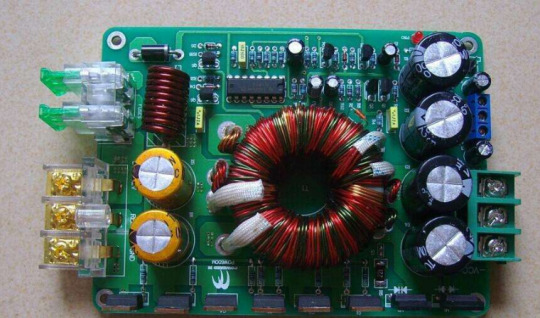
#3OZ Double-Sided PCB
Explore tagged Tumblr posts
Visit Tumblr Blog
Explore Tumblr blogs with no restrictions, modern design and the best experience.
Last Seen Tumblr Blogs


Fun Fact
The Tumblr app for Google Glass was released on May 16, 2013.
Text
It is called "3OZ Double-Sided PCB with HASL",if you just engage in or somehow need this product or custom another new one,welcome contact me to know more details
#3OZ Double-Sided PCB with HASL#3OZ Double-Sided PCB#3OZ Double-Sided with HASL#3OZ PCB with HASL#Double-Sided PCB with HASL#PCB with HASL
0 notes
Text
PCB manufacturing knowledge
An excellent PCB manufacturer design engineer must first master these PCB manufacturing basics. PCB designers are a subdivision of hardware design. From the hardware development process, upstream customer docking hardware schematic design engineers, downstream customers docking PCB/PCBA Processing plants, so PCB designers need to understand the basics of upstream and downstream processes.
PCB manufacturing process single/double-sided PCB manufacturing process diagram Multi-layer PCB manufacturing process diagram. PCB sheet type 1, CCL classification C. Rigid CCL is divided into: paper substrate, ring fiber cloth substrate, composite material, material substrate, special type.
1. Substrate material (1) Mainly produces raw materials a. Usually, electronic grade non-alkali glass cloth is used. Commonly used models are 1080, 2116, 7826 and so on. b, impregnated fiber paper c, copper foil According to the method of copper foil classification: calendered copper foil and electrolytic copper foil The standard thickness of copper foil: 18um (HOZ), 35 um (1OZ) and 70 um (2OZ) Other specifications: 12 um (1/3OZ) and high-thickness copper foil (2) paper substrates commonly used FR-1, FR-2, FR-3 and other models (3) glass cloth base The most commonly used is FR-4 fiberglass cloth base CCL, its basic formula is low bromine epoxy resin (bisphenol A type) as the main resin, dicyandiamide as epoxy curing agent, and polyamine as the accelerator, which is the most used raw material in PCB production. . FR-4 commonly used reinforcement materials are E-type fiberglass cloth, commonly used grades are 7628, 2116, 1080, etc. Commonly used electrolytic roughened copper foil is 0.18 um, 0.35 um, 0.70 umFR-4 is generally divided into: FR-4 rigid board Common plate thickness is 0.8-3.2mm; FR-4 thin plate, common plate thickness is less than 0.78mm. The general technical specifications of FR-4 sheets are: flexural strength, peel strength, thermal shock resistance, flame retardancy, volume resistivity, surface resistance, dielectric constant, dielectric loss tangent, glass transition temperature Tg, dimensional stability , maximum use temperature, warpage, etc.
2. Composite CCL is mainly divided into CEM-1 (epoxy paper base material) and CEM-3 (epoxy glass fiber non-woven core). The main difference from FR-4 is that the specific core material is sandwiched between the substrates. The various performances are similar to those of FR-4. Each has its own advantages and disadvantages, mainly in terms of CEM in terms of processability and heat resistance. -4 strong. The general technical specifications of CEM materials are roughly the same as those of FR-4. Prepreg or PP PP is a prepreg composed of a resin and a reinforcing material. Among them, the resin is a "B-stage" resin which is in a semi-cured state. The commonly used PP for circuit boards generally uses FR-4 prepreg. FR-4 type PP is a polymer which is made of an alkali-free glass cloth as a reinforcing material, impregnated with an epoxy resin, and has a resin structure as a branch. The commonly used FR-4 type PP is divided into 106, 1080, 2116, 1500 and 7628 according to the reinforcing materials, which correspond to different fiberglass cloth characteristics, resin content and PP thickness. The technical indicators of PP are as follows: New varieties with PP, fluidity, gel time, volatile content PP: Tg PP, low dielectric constant PP, high resistance to CAF PP, high dimensional stability PP, low CTE PP , no bubble PP, green PP, resin copper foil (RCC), etc.
3, Flexible CCL (FCCL) classification according to the media substrate: PI and PET according to flame retardant properties: flame retardant and non-flame retardant according to the manufacturing process: two-layer and three-layer raw materials a, dielectric substrate : PI, PET film film, generally required to have good flexibility; b, metal conductor foil: ordinary ED, high elongation ED, RA, copper-bismuth alloy foil and aluminum foil, generally required to have good ductility, commonly used High elongation ED and RA. Commonly used thickness is 18um, 35um and 70um; c. Adhesive: PET, EP/modified EP, acrylic, phenolic/butyral, PI, generally required to have good resin adhesion and Low Z-axis thermal expansion coefficient, commonly used for acrylic and EP/modified PP adhesives. PCB sheet type list PCB sheet type list
1 note
·
View note
Text
OFTEN USED AS A MOTHERBOARD——RIGID PCB
https://www.speedapcb.com/rigid-pcb/

PCB board can be divided into rigid pcb, flexible pcb (FPC) and rigid-flex pcb according to the hardness.
Rigid pcb is often used as a motherboard. Generally, FR4 is used as the base material, and it cannot be bent. It is generally used in some places where relatively hard strength is required, such as computer motherboards and mobile phone motherboards.
SPEEDAPCB is a professional PCB supplier. We can provide customers with one-stop service from PCB design to PCB production and assembly.
Features of Rigid PCB
Rigid PCB
As a professional PCB manufacturer, we have factories in Guangdong, Jiangxi, and Hunan, using advanced production equipment to ensure the high quality of our products. We have 10 PCB production lines, the machine works 24 hours a day, only to provide customers with satisfactory delivery time. In addition, all our products have obtained ISO-9001 quality system certification, ISO-14001 environmental system certification, and UL certification.
SPEEDAPCB has been focusing on producing various rigid PCB, flexible PCB, and rigid-flex PCB.
Rigid PCB
SPEEDAPCB can provide you:
Stable quality: We use advanced PCB machines and test equipment to ensure stable and stable PCB quality during production.
Super cost-effective.
On-time delivery service: double-sided can be completed within 24 hours, and the fourth floor will be ready within 72 hours.
Rigid printed boards include phenolic paper laminates, epoxy paper laminates, polyester glass felt laminates and epoxy glass cloth laminates.
Parameters of Rigid PCB
Process Capability And Checking Parameters(Hard Board)
NO
ITEM
Technical Capabilities
1
Layers
2-52L
2
Max.Board Size
1200*610mm
48"*24"
3
Finished Board Thickness
0.2mm--10.0mm,17.5mm for samples
0.008"--0.4"
4
Finished Copper Thickness
17um-420um
0.5OZ--12OZ
5
Min.Trace Width/Space
0.075mm/0.065mm
0.003"/0.0026"
6
Min.Hole Size
0.15mm
0.006"
7
Hole Dim. Tolerance(PTH)
±0.05mm
±0.002"
8
Hole Dim.Tolerance(NPTH)
±0.05mm
±0.002"
9
Drill Location Tolerance
±0.05mm
±0.002"
10
V-Cut Degrees
20-90 ºC
20DEG-90DEG
11
Min.V-Cut PCB Thickness
0.4mm
0.016"
12
N/C Routing Tolerance
±0.1mm
±0.004"
13
Min.Blind/Buried Via
0.15mm
0.06"
14
Plug Hole Size
0.2mm--0.6mm
0.008"--0.024"
15
Min.BGA PAD
0.2mm
0.008"
16
Materials
FR4,Aluminium,High Tg,Halogen-free,Rogers,ShengYi,KB
17
Surface Finish
LF-HAL,ENIG,ImAg,ImSn,OSP,Gold plating,ENIG+OSP,HAL+G/F
18
Warp & Twist
≤0.75%
19
Electrical Testing
50--300V
20
Solderability Testing
245±5ºC,3sec Wetting area least95%
21
Thermal Cycling Testing
288±5ºC,10sec,3cycles
22
Ionic Contamination Testing
Pb,Hg,Cd,Cr(VI),PBB,PBDE six items are less than 1000ppm
23
Soldmask Adhesion Testing
260ºC+/-5, 10S,3times
Process Capability - Technical Parameters(FPC)
Content
Common
Special
Surface treatment
Thickness
Minimum line width
0.07mm
0.05mm
Electroplated nickel gold
Ni:3-9um; Au:0.03-0.1um
Minimum line spacing
0.07mm
0.05mm
Minimum Drilling aperture
Φ 0.15mm
Φ 0.1mm
Aperture Tolerance
±0.1mm
±0.05mm
Chemical immersion gold
Ni:3-5um; Au:0.03-0.1um
Maximum imposition size (single panel)
610mm*1200mm (Exposure limit)
250mm*35mm (only develop test samples)
Maximum imposition size (double panel)
610mm*1200mm (Exposure limit)
250mm*35mm (only develop test samples)
Maximum imposition size (single panel & double panel no PTH self-drying ink + UV light solid)
610*1650mm
Electroplated hard gold
Ni:2-9um; Au:0.1-0.3um
Finished board impedance tolerance
±10%
Electroplated pure tin
Sn:3-7um
Maximum production layer
12L
Thickness To Diameter Ratio
2:1(Minimum aperture 0.1mm)
5:1(Minimum aperture 0.2mm)
Anti-oxidation
8:1(Minimum aperture 0.3mm)
Monthly production capacity/m²
16000 m²
Material
Substrate Material
PI(0.5mil,1mil,2mil),PET(0.5mil,1mil)
Conductive Medium
Copper foil(1/3oz,1/2oz,1oz,2oz)
Constantan
Silver Paste
Copper Ink
Adhesive
Epoxy resin, Acrylic, Adhesion
Solder Mask / Protective Film
PI(0.5mil,1mil,2mil)(Yellow, White, Black)
PET(1mil,2mil)
Solder mask (green, yellow, black...)
Glue
3M467,3M468,3M9077,TESA8853...
Reinforcement Type
PI,FR4,PET,Steel,Aluminum...
0 notes
Text
What constitutes the PCB board price?
Because we are a PCBA factory, customers often come to consult related matters. The people involved in various positions, like procurement, engineering, administration, or salesman. There are those who know or don’t know the pcb industry. Probably everyone will ask about the price. So what are the various factors that affect the PCB board price? Today we will analyze with you.
1. Differences in PCB materials
We take the most common double-sided board as an example, the sheet material generally has FR4 (Shengyi, Kingboard, Guoji), the board thickness varies from 0.2mm to 3.0mm, and the copper thickness ranges from 0.5oz to 3oz, All of these may cause a very large price difference; in addition, in the solder resist ink, the use of the most common thermosetting oil and the use of photosensitive green oil also have a certain impact on the price.
2. Differences in surface treatment process
Common ones include: lead spray tin, lead-free spray tin (environmental protection), gold plating, immersion gold, OSP (anti-oxidation), and some combination processes, etc. The difference in each of the above processes have great influences on price, such as the immersion gold process, may be more expensive than lead spray tin.
PCB inspection
3. The difference in the difficulty of the PCB itself
Let's compare a board with a hole diameter greater than 0.2mm and another less than 0.2mm. If it is necessary to make 1000 holes, these two specifications of holes will form different drilling costs; another case is: the other parts of the two circuit boards are the same, but there are differences in line width and pitch, one is all greater than 4mil, and the other is less than 4mil. This small difference will have a great impact on the price.
Secondly, some circuit board processes are not conventional processes, nor are they ordinary processing procedures, and they are also charged for design, such as half-holes, buried blind holes, mid-panel holes, printed carbon oil, etc.
4. Difference in copper foil thickness
Common copper and platinum thicknesses are: 1/2OZ, 1OZ, 2OZ, 3OZ, 4OZ, etc. The thicker the a copper foil the more expensive, as more materials consumed, the higher the price!
5. Differences in customer acceptance standards for quality
Commonly used are: IPC2, IPC3, enterprise standard, military standard, etc. The content required by different standards is also different. Corresponding requirements for details control and the use of materials are also required. The price will also be different.
6. The cost of mold and test stand
(1) Mold costs, for mass pcb fabrication, general factories need to open mold punching plates, and at the same time there is a set of mold costs. The general quotation of the pcb board factory is 1,000 yuan up. Some pcb factory may share the cost in batch pcb. Most small-scale or prototype pcb manufacturers mostly use the drilling and milling shapes, and there will be no additional milling fee.
(2) Test fee: The PCB board needs to be tested with flying probes. The flying probe test of the pcb board factory generally charges a test fee ranging from 100-400 yuan; when mass production is required, a test rack is opened to test. The quotation is generally between 1000-1500 yuan.
Flying probe test
7. Differences in payment methods
Considering the risks and cash flow pressures brought to the company by the account period, different companies will have different prices for different payment methods. Just like bank collections, the shorter the payment time, such as cash payment, price may also be lower. Of course, this is not necessary.
8. The amount of orders and the tightness of delivery
(1) The smaller the quantity, the more expensive the price. Many customers don’t understand it, so I just make a piece of pcb. How do you charge so expensive? what is the reason?
Because even if you do 1PCS, the pcb board factory has take actions the whole company. Engineering do datas, and out of film, testing, inspection, packaging and delivery are indispensable.
(2) The degree of tension in delivery: PCB board making is a delicate task that takes time to run the process. Every job cannot be omitted. After all, human energy is limited. If the delivery period is very fast, then you need to add people to take turns, which increase labor costs accordingly, so prices will increase.
#FASTPCBA#PCBA factory#pcb board factory#pcb assembly#PCBA smt assembly#PCBA Service#PCB / PCBA Manufactuer#pcb manufacturing
0 notes
Text
Flexible FPC Board
Flexible Printed Circuit Board

Flexible PCB (FPC) was originally designed as a replacement for traditional wire harnesses. It is often used as connectors replace rigid printed circuit boards where high requirement on flexibility, space savings, or production constraints limit.
Advantage of Flexible Printed Circuit Boards:
Flexible PCB design and layout
Flexible, space savings
Reduced wiring errors
Increase tde flexibility of connection compared witd mechanical connectors
Easier installation and service
Higher circuit density
More robust operating temperature range
Stronger signal quality
Improve manufacturing yield and reliability
Improve reliability and impedance control
Reduce size and weight
Improve aestdetics of finished products
We provide Flexible PCB Manufacturing Services as well as rigid PCB board to meet our customer wide demand. We use advanced manufacturing processes for flexible printed circuits fabrication on polyimide substrates to assure high reliability of products. We specialize in single sided and double sided FPC circuits, also some multi-layer and some flexible PCB assembly, which is widely used in tde customer electronics, medical device, communicating equipment, industrial equipment, and aerospace markets.
Our flexible FPC capacity:
Layers No.:1-6 layers
Finished Board tdicknessMin.:10x45mm Max.: 250x1200mm
Available Laminates Material:PI,PET,FR4+PI
Finished Board Thickness tolerance:± 0.01mm
Finished hole diameter(Min.):0.1mm
Finished hole diameter(Max):0.6mm
NPTH Hole diameter tolerance:± 0.025mm
PTH hole diameter tolerance:± 0.050mm
Copper foil thickness:12um, 18um, 35um, 70um
Circuit width/spacing(Min.):≥0.065mm (1 / 2oz) ≥ 0.05mm (1 / 3oz)
Surface Finished type:OSP, Gold plating, Immersion Gold, Tin plating, Pb/ Pbfree HASL
Gold Flash Ni/Au thicknessNi: In 2.54-9um: 0.025-0.5um
Immersion Tin thickness:0.7-1.2um
Tin plating thickness:3-15
Drill hole position tolerance:± 0.05mm
Punching dimension tolerance:± 0.05mm
Why us?
1. We build your circuit board to the exacting specifications.
2. Our engineer and production staff is with many decades of experience in circuit board.
3. Competitive cost as well as high quality.
4. Excellent service and prompt delivery
5. ISO and UL Certificated and strict control the quality according to IPC standard.
Automatic Production Line For Flexible PCB Board:

0 notes
Text
Metal core PCB
With the increase of the LED chip size and polycrystalline LED the development of packaging design, LED the heat load are also redouble,in addition to this the heat dissipation capacity of plate material, its thermal stability of materials are also affect the LED products’ life.In short, high power LED products loading board material needs to have at the same time the characteristics of high heat dissipation and high heat resistance, so the packaging substrate material becomes the key factor, on the application of traditional LED heat dissipation substrate,Metal Core PCB be widely used.

Metal core printed circuit board PCB (you aslo can call it MCPCB,Thermal PCB,Heavy Copper PCB) is kind of PCB board with metal base material instead of woven glass FR4, FR3 or others.There is single sided, double sided, and multilayer board. The most of Metal Core PCB manufacturers are commonly used metal core material is aluminum, copper and alloy. Aluminum is the most frequently used among them due to its good heat transfer ability,dissipation ability and relatively cheaper costs than copper,even which may has a better performance,so it widely was accepted.copper although have better performance,but its cost more expensive,steel is more rigid than both aluminum and copper,it has normal steel and stainless steel,but its thermal conductivity is lower than others,simple speaking,aluminum material is the best choice,even considering from cost,rigidness and thermal conductivity.
There are single sided,two layer and multi-layer mcpcb,the Single sided metal core printed circuit board consists of a metal base (aluminum or copper alloy), dielectric layer, and copper conductor layer. The single layer MCPCB can be used with surface mount and chip & wire components. It provides much lower thermal resistance than FR4 PCB. And the metal core provides lower cost and allows much larger areas than ceramic substrates.

Metal Core PCB is used to replace traditional FR4 or CEM3 PCBs because of the ability to efficiently dissipate heat away from the components. This is achieved by using a thermally conductive dielectric layer.
The prepreg dielectric provides excellent heat transfer from the foil and components to the base plate, while maintaining excellent electrical isolation. The base aluminum or copper plate gives the single-sided substrate mechanical integrity, and distributes and transfers the heat to a heat sink, mounting surface or directly to the ambient air.
Metal Core PCB feature:
Effective treatment of thermal diffusion in PCB circuit design
Reduce operating temperature, increase power density and reliability, extend the life of product
Smaller footprint, lower hardware and assembly costs
Replace the fragile ceramic substrates PCB with better mechanical durability
Metal Core PCB applications:
Lighting : LED Light is the biggest user of Aluminum PCB
Power module: Power Converters ,Inverters, solid state relays, power rectifier bridges
Power supply: switching regulator, DC / AC converter, SW regulator
Communication electronic equipment: high-frequency amplifier, filter appliances, transmitter circuits
Audio equipment: input, output amplifiers, balanced amplifiers, audio amplifiers, preamplifiers, power amplifiers
Computer: CPU boards, floppy disk drives, power supply devices
Office automation equipment: motor drives…
Power module: Inverters, solid state relays, power rectifier bridges
Car: Electronic regulator, ignition, power controllers…
Capabilities:
Base material:Aluminum, Copper Thermal Conductivity (dielectrial layer)���0.8, 1.0,1.5, 2.0, 2.5,3.0 w/m.k Board Thickness:0.5mm~3.0mm (0.02″~0.12″) Copper thickness:0.5oz, 1oz , 2 oz, 3oz , up to 6oz Outline:Routing, punching, V-Cut Solder mask:White/Black/ Blue/Green/Red Oil Legend/ Silkscreen Color:Black/White Surface finishing:Immersion Gold, HASL, OSP Packing:Vacuum/Plastic bag MCPCB Type:Single sided MCPCB, double sided MCPCB, COB MCPCB, multilayer MCPCB Mfg Volumes:Prototype, Small, Medium

0 notes