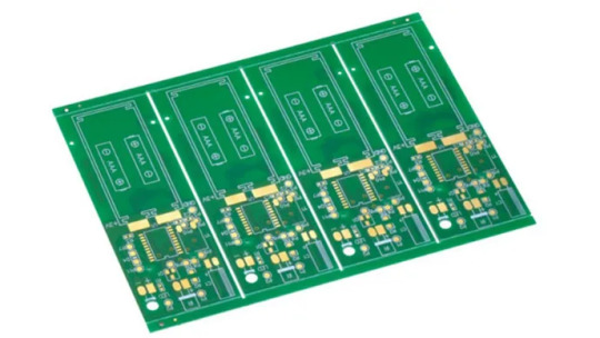
#Double-Sided PCB with HASL
Explore tagged Tumblr posts
Visit Tumblr Blog
Explore Tumblr blogs with no restrictions, modern design and the best experience.
Last Seen Tumblr Blogs


Fun Fact
1,644 Tumblr posts in 1 second.
Text
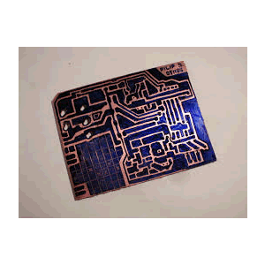
It is called "3OZ Double-Sided PCB with HASL",if you just engage in or somehow need this product or custom another new one,welcome contact me to know more details
#3OZ Double-Sided PCB with HASL#3OZ Double-Sided PCB#3OZ Double-Sided with HASL#3OZ PCB with HASL#Double-Sided PCB with HASL#PCB with HASL
0 notes
Text
Multilayer PCB Materials: Key to Performance and Reliability
In multilayer PCB manufacturing, the choice of materials directly affects electrical performance, thermal stability, and product reliability. Each layer in a multilayer PCB stack-up plays a specific role, and understanding the materials used is essential for optimal design and production.
Core and Prepreg
The foundation of any multilayer PCB is the combination of core and prepreg.
Core is a rigid double-sided laminate made of fiberglass-reinforced resin, usually FR-4, with copper foil on both sides. It provides mechanical strength and supports internal circuitry.
Prepreg is a fiberglass material pre-impregnated with partially cured resin. It is placed between layers during lamination and bonds them together when heat and pressure are applied. Prepreg also serves as insulation between conductive layers.
Common prepreg and core materials include standard FR-4, high-Tg epoxy, polyimide, and halogen-free options.
Copper Foil
Copper is the conductive material that forms the signal layers, power planes, and ground planes in a PCB. It comes in different thicknesses depending on the current requirements. Typical copper thicknesses include 17 microns (0.5 oz), 35 microns (1 oz), and 70 microns (2 oz) per square foot.
There are two main types of copper foil: electrodeposited (ED) copper, which is more economical, and rolled annealed (RA) copper, which is more flexible and used in applications with fine-pitch routing or bending requirements.
Dielectric Materials
Dielectric materials provide electrical insulation between conductive layers. They also influence signal speed, impedance control, and overall board performance.
FR-4 is the most commonly used dielectric in general-purpose PCBs. It is cost-effective and provides adequate thermal resistance for standard applications.
For high-temperature or high-frequency applications, designers often use high-Tg FR-4, polyimide, or PTFE-based materials like Rogers. These advanced materials offer better thermal performance, lower signal loss, and improved stability in harsh environments.
Halogen-free materials are also increasingly popular in eco-friendly and flame-retardant applications.
Solder Mask and Surface Finishes
The solder mask is the colored layer that protects copper traces from oxidation and prevents solder bridging during assembly. Green is the most common color, but others like red, blue, black, and white are also available.
Surface finishes are applied to exposed copper areas such as pads to ensure good solderability and prevent oxidation. Common finishes include HASL (Hot Air Solder Leveling), ENIG (Electroless Nickel Immersion Gold), and OSP (Organic Solderability Preservative).
Material Selection Tips
When selecting materials for a multilayer PCB, engineers consider several factors:
Electrical performance, including signal integrity and impedance control.
Thermal resistance for environments with high operating temperatures.
Mechanical strength and layer count, especially in thicker or rigid-flex designs.
Cost, availability, and compatibility with manufacturing processes.
Choosing the right material combination helps ensure long-term reliability and performance of the final product.
Final Thoughts
Multilayer PCBs are the backbone of modern electronic systems, and material selection is at the core of their success. By understanding the properties and applications of different PCB materials, designers and engineers can make better decisions and achieve more efficient, durable, and high-performance designs.

0 notes
Text
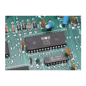
PCB Manufacturing: A Comprehensive Guide to Printed Circuit Board Production

Introduction to PCB Manufacturing
PCB manufacturing is the process of creating printed circuit boards, which are essential components in nearly all modern electronic devices. From smartphones to industrial machinery, PCBs provide the foundation for electrical connections and component mounting. This guide explores the PCB manufacturing process, materials, technologies, and applications.
The PCB Manufacturing Process
1. Design and Schematic Creation
Before production begins, engineers design the PCB using specialized software like Altium Designer, KiCad, or Eagle. The design includes:
Schematic diagrams (circuit connections)
Component placement
Trace routing (copper pathways)
Layer stack-up (for multi-layer PCBs)
Once the design is finalized, a Gerber file (standard PCB manufacturing file) is generated for fabrication.
2. Material Selection
The base material of a PCB is typically FR-4, a flame-resistant fiberglass epoxy laminate. Other materials include:
Flexible PCBs: Made from polyimide for bendable circuits.
High-frequency PCBs: Use Rogers material for RF applications.
Metal-core PCBs: Aluminum or copper for heat dissipation.
3. Printing the Circuit Pattern
The PCB design is transferred onto the board using one of these methods:
Photolithography: A UV-sensitive photoresist is applied, exposed to UV light, and developed to create the circuit pattern.
Direct Imaging: A laser directly etches the pattern onto the PCB.
4. Etching the Copper Layers
After the circuit pattern is printed, the unwanted copper is removed through chemical etching. The remaining copper forms the conductive traces.
5. Drilling Holes for Components
Precision CNC machines drill holes for through-hole components and vias (connections between layers).
6. Plating and Copper Deposition
The drilled holes are electroplated with copper to ensure conductivity between layers.
7. Solder Mask Application
A solder mask (usually green) is applied to protect the copper traces and prevent short circuits. Openings are left for soldering components.
8. Silkscreen Printing
Text, logos, and component labels are printed on the PCB using silkscreen ink for easy assembly and identification.
9. Surface Finish Application
A surface finish is applied to protect exposed copper and improve solderability. Common finishes include:
HASL (Hot Air Solder Leveling)
ENIG (Electroless Nickel Immersion Gold)
OSP (Organic Solderability Preservative)
10. Electrical Testing and Quality Control
Each PCB undergoes automated optical inspection (AOI) and electrical testing to ensure functionality. Defective boards are rejected.
Types of PCBs in Manufacturing
1. Single-Layer PCBs
Simplest and most cost-effective.
Used in basic electronics like calculators.
2. Double-Layer PCBs
Conductors on both sides.
Common in consumer electronics.
3. Multi-Layer PCBs
4+ layers for complex circuits (e.g., motherboards).
Requires precise PCB manufacturing techniques.
4. Flexible PCBs
Used in wearables and medical devices.
Made from bendable materials.
5. Rigid-Flex PCBs
Combines rigid and flexible sections.
Ideal for aerospace and military applications.
Advanced PCB Manufacturing Technologies
1. High-Density Interconnect (HDI) PCBs
Features microvias and finer traces.
Used in smartphones and compact devices.
2. Embedded Components
Passive components (resistors, capacitors) are embedded within the PCB.
Reduces size and improves performance.
3. 3D Printed Electronics
Emerging technology for rapid prototyping.
Combines additive manufacturing with conductive inks.
Applications of PCB Manufacturing
PCBs are used in nearly every industry, including:
Consumer Electronics (Smartphones, Laptops)
Automotive (ECUs, Infotainment Systems)
Medical Devices (Pacemakers, Imaging Systems)
Aerospace & Defense (Avionics, Radar Systems)
Industrial Automation (Robotics, Control Systems)
Challenges in PCB Manufacturing
Miniaturization: Shrinking component sizes demand precision.
High-Speed Signal Integrity: Ensuring minimal interference.
Thermal Management: Preventing overheating in dense circuits.
Environmental Regulations: Compliance with RoHS and REACH.
Future Trends in PCB Manufacturing
AI-Driven Design Optimization
Sustainable Materials (Biodegradable PCBs)
5G and IoT Integration (Higher frequency PCBs)
Automated Smart Factories (Industry 4.0)
Conclusion
PCB manufacturing is a complex yet vital process that powers modern electronics. From design to testing, each step requires precision and expertise. As technology advances, printed circuit boards will continue to evolve, enabling smaller, faster, and more efficient devices.
Whether you're an engineer, hobbyist, or industry professional, understanding PCB manufacturing helps in designing better electronic products for the future.
1 note
·
View note
Text

Hitech’s Capabilities for Copper Based Substrate Manufacturing
Looking for high-performance metal core PCBs with exceptional thermal conductivity and precision engineering? Hitech Circuits has you covered with expert prototyping and small-batch production!
Key Capabilities: • Single / Double side PCBs, up to 1500 × 480 mm • Board thickness: 0.2mm–4.5mm, copper: 18–240μm • Min. hole size: 0.2 mm, hole position tolerance: ±0.075 mm • Fine punching: round holes ≥1.0mm, square slots ≥0.8×0.8mm • V-CUT board thickness: 0.6–3.2mm, angle deviation: ±0.5°
Thermal Performance: • Copper base up to 401 W/(m·K) • Insulation layer up to 38 W/(m·K) • Thermoelectric separation tech: up to 398 W/(m·K) — perfect for ultra-high heat flux designs
Precision & Finish: • Impedance control: within ±8% • Surface finishes: ENIG, ENEPIG, HASL, OSP, and more • Solder mask colors: Green, White, Blue, Red, Matte Black
Production & Delivery: • Capacity: 10,000 m²/month • Lead time: 5–7 days (prototype), 10–14 days (mass production)
Let's bring your thermal-critical projects to life — fast and reliably. Contact us now for a quote! https://www.htmpcb.com/metal-core-pcb-c-10.html
0 notes
Text
Premier Double-Sided PCB Manufacturer in India
As a leading double-sided PCB manufacturer, Vaishnavi Electronics delivers high-quality PCBs designed for complex, high-density circuits. Our advanced manufacturing processes ensure minimal tolerances, providing precision and reliability for your projects. Utilizing premium FR-4 and FR-4 High Tg laminates, our PCBs range from 0.4 to 3.2 mm in thickness and feature finished copper up to 135 microns. We offer various surface finishes, including HAL, HASL, Lacquer, OSP, and ENIG, along with special options like carbon printed contacts and peelable masks. With a production capacity of up to 5000 sq. meters, we efficiently handle orders of all sizes. Elevate your electronic designs with Vaishnavi Electronics' double-sided PCBs.
0 notes
Text

The difference between copper base PCB, fake double-sided copper base PCB and true double-sided copper base PCB
Copper base PCB is the best heat dissipation and the most expensive circuit board among metal-based PCBs. Generally, copper base PCB include single-sided copper PCB, double-sided copper base PCB, and fake double-sided copper base PCB. The specific advantages of copper base PCB make them widely used in areas with large changes in high and low temperatures, as well as in the precision communication equipment and LED car light markets. The pad production processes of copper substrate manufacturers generally include immersion gold, OSP, HASL, immersion silver, etc.
Authenticity of true and false double-sided copper base PCB
Fake double-sided copper base PCB are generally designed by customers with two layers of circuits, but they are not connected to each other. The real double-sided copper base PCB is the double-sided circuit layer designed by the customer with vias connecting the two-sided circuits.
The copper base PCB, circuit layer requires a large current carrying capacity, so a thicker copper foil should be used, with a thickness of generally 35μm~280μm; the thermal conductive insulation layer is the core technology of the copper substrate. The core thermal conductive component is composed of aluminum oxide and silicon powder and a polymer filled with epoxy resin. It has a small thermal resistance (0.15), excellent viscoelastic properties, and is resistant to thermal aging and can withstand mechanical and thermal stress.
The copper substrate metal base is the supporting component of the copper substrate. It is required to have high thermal conductivity. It is generally a copper plate. Copper plates can also be used (copper plates can provide better thermal conductivity). It is suitable for conventional mechanical processing such as drilling, punching and cutting.
The structure of the real and fake double-sided copper substrate can be divided into 5 layers: 1 layer is the top copper foil, 2 layers are thermal conductive insulation materials, 3 layers are aluminum plates, 4 layers are bottom insulation materials, and 5 layers are bottom copper foil. Their functions are as follows:
The 1st layer of copper foil is used as the top circuit pattern (conductive).
The 2nd insulating layer is also the key layer to reflect the thermal conductivity, also known as the thermal conductive layer, which plays a dual role of thermal conductivity and insulation. Whether the heat generated by the LED lamp can be quickly transferred to the aluminum plate, it is necessary to know the thermal resistance of the thermal conductive insulating material.
The function of the 3rd layer is to transfer the heat conducted by the thermal conductive insulating material to the lamp cup again. There is also an installation function.
The functions of the 4th and 5th layers are the same as those of the 2nd and 1st layers above.
Through the above structure, we can easily understand the thermal conductivity and heat dissipation principle of the copper base PCB. In addition, the special process of copper base PCB processing and the thermoelectric separation production technology have improved the thermal conductivity of the copper base PCB by several times. Therefore, most designers who make LED copper base PCB now design a thermoelectric separation thermal conductivity method to make the heat dissipation performance of the copper base PCB better.
Email us Cynthia<[email protected]> if you are interested in PCB and PCBA service.
0 notes
Text
Understanding Double Sided PCBs and Applications
Printed Circuit Boards (PCBs) are the backbone of modern electronics. They are used in almost every electronic device we interact with on a daily basis, from smartphones to home appliances. Among the various types of PCBs, double-sided PCBs are one of the most popular and widely used. In this article, we will discuss double-sided PCBs, their features, applications, and other related aspects.
What are Double Sided PCBs?
Double-sided PCBs are PCBs that have conductive traces on both sides of the board, allowing for more complex circuitry and compact designs. The conductive traces on both sides of the board are connected by small holes called vias. Double-sided PCBs are made of a substrate material, usually FR4, and can have a thickness ranging from 0.2mm to 10mm.
Features of Double Sided PCBs
Double-sided PCBs come with several features that make them an attractive choice for various applications. The most notable features of double-sided PCBs include:
Compact design: Since double-sided PCBs have conductive traces on both sides of the board, they allow for more compact designs, making them an ideal choice for space-constrained applications.
Increased complexity: The ability to have conductive traces on both sides of the board allows for more complex circuitry, making it possible to create more sophisticated electronic devices.
High density: Double-sided PCBs can have high-density circuitry, making them an ideal choice for applications that require high-speed data transmission or high-frequency signals.
Various surface treatments: Double-sided PCBs can be manufactured with a variety of surface treatments, including immersion gold, ENIG, immersion silver/Sn, HASL, and LF-HASL.
Applications of Double Sided PCBs
Double-sided PCBs are widely used in various applications, including:
Consumer electronics: Double-sided PCBs are used in smartphones, tablets, and other consumer electronics due to their compact design and high-density circuitry.
Industrial control: Industrial control systems require PCBs that can withstand harsh environments and provide high-performance features, making double-sided PCBs an ideal choice.
Automotive: Double-sided PCBs are used in automotive electronics due to their ability to withstand high temperatures and vibrations.
Medical devices: Medical devices require PCBs that can provide high-performance features in a compact design, making double-sided PCBs an ideal choice.
Telecommunications: Telecommunications equipment requires PCBs that can handle high-speed data transmission and high-frequency signals, making double-sided PCBs an ideal choice.
Certifications and Delivery Terms
Double-sided PCBs come with several certifications, including UL Consumer (Wear, Electronic Digital, Household Appliances, Connectors)/Industrial Control/Automobile TS16949/Medical/Server, Cloud Computing & Base Station/Aviation/Military/Communication (Certification in Related Applications). Additionally, double-sided PCBs can be delivered using various delivery terms, including DDU, FOB, CFA, CIF, CPT, and EXW.
Conclusion
Double-sided PCBs are an essential component of modern electronics, providing a compact and high-density solution for various applications. With features such as high-density circuitry, increased complexity, and various surface treatments, double-sided PCBs are widely used in consumer electronics, industrial control, automotive, medical devices, and telecommunications. With certifications and delivery terms available, double-sided PCBs provide a reliable and customizable solution for all your electronic needs.
0 notes
Text
Where Can I do FPC Flex PCB Assembly?
https://www.grande-pcba.com/where-can-i-do-fpc-flex-pcb-assembly/Grande has its own PCB Fctory and SMT Assembly factory, which can provide FPC Flex PCB Fabrication and FPC PCBA Manufacturing services!

Flex PCB Assembly Capability
Number of Rigid-Flex PCB / Flex PCB Layers: 10/6;
Minimum Trace Width & Spacing: 3/3mil;
Board Thickness Aperture Ratio: 12:1;
Distance From Hole to Conductor: 6mil;
Impedance Tolerance (Ω): 10%;
Surface Finish: Chemical immersion gold, immersion tin, HASL, hard gold plating, soft gold, silver paste, etc.

Common Types of Flex PCB
At present, Flex PCB has four types: Single-Sided FPC, Double-Sided FPC, Multilayer Flex PCB & Rigid-Flex PCB.
1. Single-Sided FPC: The lowest cost printed circuit board that do not require high electrical performance. In Single-Sided FPC Layout, it has a layer of chemically etched conductive patterns, and the conductive pattern layer on the surface of the flexible insulating substrate is a rolled copper foil. The insulating substrate can be polyimide, polyethylene terephthalate, aramid cellulose ester and polyvinyl chloride.
2. The Double-Sided FPC: A conductive pattern made by etching on both sides of the insulating base film. The metallized hole connects the patterns on both sides of the insulating material to form a conductive path to meet the design and use function of flexibility. The coverlay can protect single and double-sided traces and indicate where the components are placed.
3. Multiayer Flex PCB: To laminate 3 or more layers of single-sided or double-sided FPC together, and form metallized holes by drilling and electroplating to form conductive paths between different layers. In this way, no complicated soldering process is required. Multilayer circuits have huge functional differences in terms of higher reliability, better thermal conductivity and more convenient assembly performance. When designing the layout, the mutual influence of assembly size, number of layers and flexibility should be considered.
4. The traditional Rigid-Flex PCB: Be composed of rigid and flexible substrates selectively laminated together. The structure is tight, and the metallized hole L forms a conductive connection. If a printed board has components on the front and back sides, rigid flexible circuit boards are a good choice.But if all the components are on one side, it will be more economical to choose a double-sided flexible circuit board and laminate a layer of FR4 reinforced material on its back.
5. The FPC flex circuit board with hybrid structure is a multi-layer board, and the conductive layer is made of different metals. An 8-layer board uses FR-4 as the inner layer medium and polyimide as the outer layer medium. Leads extend from three different directions of the main board, and each lead is made of a different metal. Constantan alloy, copper and gold are used as independent leads. This kind of hybrid structure is mostly used in the relationship between electrical signal conversion and heat conversion and under low temperature conditions where the electrical performance is relatively harsh. It is the only feasible solution. It can be evaluated by the convenience of the internal connection design and the total cost to achieve the best performance-price ratio.

https://www.grande-pcba.com/where-can-i-do-fpc-flex-pcb-assembly/
0 notes
Text
Double Sided PCB
The double-sided PCB is more complicated than single-sided PCB. The circuit patterns, on its both sides, are connected through a through hole in the middle. Various types of double-sided PCB are in the market, such as double-sided metal base PCB, high Tg thick copper foil PCB, high-frequency PCB and hybrid dielectric base high-frequency double-sided PCB. Double-sided PCBs are widely used in high-tech industries like telecommunications, power supply, computers, industrial control, digital products, scientific and educational equipment, medical equipment, automobiles, aerospace defense.
The production process of double-sided PCB
Double-sided PCB is usually made of epoxy glass cloth copper-clad laminates. It is mainly used for communication electronic equipment, advanced instruments and electronic computers with high-performance requirements.
The production process of double-sided PCB can be generally divided into several methods, such as process wire method, hole plugging method, masking method and pattern plating-etching method.
Advantages of double-sided PCB
It makes it relatively easy to add conductive paths on the board, which means you will have a PCB that better suits your needs.
As both sides are conductive, a large number of ICs and components can be assembled at any time.
You can add more components as needed as there is an extra layer.
More space and flexible design allow the PCB to suit your requirements.
Double-sided PCB is ideal for demanding applications and advanced electronics.
If necessary, the size of the double-sided PCB can be reduced, because double sides can be used.
This type of PCB may save you money because you may only need one.
Double-sided PCBs can be used in many different applications and electronic products, suitable for a wide range of industries.
The difference between double-sided PCB and single-sided PCB
Appearance. A single-sided PCB only has one layer, but the double-sided PCB has 2 layers, with via hole connecting double-sided PCB circuit.
Different production processes. The two-sided PCB has a copper sink process, which is for the two-sided circuit conduction.
Parameters of double-sided PCB
Material: FR-4
Layers: 2L
Thickness: 1.6mm
Min.Hole Size: 0.3mm
Min.line Width: 0.127mm
Inner Layer Copper Thickness: 35μm
Outer Layer Copper Thickness: /
Surface Finish: OSP, HASL, HASL LF, Immersion Gold, ENIG
Min.Clearance of Hole to Line: 0.127mm
If you have questions about our double-sided PCB production capacity, or the specifications required for your custom project are not listed on this page, please feel free to contact us. We will reply within one workday. We will continue to provide quotation support and design support. Welcome to learn about our production process.
https://www.zfpcba.com/products/double-sided-pcb.html

0 notes
Text
Hot-Selling HASL Lead-Free Double-Sided Circuit Board PCB
With the help of various marketing activities and broadcasting channels, the sales volume of our high-tech and high-quality Digital Satellite Finder LCD Display PCBA, Matte Black Solder Mask Circuit Board, Medical Device PCB has increased significantly. The R&D, design and production of each of our product focuses on technological innovation and precision manufacturing, strictly controlled in accordance with the quality management system to ensure the performance and quality of each factory equipment. Our goal is to provide high quality products at competitive prices, and top-notch service to customers around the world. We have now won a good reputation for outstanding customer service among our overseas customers. Our products are selling well both in domestic and foreign markets.To get more news about BT PCB, you can visit pcbmake official website. Owning high-quality products is the basic guarantee for the continuous development of the company. We always pay attention to the continuous development of the Hot-Selling HASL Lead-Free Double-Sided Circuit Board PCB industry, strive to be the industry leader, and provide customers with the most cost-effective products. We are sticking to excellent quality, competitive price and punctual delivery and better service, and sincerely hope to establish long-term good relationships and cooperation with our new and old business partners from all over the world. We warmly welcome to establish long-term friendly cooperative relations with like-minded and consistent businessmen to create a better future together!
0 notes
Text
Top Double Side PCB Manufacturer in India – Vaishnavi Electronics
Vaishnavi Electronics, a leading double side PCB manufacturer in India, offers high-quality PCBs with advanced specifications to meet diverse electronic requirements.
Vaishnavi Electronics stands out among double side PCB manufacturers in India, delivering superior quality printed circuit boards designed for complex and high-density circuits. Our double-sided PCBs are manufactured using premium FR-4 and FR-4 High Tg laminates, with thicknesses ranging from 0.4 to 3.2 mm. We offer finished copper thicknesses up to 135 microns, ensuring robust and reliable connections. Our precise manufacturing capabilities allow for a minimum track width and spacing of 0.17 mm (7 mil), and hole diameters as small as 0.2 mm (16 mil). Surface finishing options include HAL, HASL, Lacquer, OSP, and ENIG, with special finishes like carbon printed contacts and peelable masks available to suit various application needs. With a production capacity of up to 5000 sq. meters, we are equipped to handle both small and large-scale orders efficiently. Choose Vaishnavi Electronics for your double-sided PCB requirements and experience unparalleled quality and service.
Sources
1 note
·
View note
Text
PCB Fabrication China
When ordering PCB to a producer, apart from PCB design recordsdata fabrication notes can be requested by the producer to finalize the production design and plans. The title is derived from the usage of waves of molten solder to connect steel parts to the PCB. The via-in-pad course of supports extra expertise on fewer layers, proving that greater isn't all the time higher. By using HDI technology, designers now have the choice to place extra elements on both sides of the raw PCB. For more details about digital design companies visit for all the product and service we offer. In low to reasonable portions the fee distinction between ENIG and HASL won't be a lot. For a complete run down on PCB Fabrication China go to http://zaponchina.com/pcb-fabrication/.
TechnoTronix , one of many kingpins in providing tailored PCB prototype has a versatile method to use technical expertise and machines with moderate technologies which proves the reliability to load the undertaking on the proper time and economic system.
One can also take the help of internet in an effort to search such service suppliers. The method is way faster and might create a better quality product than manual soldering of parts. Additional price would be charged for the PCB with gold area covers greater than 15%, but the gold space may only be calculated after file been checked, hope you can understand. I dug round on the internet and DIY PCB fabrication for very small components seems quite tough; most people use house PCBs to make larger circuits out of via-gap components. Figuring out the half number and revision (REV) stage of the drawing is essential. For info on PCB Fabrication China go here.
SMYRNA, GA - More than 2,500 PCB designers , fabricators and assemblers registered for Digital Printed Circuit Board ( ), the business's solely virtual trade present and convention, which is taking place this week. All of our lead-free PCB solutions usually are not solely RoHS initiative compliant, however they offer the same wonderful product quality and customer service you've got come to count on from ETAG Circuits. In response to the continued support for the RoHS initiative, ETAG Circuits has a number of offerings to satisfy your lead-free PCB assembly needs. The aluminium pcb is ideally suited to the mounting of high power light emitting diodes (LEDs) simply dissipating the heat generated by 1W, 3W etc energy gadgets. In order that they want to pay attention to the limitations of the PCB fabrication course of.” More often than not, EI engineers will be capable to change or modify the design; in any other case, the designer has to make the mandatory design modifications.
Large I/ necessities and signal transmission high quality have emerged as key issues for the semiconductor packaging business, as have the assembly process requirements and the ultimate finish of PCB substrates used to achieve dependable interconnections each within IC packages and for the second stage packaging of devices onto PCB substrates.
Nonetheless, thus far this appears to be like like a reasonably feasible methodology for breakout board fabrication. If you haven't yet taken steps to get an perception into a fabrication surroundings, may we once more stress the advantage of visiting a board fabricator, and taking a look at real processes and equipment - there is no such thing as a substitute for sensible experience. Improved thermal conduction leading to versatility in part and monitoring format enabling PCB dimensions to be lowered. PCB has turn out to be a base component for any kind of fabrication processes adopted in all the dominant industries across the globe. A dielectric materials is a substance that may be a poor conductor of electricity, and used as an insulating layer in the PCB build up. Porcelain, mica, glass, plastics and some metal oxides are good dielectrics.
As an trade leader in advanced expertise PCB manufacturing, now we have a company-extensive dedication to steady improvement: consistently reviewing and reassessing our gear and methodologies to note where we're succeeding, and where we can do even better.
This paper basically didn't work for me; it will glue itself to the iron after which separate from the PCB or decide it up as properly. We have now developed and produced plastic part for merchandise range from Electronics, automotive industry, plastic packaging, medical equipment and more. Even though powerful, Prototype PCB cross section evaluation is considered one of a lot of sources for approaching deficiencies on a PCB. The method makes use of a tank to carry a quantity of molten solder; the parts are inserted into or placed on the PCB and the loaded PCB is passed throughout a pumped wave or waterfall of solder. Progressively the notion of ‘By Hole Approach' got here into image to produce a double sided PCB. ETAG COprovides consigned meeting companies for electronics manufacturers in small quantity NPI format.
Easy designs and low thermal impedance of the dielectric out performs all different PCB insulators for energy and excessive-operating temperature parts. We do that by creating the absolute best quality boards and assembly locations, providing excellent customer service and by steady improvement in tone and efficiency. The net impact is the savings on the unit price and time taken to produce this protect commercially. Photo software high quality, laminate prep and imaging parameters are necessary for successful process.
Our highly expert engineers and state-of-the-art equipment enable us to deliver solutions which are optimized for functionality and manufacturability. We're happy with our profitable observe report to this point and that our purchasers are happy with our fine PCB high quality, on-time supply, truthful pricing and superior service.
Facing of the overall unit price of OEM decline, the corporate chooses the requirements of the printing equipment will in keeping with their merchandise, printing tools can fully meet the manufacturing wants of the premise, that may be a price-efficient products.
We consistently share PCB making inspirations, PCB format suggestions and PCB news on our weblog to maintain you informed of any developments in PCB Business. That is essential for both plated and non-plated holes, as non-plated holes might both cut into an adjoining trace or cause shorts during assembly. Care have to be taken when dealing with or re-working the PCB's to avoid micro-cracks within the materials which may permit moisture into the PCB inflicting de-lamination concerns later within the meeting process.
These boards are also in style as wiring circuit boards for the tracts on them are etched with copper due to the steel's excessive conductivity and the procedure wherein components are fixed on board and the electrical energy conducting tract is etched and generally known as PCB meeting.
Due to this, it is acknowledged in the scope of IPC 9121-2016 that readers are inspired to submit course of problems, with photographs, in addition to proposed causes and solutions to the IPC 7-24 Printed Board Process Effects Handbook Subcommittee. Without getting a PCB prototype, the mannequin of a brand new invention will be of no use if the PCB just isn't in good situation.
The first process in every PCB cross section evaluation is, subsequently, an endeavor to establish the mistakes to be able to as small a area as attainable, whereas using the circuit layout and schematic in partnership with point-to-level electrical examining and specialised methods for example thermal picture decision to establish an issue before the cross section even commences.
These new low-loss dielectric supplies imply larger performance in your high-demand PCB prototypes. Be sure that the fabricator knows the material specifications of the PCB laminate by indicating this within the fabrication drawing. Free design and supply of laser lower solder paste screens for the very best quality meeting. In case you are building a PCB that may operate at a excessive temperature (like an LED board) and also you desire a white soldermask then you should also specify a non-browning sort.
As a way to obtain low cost and mass manufacturing, our production facility is relay on well-known and reliable EMS, and contacts manufacturing from China. Multiple through processes, including through in pad and blind via know-how, enable designers more PCB actual estate to put components which might be smaller even closer together. When you need your circuit boards sooner fairly than later, we offer an unique 1 day turnaround service where we'll get your circuit boards to you the subsequent day. Solder placement will be controlled via the use of a exact stencil template for the person PCB being fabricated, to use the fabric only where wanted. Tons of of points associated to the manufacturing and fabrication of printed circuit boards are detailed in the remainder of the doc, in the same style as above. I lately went through our customary set of notes and did a ton of analysis to see what's best.
youtube
2 notes
·
View notes
Text
Double Sided PCB prototyping FR4 2-layer PCB fast turn
Name:Double Sided PCB Material:FR4, CEM-1, Rogers Board thickness:1.6mm Surface treatment:Immersion Gold, ENIG, Immersion silver/Sn, HASL, LF-HASL, OSP Technology:Min Track/Width 3/3mil Payment: L/C,T/T,Western Union Certification:UL Consumer (Wear, Electronic Digital, Household Appliances, Connectors)/Industrial Control/Automobile TS16949/Medical/Server, Cloud Computing & Base Station/Aviation/Military/Communication (Certification in Related Applications) Delivery Term:DDU, FOB, CFA, CIF, CPT, EXW
Two-sided PCB model, the foremost normally surface treatment is HASL. At constant time, OSP, gold plating, immersion gold, immersion silver, is equally applicable.
HASL- sensible appearance, simple to weld tin on the pad, easy welding, low price.
ENIG- stable quality, sometimes employed in the case of boding IC.
For two sided board, using through hole within the middle connects two-sided traces, and there are 2 more processes than single aspect board, that is Electroless Copper and plating.
Double sided boards are wide used and relatively easy, each manufacturer can do, that the competition is usually on the price.
Some makers use low grade CCL, soldermask ink is also comparatively low cost, even the surface plating is skinny, leading to price variations.
At Rocket PCB, we have been using top-grade materials, never cut corners, quality is first-class, our strategy is tiny profits but fast turnover, therefore within the premise of quality assurance, our PCB price is extremely competitive, you’re welcome to inquiry here to get quick quotation!
0 notes
Text
Common Types of Flexible Circuit Board ( FPC )
At present, FPC basically includes four types: Single-sided FPC, Double-sided FPC, Multilayer FPC and Rigid-flex FPC;
Single-sided FPC
Single-sided FPC is the lowest cost printed circuit board that do not require high electrical performance. For single-sided wiring, a single-sided flexible circuit board should be used. It has a layer of chemically etched conductive patterns, and the conductive pattern layer on the surface of the flexible insulating substrate is a rolled copper foil. The insulating substrate can be polyimide, polyethylene terephthalate, aramid cellulose ester and polyvinyl chloride.

Double-sided FPC
The double-sided FPC is a conductive pattern made by etching on both sides of the insulating base film. The metallized hole connects the patterns on both sides of the insulating material to form a conductive path to meet the design and use function of flexibility. The cover film can protect single and double-sided traces and indicate where the components are placed.

Multilayer FPC
Multi-layer FPC is to laminate 3 or more layers of single-sided or double-sided FPC flexible circuit boards together, and form metallized holes by drilling and electroplating to form conductive paths between different layers. In this way, there is no need to use a complicated welding process. Multilayer circuits have huge functional differences in terms of higher reliability, better thermal conductivity and more convenient assembly performance. When designing the layout, the mutual influence of assembly size, number of layers and flexibility should be considered.

Rigid-flex FPC
The traditional rigid-flex circuit board is composed of rigid and flexible substrates selectively laminated together. The structure is compact, and the metallization hole L forms a conductive connection. If there are components on the front and back of a printed circuit board, a rigid flexible circuit board is a good choice. But if all the components are on one side, it will be more economical to choose a double-sided flexible circuit board and laminate a layer of FR4 reinforced material on its back.
The FPC flexible circuit board with hybrid structure is a multi-layer board, and the conductive layer is composed of different metals. An 8-layer board uses FR-4 as the inner layer medium and polyimide as the outer layer medium. Leads extend from three different directions of the main board, and each lead is made of a different metal. Constantan alloy, copper and gold are used as independent leads. This kind of hybrid structure is mostly used in the low temperature conditions where the relationship between electrical signal conversion and heat conversion and the electrical performance are relatively harsh, and it is the only feasible solution. It can be evaluated by the convenience of the internal connection design and the total cost to achieve the best performance-price ratio.

Grande Flexible Circuit Board (FPC) Capability
Rigid/flexible PCB layers: 10/6;
Minimum trace width and trace spacing: 3/3mil;
Board thickness aperture ratio: 12:1;
Distance from hole to conductor: 6mil;
Impedance tolerance (Ω): 10%;
Surface treatment: HAL, ENIG, immersion tin, immersion silver, HASL, hard gold plating, soft gold, silver paste, etc.
https://www.grande-pcba.com/
#fpc#flexible circuit board#pcb manufacturing#pcb prototype#Grande#electronics manufacturing services
0 notes
Text
A professional PCB manufacturer in China
A-TECH is a professional PCB manufacturer in China. We know that the market is full of competition for our customers. We can only continue to improve and strengthen self-building to maintain our competitiveness and create more value for global customers. The following is our The core advantages that make us different:
►A-TECH has a complete PCB manufacturing process inside, from inner layer, lamination to different surface treatments, including HASL, HAL (lead-free), OSP and ENIG, which is different from most PCB manufacturers in China who outsource these processes , We control every aspect of production schedule and internal quality, which is why we can provide customers with excellent quality, reliability and fast delivery time.
►A-TECH has many advanced equipment, including vacuum laminator, vacuum etching line (minimum 2 / 2mil line width/spacing), laser direct imaging (LDI) exposure machine, the latest automatic legend printer (minimum legend width 3mil not Need movie) etc.
►Strong production capacity and a wide variety of PCB boards, including rigid FR4 PCB, flexible PCB, rigid-flex PCB, metal core PCB and microwave/RF PCB, technologies include blind and buried vias, pads, counterbores, press fit Hole, half hole, controlled depth wiring, thick copper, mixed material lamination, etc.
►Different from the prototype PCB manufacturer ordered online, the latter requires 100% correct data files for tracking. Our engineering team provides DFM (design for manufacturing) services before manufacturing. We will submit engineering issues to confirm and communicate with customers. Optimize the design or avoid any potential errors.
►Because all PCB production processes are in-house and have a complete production control system, A-TECH can provide fast door-to-door service from small batches to medium batches. For PCB prototypes, the fastest delivery time is 24 hours for double-sided PCBs. It takes 90 hours to ship 4 to 6 layers, and 72 hours for a multilayer PCB with 8 layers or more.
►A-TECH has complete PCB certificates in the industry, including ISO9001:2015, ISO14001:2015, IATF16949:2016, RoHS, UL, etc. Our products and services are 100% guaranteed to comply with IPC-6012 and IPC-A600F standards.
►By owning our PCB manufacturing and assembly plants, we can meet one-stop needs from PCB manufacturing, component procurement to assembly services.
0 notes