#PCB with HASL
Explore tagged Tumblr posts
Visit Tumblr Blog
Explore Tumblr blogs with no restrictions, modern design and the best experience.
Last Seen Tumblr Blogs


Fun Fact
In 2020, 27% of US Tumblr users had an annual household income of over $100,000.
Text
It is called "3OZ Double-Sided PCB with HASL",if you just engage in or somehow need this product or custom another new one,welcome contact me to know more details
#3OZ Double-Sided PCB with HASL#3OZ Double-Sided PCB#3OZ Double-Sided with HASL#3OZ PCB with HASL#Double-Sided PCB with HASL#PCB with HASL
0 notes
Text

How is Aluminum PCB Made?
1. Material Selection: The primary material for Aluminum PCBs is an aluminum alloy, which acts as the base. This is paired with a thermally insulating layer and then a copper foil. The type of aluminum, insulating material, and copper thickness can vary based on the application.
2. Lamination: The layers are laminated together using heat and pressure. This ensures that the copper foil adheres well to the insulating layer, which in turn is bonded securely to the aluminum base.
3. Circuit Pattern Printing: Once laminated, the desired circuit pattern is printed onto the copper foil using a special ink. This ink acts as a protective barrier in the subsequent etching process.
4. Etching: The board is then subjected to an etching solution. This solution removes the exposed copper, leaving behind only the circuit pattern protected by the ink.
5. Drilling: Holes are drilled into the PCB for component leads or vias. This is done using precise CNC machines to ensure accuracy.
6. Surface Finish: To protect the exposed copper circuitry and improve solderability, a surface finish is applied. Common finishes include HASL (Hot Air Solder Leveling), ENIG (Electroless Nickel Immersion Gold), and OSP (Organic Solderability Preservatives).
7. Solder Mask Application: A solder mask is applied over the circuitry, leaving openings only where soldering will occur. This mask prevents accidental solder bridging during assembly.
8. Silkscreen Printing: For ease of assembly, reference designators and other important information are printed onto the PCB using ink.
9. Testing: Before shipping, the PCBs undergo electrical testing to ensure there are no shorts or open circuits.
10. Cutting and Profiling: The PCBs are then cut from the larger panel and profiled to the desired shape.
11. Final Inspection: A thorough visual inspection is done to ensure the PCB meets all quality standards.
The above process is a general overview, and specific processes will vary depending on the manufacturer and the intended application of the PCB.
0 notes
Text
How to Choose the Right PCB Manufacturer for Your Project
When you're developing a new electronic product, one of the most critical decisions you'll make is selecting a printed circuit board (PCB) manufacturer. A high-quality PCB is the backbone of any electronic device, and a reliable manufacturer ensures your designs are brought to life with precision, durability, and performance in mind. But with so many options available, how do you know which one is right for your needs?
In this guide, we’ll walk through the key factors to consider when choosing a PCB partner, what makes a manufacturer stand out, and how to avoid common pitfalls. Whether you're a startup working on a prototype or an established company moving into mass production, this article will help you make an informed decision.
Why Your Choice of PCB Manufacturer Matters
The PCB is not just another component—it’s the heart of your device. Poor-quality boards can lead to product failures, delays in production, and costly revisions. On the other hand, working with the right manufacturer can improve your product’s reliability, speed up development cycles, and even reduce costs.
This is why many professionals in the electronics space invest time in researching and partnering with trusted printed circuit board manufacturers who have a proven track record.
Key Factors to Consider When Choosing a PCB Manufacturer
1. Experience and Specialization
Not all PCB manufacturers are created equal. Some focus on low-volume prototyping, while others are geared toward high-volume production. Depending on your project, you should look for a manufacturer that aligns with your specific needs.
For example, if you're designing complex multi-layer boards, make sure the manufacturer has extensive experience in producing such designs. A company that regularly handles high-frequency or HDI (High-Density Interconnect) boards will be more equipped to handle advanced requirements.
2. Quality Standards and Certifications
Quality assurance is essential in PCB manufacturing. Look for certifications such as ISO 9001, UL listing, or IPC standards compliance. These certifications indicate that the manufacturer follows recognized best practices and quality control protocols.
Ask if they conduct Electrical Testing (E-Test), X-ray inspection, and other reliability tests. A manufacturer that prioritizes quality will always have robust systems in place to ensure each board meets the required specifications.
3. Production Capabilities
It’s crucial to understand the scope of what your manufacturer can offer. Can they handle the board sizes, layer counts, and materials your design requires? What about turnaround times for prototyping or mass production?
A good manufacturer will offer a clear breakdown of their capabilities, including:
Minimum and maximum board sizes
Supported layer counts
Material types (e.g., FR4, Rogers, etc.)
Surface finish options (e.g., HASL, ENIG, OSP)
Lead time flexibility
Having this information upfront helps you determine if the manufacturer can scale with your project’s needs.
4. Customer Support and Communication
Your relationship with a PCB manufacturer should feel like a partnership. Responsive communication and good customer support are essential, especially if issues arise during production.
Choose a company that provides clear, timely responses and is open to discussing your technical concerns. Ideally, you’ll work with a team that’s invested in helping you succeed—not just one that processes orders and moves on.
5. Pricing Transparency
Cost is always a factor, but the cheapest option isn't always the best. Look for manufacturers that provide detailed quotes, including breakdowns of tooling, materials, testing, and shipping. This ensures there are no surprises later.
You should also understand their pricing model—some manufacturers offer better rates for bulk orders, while others specialize in fast-turn prototypes at a premium.
Domestic vs. Overseas Manufacturers
A common question in the selection process is whether to go with a domestic or overseas manufacturer.
Domestic manufacturers often offer faster shipping, better communication, and easier quality control. They may cost more upfront, but the reduced risk and faster turnarounds can make up for it in the long run.
Overseas manufacturers, particularly in Asia, tend to offer lower costs. However, language barriers, longer shipping times, and quality control challenges can be drawbacks, especially for time-sensitive or high-precision projects.
That said, many printed circuit board manufacturers based in the U.S. or Europe now offer the best of both worlds—competitive pricing with high-quality standards and excellent customer service.
Red Flags to Watch Out For
Choosing the wrong PCB partner can result in production delays, increased costs, or even complete project failure. Here are some warning signs to watch for:
Lack of certifications or quality assurance processes
Poor or inconsistent communication
No clear information about production capabilities
Hidden fees or vague pricing
Limited reviews or a poor reputation in the industry
Always do your due diligence—read reviews, request samples, and even visit their facilities if possible.
Questions to Ask Before Committing
Here are some questions to ask when evaluating potential PCB partners:
What industries do you typically serve?
Can you share recent case studies or examples of similar projects?
What testing and inspection processes do you use?
What is your typical lead time for prototypes and production runs?
How do you handle design revisions or errors?
Asking these questions upfront helps set expectations and ensures you’re working with a manufacturer that understands your goals.
The Value of Long-Term Partnerships
As your product evolves, having a dependable PCB partner becomes even more valuable. A strong relationship can lead to better pricing, faster response times, and even input on design for manufacturability (DFM). The right printed circuit board manufacturers act not just as suppliers, but as strategic allies in your product development journey.
Final Thoughts
Choosing the right PCB manufacturer can make or break your electronics project. It’s not just about finding someone who can produce your board—it’s about finding a partner who understands your vision, meets your quality expectations, and grows with your business.
Take your time, do your research, and don’t hesitate to reach out to multiple manufacturers before making your decision. When done right, the relationship you build with your PCB manufacturer can be one of the most valuable assets in your entire product development process.
0 notes
Text
Surface Finishes for Multilayer PCBs and Their Impact
Multilayer PCBs are essential in modern electronic systems where high-density routing, signal integrity, and reliability are critical. While inner layers are encapsulated during lamination, the outer layers of a multilayer PCB are exposed for component assembly — making surface finish a key factor in performance and long-term reliability.
Surface finish not only protects the exposed copper but also directly influences soldering quality, component compatibility, and board lifespan, especially in complex multilayer designs.
Why Surface Finish Is Critical in Multilayer PCBs
In a multilayer PCB, especially those with 6, 8, or more layers, outer-layer copper traces and pads are often extremely dense and designed for fine-pitch SMT components such as BGAs, QFNs, or high-pin-count connectors.
A good surface finish must:
Ensure consistent solderability across dense pad arrays
Maintain flatness to support reliable assembly of micro-components
Provide oxidation protection during storage and processing
Be compatible with lead-free reflow profiles
Handle multiple reflow cycles without degradation
Multilayer PCBs often undergo more complex assembly and higher thermal stress, so the surface finish must meet higher standards than simple single- or double-layer boards.
Common Surface Finishes for Multilayer PCBs
1. ENIG (Electroless Nickel Immersion Gold)
The most popular surface finish for multilayer boards, especially in high-density and high-reliability applications.
Provides excellent flatness for fine-pitch components (e.g. BGAs)
Stable during multiple reflow cycles
Compatible with high-speed signals due to smooth surface
Long shelf life, ideal for staged assembly
Slightly higher cost but justified by performance
Widely used in servers, telecom equipment, and aerospace PCBs.
2. OSP (Organic Solderability Preservative)
Preferred for cost-sensitive multilayer boards with fine-pitch components.
Flat surface suitable for automated SMT
Environmentally friendly and lead-free
Lower cost than ENIG
Limited shelf life, requires controlled handling
Not ideal for boards requiring multiple assembly cycles
Often used in consumer electronics and automotive applications.
3. Immersion Silver
Used for multilayer boards requiring high signal integrity or RF performance.
Low surface roughness ensures good impedance control
Suitable for high-frequency multilayer PCBs
Sensitive to tarnishing and handling
Better electrical performance than ENIG in certain designs
Good choice for communication equipment and high-speed digital boards.
4. Lead-Free HASL
Sometimes used in low-cost multilayer boards, but not recommended for very dense designs.
Cost-effective, robust finish
Less flat surface can cause soldering issues on fine-pitch pads
May lead to solder bridging in dense layouts
Acceptable for through-hole or mixed technology boards
Usually applied to industrial control or power-related multilayer PCBs.
Surface Finish Considerations in Multilayer PCB Design
When choosing a surface finish for multilayer PCBs, consider:
Assembly method (SMT vs through-hole, single vs multiple reflows)
Pad density and component type (especially fine-pitch packages)
Signal performance needs (RF, impedance control, etc.)
Environmental factors (RoHS, storage conditions)
Budget vs reliability trade-offs
In many high-reliability or mission-critical multilayer designs, ENIG or Immersion Silver is preferred despite higher cost, due to their consistent performance.
Final Thoughts
The outer layers of a multilayer PCB may seem like a small part of a complex system, but the choice of surface finish can make or break the final product. Whether it's ensuring reliable solder joints for 0.4 mm pitch BGAs, withstanding multiple reflow cycles, or maintaining performance in high-frequency circuits — the right surface finish is critical.
Understanding the relationship between board complexity, material stack-up, and surface treatment is essential for delivering a reliable, high-performance multilayer PCB.

0 notes
Text
PCB Manufacturing: A Comprehensive Guide to Printed Circuit Board Production

Introduction to PCB Manufacturing
PCB manufacturing is the process of creating printed circuit boards, which are essential components in nearly all modern electronic devices. From smartphones to industrial machinery, PCBs provide the foundation for electrical connections and component mounting. This guide explores the PCB manufacturing process, materials, technologies, and applications.
The PCB Manufacturing Process
1. Design and Schematic Creation
Before production begins, engineers design the PCB using specialized software like Altium Designer, KiCad, or Eagle. The design includes:
Schematic diagrams (circuit connections)
Component placement
Trace routing (copper pathways)
Layer stack-up (for multi-layer PCBs)
Once the design is finalized, a Gerber file (standard PCB manufacturing file) is generated for fabrication.
2. Material Selection
The base material of a PCB is typically FR-4, a flame-resistant fiberglass epoxy laminate. Other materials include:
Flexible PCBs: Made from polyimide for bendable circuits.
High-frequency PCBs: Use Rogers material for RF applications.
Metal-core PCBs: Aluminum or copper for heat dissipation.
3. Printing the Circuit Pattern
The PCB design is transferred onto the board using one of these methods:
Photolithography: A UV-sensitive photoresist is applied, exposed to UV light, and developed to create the circuit pattern.
Direct Imaging: A laser directly etches the pattern onto the PCB.
4. Etching the Copper Layers
After the circuit pattern is printed, the unwanted copper is removed through chemical etching. The remaining copper forms the conductive traces.
5. Drilling Holes for Components
Precision CNC machines drill holes for through-hole components and vias (connections between layers).
6. Plating and Copper Deposition
The drilled holes are electroplated with copper to ensure conductivity between layers.
7. Solder Mask Application
A solder mask (usually green) is applied to protect the copper traces and prevent short circuits. Openings are left for soldering components.
8. Silkscreen Printing
Text, logos, and component labels are printed on the PCB using silkscreen ink for easy assembly and identification.
9. Surface Finish Application
A surface finish is applied to protect exposed copper and improve solderability. Common finishes include:
HASL (Hot Air Solder Leveling)
ENIG (Electroless Nickel Immersion Gold)
OSP (Organic Solderability Preservative)
10. Electrical Testing and Quality Control
Each PCB undergoes automated optical inspection (AOI) and electrical testing to ensure functionality. Defective boards are rejected.
Types of PCBs in Manufacturing
1. Single-Layer PCBs
Simplest and most cost-effective.
Used in basic electronics like calculators.
2. Double-Layer PCBs
Conductors on both sides.
Common in consumer electronics.
3. Multi-Layer PCBs
4+ layers for complex circuits (e.g., motherboards).
Requires precise PCB manufacturing techniques.
4. Flexible PCBs
Used in wearables and medical devices.
Made from bendable materials.
5. Rigid-Flex PCBs
Combines rigid and flexible sections.
Ideal for aerospace and military applications.
Advanced PCB Manufacturing Technologies
1. High-Density Interconnect (HDI) PCBs
Features microvias and finer traces.
Used in smartphones and compact devices.
2. Embedded Components
Passive components (resistors, capacitors) are embedded within the PCB.
Reduces size and improves performance.
3. 3D Printed Electronics
Emerging technology for rapid prototyping.
Combines additive manufacturing with conductive inks.
Applications of PCB Manufacturing
PCBs are used in nearly every industry, including:
Consumer Electronics (Smartphones, Laptops)
Automotive (ECUs, Infotainment Systems)
Medical Devices (Pacemakers, Imaging Systems)
Aerospace & Defense (Avionics, Radar Systems)
Industrial Automation (Robotics, Control Systems)
Challenges in PCB Manufacturing
Miniaturization: Shrinking component sizes demand precision.
High-Speed Signal Integrity: Ensuring minimal interference.
Thermal Management: Preventing overheating in dense circuits.
Environmental Regulations: Compliance with RoHS and REACH.
Future Trends in PCB Manufacturing
AI-Driven Design Optimization
Sustainable Materials (Biodegradable PCBs)
5G and IoT Integration (Higher frequency PCBs)
Automated Smart Factories (Industry 4.0)
Conclusion
PCB manufacturing is a complex yet vital process that powers modern electronics. From design to testing, each step requires precision and expertise. As technology advances, printed circuit boards will continue to evolve, enabling smaller, faster, and more efficient devices.
Whether you're an engineer, hobbyist, or industry professional, understanding PCB manufacturing helps in designing better electronic products for the future.
1 note
·
View note
Text
PCB Manufacturing: A Comprehensive Guide to Printed Circuit Board Production

Introduction to PCB Manufacturing
PCB Manufacturing is the process of creating Printed Circuit Boards (PCBs), which are essential components in nearly all modern electronic devices. From smartphones to industrial machinery, PCBs provide the foundation for electrical connections, enabling devices to function efficiently. This guide explores the PCB Manufacturing process, materials used, key technologies, and industry trends.
The PCB Manufacturing Process: Step by Step
The production of Printed Circuit Boards involves multiple stages, each requiring precision and expertise. Below is a detailed breakdown of the PCB Manufacturing workflow.
1. Design and Schematic Creation
Before production begins, engineers design the PCB using specialized software like Altium Designer, Eagle, or KiCad. The schematic defines the electrical connections, while the layout determines the physical placement of components.
2. Printing the PCB Design
Once the design is finalized, it is printed onto a laminate material using a photoplotter, which transfers the circuit pattern onto a film.
3. Substrate Preparation
The base material, typically FR-4 (fiberglass-reinforced epoxy laminate), is cleaned and coated with a photosensitive layer called photoresist.
4. Exposure and Developing
The photoresist-coated substrate is exposed to UV light through the printed film. The exposed areas harden, while the unexposed regions are washed away during the developing stage.
5. Etching the Copper Layers
The board is then immersed in an etching solution (usually ferric chloride or ammonium persulfate), which removes unwanted copper, leaving only the desired circuit traces.
6. Drilling Holes for Components
Precision CNC machines drill holes for through-hole components and vias (electrical connections between layers).
7. Plating and Copper Deposition
A thin layer of copper is electroplated onto the board to strengthen the connections and ensure conductivity.
8. Solder Mask Application
A solder mask (usually green, but available in other colors) is applied to protect the copper traces from oxidation and prevent solder bridges.
9. Silkscreen Printing
Component labels, logos, and reference indicators are printed onto the board using silkscreen printing for easier assembly.
10. Surface Finish Application
To prevent oxidation and improve solderability, a surface finish (such as HASL, ENIG, or OSP) is applied.
11. Electrical Testing and Quality Control
Automated AOI (Automated Optical Inspection) and flying probe testers verify electrical connectivity and detect defects.
12. Final Assembly and Shipping
Once tested, the PCBs are assembled with components (if required) and shipped to manufacturers for integration into electronic devices.
Materials Used in PCB Manufacturing
The quality of a Printed Circuit Board depends heavily on the materials used. Key materials include:
Copper Foil: Conducts electricity and forms the circuit traces.
FR-4 Substrate: Provides mechanical strength and insulation.
Solder Mask: Protects copper traces and prevents short circuits.
Silkscreen Ink: Adds labels and markings for assembly.
Surface Finishes (HASL, ENIG, OSP): Enhances solderability and durability.
Advanced PCB Manufacturing Technologies
As electronics evolve, PCB Manufacturing techniques continue to advance. Some cutting-edge technologies include:
1. High-Density Interconnect (HDI) PCBs
These boards feature microvias, finer traces, and multiple layers, enabling compact designs for smartphones and wearables.
2. Flexible and Rigid-Flex PCBs
Made from polyimide or other flexible materials, these PCBs are used in bendable electronics like foldable phones and medical devices.
3. Multilayer PCBs
With 4 to 50+ layers, these PCBs are essential for complex devices like servers and aerospace systems.
4. Embedded Components
Passive components (resistors, capacitors) are embedded within the PCB, reducing size and improving performance.
5. 3D Printed Electronics
Additive manufacturing is being explored for rapid PCB prototyping, allowing faster design iterations.
Challenges in PCB Manufacturing
Despite advancements, PCB Manufacturing faces several challenges:
Miniaturization: As devices shrink, producing ultra-fine traces becomes difficult.
Signal Integrity: High-speed circuits require precise impedance control.
Thermal Management: Dense PCBs generate heat, necessitating effective cooling solutions.
Environmental Regulations: Restrictions on hazardous materials (lead, halogen) impact manufacturing processes.
Future Trends in PCB Manufacturing
The PCB Manufacturing industry is evolving with new trends:
AI and Automation: Machine learning improves defect detection and process optimization.
Sustainable Manufacturing: Eco-friendly materials and lead-free soldering gain traction.
5G and IoT Demand: High-frequency PCBs are needed for 5G networks and IoT devices.
Additive Manufacturing: 3D printing could revolutionize prototyping and low-volume production.
Conclusion
PCB Manufacturing is a complex yet vital industry that powers modern electronics. From design to final testing, each step requires precision to ensure reliability and performance. As technology advances, Printed Circuit Boards will continue to evolve, enabling smaller, faster, and more efficient electronic devices. Understanding the PCB Manufacturing process helps engineers, designers, and manufacturers stay ahead in this rapidly changing field.
By keeping up with emerging trends and overcoming challenges, the PCB Manufacturing industry will remain at the heart of technological innovation. Whether for consumer electronics, automotive systems, or aerospace applications, high-quality PCBs are indispensable in today’s connected world.
1 note
·
View note
Text
A Comprehensive Guide to Circuit Board Manufacturing: From Design to Production
Circuit board manufacturing is the backbone of modern electronics. Whether it's your smartphone, car dashboard, or industrial machine—every electronic device begins with a printed circuit board (PCB). In this guide, we’ll walk through the complete journey of pcb manufacturing, from design to final production, in a simple and easy-to-understand way.
Step 1: PCB Design and Layout
The process begins with a schematic diagram, which is turned into a layout using CAD software.
Engineers choose materials, layer stack-ups, and routing paths based on the product's function.
Design for manufacturability (DFM) checks are done to ensure the design can be produced efficiently using standard Electronics Manufacturing Services.
Step 2: Preparing the Raw Materials
Copper-clad laminates are the base materials used in pcb manufacturing.
These are cleaned and prepped to ensure they bond well with photoresist and other layers.
Step 3: Imaging and Etching
A light-sensitive film (photoresist) is applied to the copper surface.
UV light is used to expose the circuit pattern onto the board.
Unwanted copper is removed using a chemical etching process, leaving behind the desired tracks for circuit board manufacturing.
Step 4: Drilling and Plating
Precise holes are drilled for component leads and inter-layer connections (vias).
These holes are then plated with copper to create electrical pathways between layers.
Need reliable Electronics Manufacturing Services that deliver precision in every layer? Partner with experts who follow global production standards.
Step 5: Solder Mask and Surface Finish
A protective solder mask is applied over the board to prevent oxidation and short circuits.
Finishes like HASL, ENIG, or OSP are added to the pads to improve solderability.
Step 6: Silkscreen and Final Fabrication
Labels, part numbers, and symbols are printed using silkscreen to assist during component assembly.
The boards are then cut into their final shape using CNC routers or V-cut machines.
Step 7: Electrical Testing and Quality Inspection
Each PCB goes through electrical testing to ensure there are no open or short circuits.
Visual inspections and automated tools are used to check for any surface defects or misalignments.
Quality control is critical at every stage of circuit board manufacturing to ensure high performance.
Conclusion
Understanding the full process of pcb manufacturing helps you make better decisions when choosing the right Electronics Manufacturing Services. From detailed design to strict quality checks, every step matters in ensuring the reliability and function of your electronics. High-quality circuit board manufacturing is key to a successful end product.
Upgrade your electronics with trusted Electronics Manufacturing Services for flawless circuit board production.
Also read:-
Top Trends Shaping the Future of Electronics Manufacturing Services in 2025
0 notes
Text
Innovative PCB Manufacturing & Assembly: From Fabrication to Final Product
Printed Circuit Boards (PCBs) form the backbone of modern electronic devices. From smartphones to industrial automation systems, PCBs are integral to functionality and performance. As technology advances, the need for high-quality PCB Fabrication Company services and efficient PCB Manufacturing Company processes continues to grow. With innovations in PCB Board Assembly, PCB Manufacturing Assembly, and PC Board Assembly, manufacturers can now produce more reliable and high-performance PCBs faster than ever before. This article explores the evolving landscape of PCB Assembly Manufacturer services and how fabrication has become more advanced and efficient.
The Role of a PCB Fabrication Company in Modern Electronics
A PCB Fabrication Company is responsible for transforming design concepts into functional circuit boards. This process includes material selection, layering, etching, drilling, and applying solder masks to ensure optimal circuit connectivity. The accuracy and precision of PCB fabrication are crucial to ensuring that the final product meets industry standards.
Key Aspects of PCB Fabrication:
Material Selection: Using high-quality FR4, polyimide, or ceramic substrates based on application requirements.
Multilayer Design: Creating multi-layered PCBs for complex circuits in modern devices.
Surface Treatments: Applying HASL, ENIG, or immersion silver coatings for better conductivity and longevity.
Quality Assurance: Conducting electrical testing and inspections to detect flaws before assembly.
Advancements in PCB Manufacturing Companies
A PCB Manufacturing Company plays a crucial role in large-scale production. They ensure that every PCB meets strict industry regulations while maintaining efficiency. Advancements in automation, AI-driven quality checks, and eco-friendly production techniques have transformed the PCB manufacturing landscape.
Innovations in PCB Manufacturing:
The Importance of PCB Board Assembly in Electronics
Once the PCB fabrication process is complete, PCB Board Assembly takes center stage. This step involves placing and soldering electronic components onto the board. Depending on the design, manufacturers may use Surface Mount Technology (SMT), Through-Hole Technology (THT), or a hybrid approach.
PCB Board Assembly Methods:
Surface Mount Technology (SMT): Components are mounted directly onto the PCB surface using automated pick-and-place machines, increasing assembly speed and precision.
Through-Hole Technology (THT): Components are inserted through drilled holes and soldered, ensuring strong mechanical bonds suitable for high-power applications.
Mixed Assembly: Combining SMT and THT for a balance of efficiency and durability in complex PCB designs.
PCB Assembly Manufacturer: Ensuring Quality & Reliability
A reliable PCB Assembly Manufacturer ensures that PCBs are assembled with the highest precision and meet industry-specific standards. These manufacturers use cutting-edge assembly lines, including robotic soldering and real-time inspection systems, to maintain the integrity of each board.
Features of a Trusted PCB Assembly Manufacturer:
Automated Optical Inspection (AOI): Identifies defects before finalizing the assembly.
X-Ray Inspection: Used for quality control, especially for complex multilayer PCBs.
Functional Testing: Ensures that the assembled PCB performs according to design specifications.
Batch Scalability: Supports both small prototype runs and large-scale production efficiently.
How PCB Manufacturing Assembly is Evolving
The concept of PCB Manufacturing Assembly refers to the complete process of designing, fabricating, assembling, and testing PCBs. Industry trends are continuously evolving, pushing manufacturers to adopt innovative techniques that improve efficiency and reduce production costs.
Future Trends in PCB Manufacturing Assembly:
Flexible & Rigid-Flex PCBs: Increasing adoption for wearable tech and compact devices.
5G-Ready PCB Designs: Meeting the growing demand for faster wireless connectivity.
Eco-Friendly Production: Minimizing waste and using recyclable materials in PCB production.
AI-Driven PCB Assembly: Reducing defects and optimizing manufacturing processes using machine learning.
In Conclusion
The field of PCB manufacturing and assembly is evolving rapidly, driven by innovation in PCB Fabrication Company services, PCB Manufacturing Company advancements, and state-of-the-art PCB Board Assembly techniques. Whether you are looking for PCB Assembly Manufacturer solutions or streamlined PCB Manufacturing Assembly, selecting the right manufacturing partner ensures high-quality, reliable, and cost-effective PCBs. As technology progresses, we can expect even more groundbreaking improvements in how PCBs are designed, fabricated, and assembled, paving the way for the next generation of electronic devices.
0 notes
Text
Comparison of Immersion Gold and HASL Processes for PCBs
In PCB manufacturing, Immersion Gold and HASL (Hot Air Solder Leveling) are two common surface finishing techniques. Below is a brief comparison of the two:
Process Overview
Immersion Gold: Gold is chemically plated onto the metal surface by immersing the PCB in a gold salt solution, creating a uniform gold layer.
HASL: Tin is applied by melting it and spraying it onto the PCB using high-speed air, forming a tin layer.
Performance Comparison
Electrical Conductivity:
Gold offers superior conductivity compared to tin.
Corrosion Resistance:
Gold has excellent resistance to oxidation and corrosion, while tin is less resistant.
Wear Resistance:
Gold has better wear resistance due to its higher hardness.
Solderability:
Both gold and tin offer good solderability, but gold’s surface is easier to solder.
Appearance:
Gold has a shiny yellow finish, while tin has a silver-white sheen.
Applications
Immersion Gold: Used in high-reliability applications like gold fingers and connectors, where long-term stability is crucial.
HASL: More common in general PCB manufacturing, especially for solder pads and traces, due to its lower cost.
Cost and Environmental Impact
Cost: Gold is more expensive, so immersion gold is costlier than HASL, which uses cheaper tin.
Environmental Impact: Immersion gold requires careful environmental handling, while HASL may face challenges with quality control in dynamic environments.
Conclusion
The choice between Immersion Gold and HASL depends on the specific requirements, such as reliability, cost, and environmental factors. At GREATPCB, we help you select the best option based on your needs to ensure optimal PCB performance.
1 note
·
View note
Text

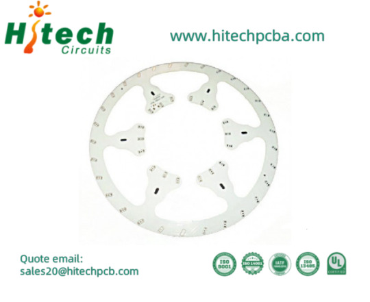
Hitech’s Capabilities for Copper Based Substrate Manufacturing
Looking for high-performance metal core PCBs with exceptional thermal conductivity and precision engineering? Hitech Circuits has you covered with expert prototyping and small-batch production!
Key Capabilities: • Single / Double side PCBs, up to 1500 × 480 mm • Board thickness: 0.2mm–4.5mm, copper: 18–240μm • Min. hole size: 0.2 mm, hole position tolerance: ±0.075 mm • Fine punching: round holes ≥1.0mm, square slots ≥0.8×0.8mm • V-CUT board thickness: 0.6–3.2mm, angle deviation: ±0.5°
Thermal Performance: • Copper base up to 401 W/(m·K) • Insulation layer up to 38 W/(m·K) • Thermoelectric separation tech: up to 398 W/(m·K) — perfect for ultra-high heat flux designs
Precision & Finish: • Impedance control: within ±8% • Surface finishes: ENIG, ENEPIG, HASL, OSP, and more • Solder mask colors: Green, White, Blue, Red, Matte Black
Production & Delivery: • Capacity: 10,000 m²/month • Lead time: 5–7 days (prototype), 10–14 days (mass production)
Let's bring your thermal-critical projects to life — fast and reliably. Contact us now for a quote! https://www.htmpcb.com/metal-core-pcb-c-10.html
0 notes
Text

The difference between copper base PCB, fake double-sided copper base PCB and true double-sided copper base PCB
Copper base PCB is the best heat dissipation and the most expensive circuit board among metal-based PCBs. Generally, copper base PCB include single-sided copper PCB, double-sided copper base PCB, and fake double-sided copper base PCB. The specific advantages of copper base PCB make them widely used in areas with large changes in high and low temperatures, as well as in the precision communication equipment and LED car light markets. The pad production processes of copper substrate manufacturers generally include immersion gold, OSP, HASL, immersion silver, etc.
Authenticity of true and false double-sided copper base PCB
Fake double-sided copper base PCB are generally designed by customers with two layers of circuits, but they are not connected to each other. The real double-sided copper base PCB is the double-sided circuit layer designed by the customer with vias connecting the two-sided circuits.
The copper base PCB, circuit layer requires a large current carrying capacity, so a thicker copper foil should be used, with a thickness of generally 35μm~280μm; the thermal conductive insulation layer is the core technology of the copper substrate. The core thermal conductive component is composed of aluminum oxide and silicon powder and a polymer filled with epoxy resin. It has a small thermal resistance (0.15), excellent viscoelastic properties, and is resistant to thermal aging and can withstand mechanical and thermal stress.
The copper substrate metal base is the supporting component of the copper substrate. It is required to have high thermal conductivity. It is generally a copper plate. Copper plates can also be used (copper plates can provide better thermal conductivity). It is suitable for conventional mechanical processing such as drilling, punching and cutting.
The structure of the real and fake double-sided copper substrate can be divided into 5 layers: 1 layer is the top copper foil, 2 layers are thermal conductive insulation materials, 3 layers are aluminum plates, 4 layers are bottom insulation materials, and 5 layers are bottom copper foil. Their functions are as follows:
The 1st layer of copper foil is used as the top circuit pattern (conductive).
The 2nd insulating layer is also the key layer to reflect the thermal conductivity, also known as the thermal conductive layer, which plays a dual role of thermal conductivity and insulation. Whether the heat generated by the LED lamp can be quickly transferred to the aluminum plate, it is necessary to know the thermal resistance of the thermal conductive insulating material.
The function of the 3rd layer is to transfer the heat conducted by the thermal conductive insulating material to the lamp cup again. There is also an installation function.
The functions of the 4th and 5th layers are the same as those of the 2nd and 1st layers above.
Through the above structure, we can easily understand the thermal conductivity and heat dissipation principle of the copper base PCB. In addition, the special process of copper base PCB processing and the thermoelectric separation production technology have improved the thermal conductivity of the copper base PCB by several times. Therefore, most designers who make LED copper base PCB now design a thermoelectric separation thermal conductivity method to make the heat dissipation performance of the copper base PCB better.
Email us Cynthia<[email protected]> if you are interested in PCB and PCBA service.
0 notes
Text
Multilayer PCB Materials: Key to Performance and Reliability
In multilayer PCB manufacturing, the choice of materials directly affects electrical performance, thermal stability, and product reliability. Each layer in a multilayer PCB stack-up plays a specific role, and understanding the materials used is essential for optimal design and production.
Core and Prepreg
The foundation of any multilayer PCB is the combination of core and prepreg.
Core is a rigid double-sided laminate made of fiberglass-reinforced resin, usually FR-4, with copper foil on both sides. It provides mechanical strength and supports internal circuitry.
Prepreg is a fiberglass material pre-impregnated with partially cured resin. It is placed between layers during lamination and bonds them together when heat and pressure are applied. Prepreg also serves as insulation between conductive layers.
Common prepreg and core materials include standard FR-4, high-Tg epoxy, polyimide, and halogen-free options.
Copper Foil
Copper is the conductive material that forms the signal layers, power planes, and ground planes in a PCB. It comes in different thicknesses depending on the current requirements. Typical copper thicknesses include 17 microns (0.5 oz), 35 microns (1 oz), and 70 microns (2 oz) per square foot.
There are two main types of copper foil: electrodeposited (ED) copper, which is more economical, and rolled annealed (RA) copper, which is more flexible and used in applications with fine-pitch routing or bending requirements.
Dielectric Materials
Dielectric materials provide electrical insulation between conductive layers. They also influence signal speed, impedance control, and overall board performance.
FR-4 is the most commonly used dielectric in general-purpose PCBs. It is cost-effective and provides adequate thermal resistance for standard applications.
For high-temperature or high-frequency applications, designers often use high-Tg FR-4, polyimide, or PTFE-based materials like Rogers. These advanced materials offer better thermal performance, lower signal loss, and improved stability in harsh environments.
Halogen-free materials are also increasingly popular in eco-friendly and flame-retardant applications.
Solder Mask and Surface Finishes
The solder mask is the colored layer that protects copper traces from oxidation and prevents solder bridging during assembly. Green is the most common color, but others like red, blue, black, and white are also available.
Surface finishes are applied to exposed copper areas such as pads to ensure good solderability and prevent oxidation. Common finishes include HASL (Hot Air Solder Leveling), ENIG (Electroless Nickel Immersion Gold), and OSP (Organic Solderability Preservative).
Material Selection Tips
When selecting materials for a multilayer PCB, engineers consider several factors:
Electrical performance, including signal integrity and impedance control.
Thermal resistance for environments with high operating temperatures.
Mechanical strength and layer count, especially in thicker or rigid-flex designs.
Cost, availability, and compatibility with manufacturing processes.
Choosing the right material combination helps ensure long-term reliability and performance of the final product.
Final Thoughts
Multilayer PCBs are the backbone of modern electronic systems, and material selection is at the core of their success. By understanding the properties and applications of different PCB materials, designers and engineers can make better decisions and achieve more efficient, durable, and high-performance designs.

0 notes
Text
Kupferbasierte Leiterplatten sind die teuersten Leiterplatten mit Metallkern, die eine bessere Wärmeleitfähigkeit als Aluminium- und Eisen-basierte Leiterplatten aufweisen und für den Entwurf von Hochfrequenzschaltungen und Bereiche mit großen Schwankungen bei hohen und niedrigen Temperaturen sowie für anspruchsvolle Kommunikationsgeräte und die Architekturdekorationsindustrie verwendet werden. Es gibt alle Arten von kupferbasierten Leiterplatten, wie z. B. Kupfer-Gold-basierte Leiterplatten, versilberte Kupfer-Leiterplatten, Kupfer-Leiterplatten mit Heißluftlötnivellierung (HASL), Kupfer-Antioxidations-Leiterplatten und so weiter.
Kupferbasierte Leiterplatten sind eine Art metallbasierte Leiterplatten, d. h. Leiterplatten aus Kupfersubstrat. Als führende Wärmeleitfähigkeit unter den MCPCBs (Metallkern-Leiterplatten) mit Metallsubstrat weist die Kupferkern-Leiterplatte eine Wärmeleitfähigkeit von bis zu 400 Watt auf. Sie kann die Anforderungen von LED-Lichtquellen mit höherer Leistung nach dem Aluminiumsubstrat erfüllen und verschiedene Wärmeprobleme wie totes Licht mit hoher Leistung, starken Lichtabfall und hohe Wärmeentwicklung lösen.
Als aktivere Starprodukte auf Metallsubstraten haben Leiterplatten auf Kupferbasis und Leiterplatten auf Aluminiumsubstrat ihre Vorteile und werden häufig verwendet. Sie kommen häufig in Autos, Bühnenlichtern, Bedienfeldern, Fotolichtern, Projektionslichtern und Bühnenlaserlampen zum Einsatz und sind hervorragendes Hochleistungszubehör.
0 notes
Text
The Evolution and Advantages of HDI PCB Fabrication in Modern Electronics
The Evolution and Advantages of HDI PCB Fabrication in Modern Electronics
High-Density Interconnect (HDI) Printed Circuit Boards (PCBs) represent a significant advancement in PCB technology, offering enhanced performance and miniaturization for modern electronic devices. As consumer demand for smaller, faster, and more powerful electronics continues to grow, HDI PCBs have become a critical component in meeting these requirements. This article explores the evolution, fabrication process, and advantages of HDI PCB fabrication, highlighting its impact on the electronics industry.Get more news about Hdi PCB fabrication,you can vist our website!
The Evolution of HDI PCBs The development of HDI PCBs has been driven by the need for increased functionality and reduced size in electronic devices. Traditional PCBs, while effective, have limitations in terms of layer count, component density, and signal integrity. HDI technology addresses these limitations by incorporating advanced design and manufacturing techniques that enable higher component density and improved electrical performance.
The evolution of HDI PCBs can be traced back to the 1980s when the first multi-layer PCBs were introduced. Since then, advancements in materials, fabrication methods, and design software have led to the creation of HDI PCBs with multiple layers, finer lines and spaces, and smaller via structures. Today, HDI technology is widely used in various industries, including consumer electronics, telecommunications, automotive, and aerospace.
The HDI PCB Fabrication Process The fabrication of HDI PCBs involves several key steps, each contributing to the overall performance and reliability of the final product:
Design and Layout
The fabrication process begins with the design and layout of the HDI PCB. Advanced design software is used to create detailed schematics and layouts that optimize the placement of components, vias, and traces. Designers must consider factors such as signal integrity, thermal management, and manufacturability during this phase.
Material Selection
The choice of materials is critical for the performance of HDI PCBs. High-quality laminates, copper foils, and prepregs are selected to ensure the board's durability, electrical performance, and thermal stability. The materials must also be compatible with the specific fabrication processes used for HDI PCBs.
Laser Drilling and Via Formation
One of the defining features of HDI PCBs is the use of microvias—small, high-density vias that connect different layers of the PCB. Laser drilling technology is employed to create these microvias with precision and accuracy. Blind, buried, and stacked vias are commonly used in HDI PCBs to achieve higher interconnect density and improved signal performance.
Layer Lamination
The individual layers of the HDI PCB are laminated together using heat and pressure. This process ensures a strong bond between the layers and helps achieve the desired mechanical and electrical properties. The lamination process must be carefully controlled to prevent defects such as delamination or misalignment.
Patterning and Etching
After lamination, the copper layers are patterned and etched to create the desired circuit traces. Advanced photolithography and chemical etching techniques are used to achieve fine line widths and precise trace patterns. The accuracy of this step is crucial for the overall performance of the HDI PCB.
Surface Finishing and Solder Mask Application
The exposed copper traces are coated with a protective surface finish to prevent oxidation and improve solderability. Common surface finishes include ENIG (Electroless Nickel Immersion Gold), HASL (Hot Air Solder Leveling), and OSP (Organic Solderability Preservative). A solder mask is then applied to the board to protect the traces and prevent solder bridging during component assembly.
Inspection and Testing
The final HDI PCB undergoes rigorous inspection and testing to ensure its quality and reliability. Automated optical inspection (AOI), X-ray inspection, and electrical testing are performed to detect any defects or issues. This step ensures that the HDI PCB meets the required specifications and performs as intended.
Advantages of HDI PCBs Increased Component Density
HDI technology allows for higher component density by utilizing microvias, fine lines, and multiple layers. This increased density enables the integration of more components and functionalities into a smaller footprint, making HDI PCBs ideal for compact electronic devices.
Improved Signal Integrity
The shorter signal paths and reduced parasitic effects in HDI PCBs result in improved signal integrity and reduced signal loss. This advantage is particularly important for high-speed and high-frequency applications where signal performance is critical.
0 notes
Text
Hochleistungs-LED-Straßenbeleuchtung – Bergquist Aluminium-PCB
Bergquist Aluminium-Bedruckte Leiterplatte Produkttyp: Aluminium-Leiterplatte Material: Aluminiumplatte + Hochleistungsmaterial mit hoher Wärmeisolierung Lagen/Dicke: 1L/1,0 mm Äußeres Kupfer: 2 OZ Oberflächenbehandlung: HASL LF Lötmaske: Weiß auf einer Seite Technische Merkmale: Bergquist HPL-03015 Anwendung: Lampen und Hochfrequenzverstärker
Website1: https://www.hitechcircuits.com Website2: https://www.hitechpcba.com Website3: https://www.htmpcb.com Email: [email protected] Call/Whatsapp: +86 13302435080
0 notes
Text
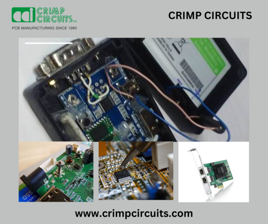
The Journey of PCB Assembly: An Intricate Dance of Precision and Technology
Printed Circuit Board (PCB) assembly is the process of connecting electronic components with the wiring of printed circuit boards. This sophisticated process involves various steps, each crucial for ensuring the functionality and reliability of the final electronic product. From consumer electronics to industrial machinery, PCBs are the backbone of modern technology. In this blog, we will delve into the intricate journey of PCB assembly, highlighting key stages and the technologies involved.
Design and Prototyping
The journey of PCB assembly begins with design and prototyping. Engineers use software like Eagle, Altium Designer, or KiCad to create detailed schematics of the PCB. This design stage involves specifying the locations of components and the routing of electrical connections. The design is then translated into a physical prototype, often through rapid prototyping techniques such as 3D printing or CNC machining.
Material Selection
Selecting the right materials is critical for the performance and durability of the PCB assembly. The board itself is typically made from a fiberglass-reinforced epoxy laminate, known as FR4. The choice of copper thickness, solder mask, and surface finish (such as HASL, ENIG, or OSP) also plays a significant role in the board’s performance and cost.
PCB Fabrication
Once the design and materials are finalized, the PCB fabrication process begins. This involves several steps:
Layering: Multi-layer PCBs are constructed by stacking and bonding multiple layers of copper and insulating material.
Etching: Copper layers are etched to remove unwanted copper, leaving only the desired circuit patterns.
Drilling: Holes for component leads and vias are drilled with precision.
Plating: Holes are plated with copper to ensure electrical connectivity between layers.
Solder Mask and Silkscreen: A solder mask is applied to protect the copper traces, and a silkscreen is added to indicate component locations.
Component Placement
With the PCB fabricated, the next step is to place the electronic components onto the board. This process can be done manually for small-scale or prototype runs, but is typically automated using Surface Mount Technology (SMT) for larger production volumes. Automated Pick-and-Place machines accurately place components onto the PCB at high speeds.
Soldering
After component placement, the components must be securely attached to the board using solder. There are two primary methods for soldering:
Reflow Soldering: For SMT components, solder paste (a mixture of powdered solder and flux) is applied to the board, and then the entire board is heated in a reflow oven. The solder paste melts and solidifies, creating strong electrical and mechanical bonds.
Wave Soldering: For through-hole components, the board is passed over a wave of molten solder. The solder adheres to the exposed metal surfaces, forming connections.
Inspection and Testing
Ensuring the quality and functionality of the assembled PCB is paramount. Various inspection and testing methods are employed:
Automated Optical Inspection (AOI): AOI systems use cameras to inspect the PCB for defects such as missing components or solder bridges.
X-ray Inspection: X-ray machines can inspect hidden solder joints, especially useful for Ball Grid Array (BGA) components.
Functional Testing: This involves powering the PCB and verifying that it performs as expected under operating conditions.
Final Assembly and Packaging
Once the PCB passes inspection and testing, it may undergo final assembly, where additional components such as connectors, heatsinks, or enclosures are added. The completed product is then packaged, ready for shipping to customers or further integration into larger systems.
Conclusion
The journey of PCB assembly is a fascinating blend of design, materials science, precision engineering, and advanced manufacturing techniques. Each stage, from initial design to final testing, plays a crucial role in delivering reliable and high-performance electronic products. As technology continues to evolve, so too will the methods and tools used in PCB assembly, driving innovation and enabling the creation of increasingly sophisticated electronic devices. For more details visit our website www.crimpcircuits.com
#pcb manufacturing toronto#printed circuit board design#metal clad pcb#printed circuits#rigid flex pcb#full turnkey pcb services#turnkey pcb services#pcb parts#eagle software#pcb designing#flexible pcb#pcb assembly#printed circuit board manufacturers#pcb manufacturers in canada#circuit board manufacturers in canada#pcb quote#pcb prototype services in canada
0 notes