#EECE Department
Explore tagged Tumblr posts
Visit Tumblr Blog
Explore Tumblr blogs with no restrictions, modern design and the best experience.
Last Seen Tumblr Blogs


Fun Fact
Tumblr is available in 18 languages.
Text
Quantum simulator could help uncover materials for high-performance electronics
New Post has been published on https://thedigitalinsider.com/quantum-simulator-could-help-uncover-materials-for-high-performance-electronics/
Quantum simulator could help uncover materials for high-performance electronics

Quantum computers hold the promise to emulate complex materials, helping researchers better understand the physical properties that arise from interacting atoms and electrons. This may one day lead to the discovery or design of better semiconductors, insulators, or superconductors that could be used to make ever faster, more powerful, and more energy-efficient electronics.
But some phenomena that occur in materials can be challenging to mimic using quantum computers, leaving gaps in the problems that scientists have explored with quantum hardware.
To fill one of these gaps, MIT researchers developed a technique to generate synthetic electromagnetic fields on superconducting quantum processors. The team demonstrated the technique on a processor comprising 16 qubits.
By dynamically controlling how the 16 qubits in their processor are coupled to one another, the researchers were able to emulate how electrons move between atoms in the presence of an electromagnetic field. Moreover, the synthetic electromagnetic field is broadly adjustable, enabling scientists to explore a range of material properties.
Emulating electromagnetic fields is crucial to fully explore the properties of materials. In the future, this technique could shed light on key features of electronic systems, such as conductivity, polarization, and magnetization.
“Quantum computers are powerful tools for studying the physics of materials and other quantum mechanical systems. Our work enables us to simulate much more of the rich physics that has captivated materials scientists,” says Ilan Rosen, an MIT postdoc and lead author of a paper on the quantum simulator.
The senior author is William D. Oliver, the Henry Ellis Warren professor of electrical engineering and computer science and of physics, director of the Center for Quantum Engineering, leader of the Engineering Quantum Systems group, and associate director of the Research Laboratory of Electronics. Oliver and Rosen are joined by others in the departments of Electrical Engineering and Computer Science and of Physics and at MIT Lincoln Laboratory. The research appears today in Nature Physics.
A quantum emulator
Companies like IBM and Google are striving to build large-scale digital quantum computers that hold the promise of outperforming their classical counterparts by running certain algorithms far more rapidly.
But that’s not all quantum computers can do. The dynamics of qubits and their couplings can also be carefully constructed to mimic the behavior of electrons as they move among atoms in solids.
“That leads to an obvious application, which is to use these superconducting quantum computers as emulators of materials,” says Jeffrey Grover, a research scientist at MIT and co-author on the paper.
Rather than trying to build large-scale digital quantum computers to solve extremely complex problems, researchers can use the qubits in smaller-scale quantum computers as analog devices to replicate a material system in a controlled environment.
“General-purpose digital quantum simulators hold tremendous promise, but they are still a long way off. Analog emulation is another approach that may yield useful results in the near-term, particularly for studying materials. It is a straightforward and powerful application of quantum hardware,” explains Rosen. “Using an analog quantum emulator, I can intentionally set a starting point and then watch what unfolds as a function of time.”
Despite their close similarity to materials, there are a few important ingredients in materials that can’t be easily reflected on quantum computing hardware. One such ingredient is a magnetic field.
In materials, electrons “live” in atomic orbitals. When two atoms are close to one another, their orbitals overlap and electrons can “hop” from one atom to another. In the presence of a magnetic field, that hopping behavior becomes more complex.
On a superconducting quantum computer, microwave photons hopping between qubits are used to mimic electrons hopping between atoms. But, because photons are not charged particles like electrons, the photons’ hopping behavior would remain the same in a physical magnetic field.
Since they can’t just turn on a magnetic field in their simulator, the MIT team employed a few tricks to synthesize the effects of one instead.
Tuning up the processor
The researchers adjusted how adjacent qubits in the processor were coupled to each other to create the same complex hopping behavior that electromagnetic fields cause in electrons.
To do that, they slightly changed the energy of each qubit by applying different microwave signals. Usually, researchers will set qubits to the same energy so that photons can hop from one to another. But for this technique, they dynamically varied the energy of each qubit to change how they communicate with each other.
By precisely modulating these energy levels, the researchers enabled photons to hop between qubits in the same complex manner that electrons hop between atoms in a magnetic field.
Plus, because they can finely tune the microwave signals, they can emulate a range of electromagnetic fields with different strengths and distributions.
The researchers undertook several rounds of experiments to determine what energy to set for each qubit, how strongly to modulate them, and the microwave frequency to use.
“The most challenging part was finding modulation settings for each qubit so that all 16 qubits work at once,” Rosen says.
Once they arrived at the right settings, they confirmed that the dynamics of the photons uphold several equations that form the foundation of electromagnetism. They also demonstrated the “Hall effect,” a conduction phenomenon that exists in the presence of an electromagnetic field.
These results show that their synthetic electromagnetic field behaves like the real thing.
Moving forward, they could use this technique to precisely study complex phenomena in condensed matter physics, such as phase transitions that occur when a material changes from a conductor to an insulator.
“A nice feature of our emulator is that we need only change the modulation amplitude or frequency to mimic a different material system. In this way, we can scan over many materials properties or model parameters without having to physically fabricate a new device each time.” says Oliver.
While this work was an initial demonstration of a synthetic electromagnetic field, it opens the door to many potential discoveries, Rosen says.
“The beauty of quantum computers is that we can look at exactly what is happening at every moment in time on every qubit, so we have all this information at our disposal. We are in a very exciting place for the future,” he adds.
This work is supported, in part, by the U.S. Department of Energy, the U.S. Defense Advanced Research Projects Agency (DARPA), the U.S. Army Research Office, the Oak Ridge Institute for Science and Education, the Office of the Director of National Intelligence, NASA, and the National Science Foundation.
#Algorithms#amplitude#analog#approach#atom#atomic#atoms#author#Beauty#Behavior#change#classical#computer#Computer Science#Computer science and technology#computers#computing#computing hardware#condensed matter#defense#Defense Advanced Research Projects Agency (DARPA)#Department of Energy (DoE)#Design#devices#Discoveries#dynamics#education#effects#Electrical engineering and computer science (EECS)#electromagnetic
1 note
·
View note
Text
The owner of a Cape Cod, Massachusetts home daycare center has closed her business after she was outed for harboring an illegal immigrant—he also happens to be baby daddy to her two children—who was convicted in Brazil for the rape of a 13-year-old girl. Instead of facing justice in his homeland, the child rapist illegally crossed the border into the United States and holed up in the home that housed the daycare center where, presumably, he came into regular contact with the children enrolled in the daycare program.
....
The kicker here is that the state daycare licensing agency, the Department of Early Education and Care (EEC), had inspected Nunes' daycare center five times and failed to discover Tiago Lucas's presence in the home. And Ms. Nunes clearly chose not to alert authorities to the fact that a child predator was in her house and likely had unfettered access to the children in her care.
Absolutely disgusting that this was ever allowed to happen. This is what the left and the Democrats are fighting so hard to defend. If you support them, then this is what you support. Remember this and vote accordingly in all future elections.
38 notes
·
View notes
Text
Foreign Business Act
The Foreign Business Act (FBA) B.E. 2542 (1999) regulates and restricts foreign participation in certain business sectors in Thailand. The purpose of the FBA is to protect local businesses while encouraging foreign investment in targeted areas that benefit the country's economy. Foreign companies must understand the restrictions and licensing requirements outlined in this act to legally operate in Thailand.
1. Structure of the Foreign Business Act
The FBA classifies business activities into three categories (Annexes), each with varying degrees of restrictions:
1.1 Annex 1: Prohibited Activities
Reserved exclusively for Thai nationals, these activities are off-limits to foreigners due to their cultural, historical, or national importance. Foreigners cannot engage in these businesses under any circumstances.
Examples:
Newspaper and media businesses
Rice farming, livestock farming, and forestry
Trading and auctioning of Thai antiques
1.2 Annex 2: Restricted Activities (Subject to Cabinet Approval)
Foreigners can participate in these activities with special approval from the Thai Cabinet due to their potential impact on national security or public welfare.
Examples:
Production of firearms and military equipment
Domestic transportation
Mining and certain types of manufacturing
1.3 Annex 3: Restricted Activities (Requiring a Foreign Business License)
Foreigners may engage in these activities but must first obtain a Foreign Business License (FBL) from the Ministry of Commerce.
Examples:
Retail and wholesale trade
Hotels (excluding hotel management services)
Construction (with certain exceptions)
Legal, accounting, and architecture services
2. Definition of a Foreign Business
A business is considered foreign if it meets any of the following criteria:
It is registered outside Thailand.
More than 49% of its shares are owned by foreign nationals.
Companies with Thai majority ownership (51%) are considered Thai entities and are not subject to FBA restrictions.
3. Obtaining a Foreign Business License (FBL)
3.1 Application Process
Document Submission: Submit the necessary documents, including the business plan, company details, and financial projections, to the Department of Business Development (DBD).
Agency Review: The DBD will evaluate the application based on the business’s contribution to the economy, local employment, and technology transfer.
Approval or Rejection: The review process takes 60–90 days. Approval is granted if the business provides significant benefits to Thailand.
3.2 Criteria for Approval
Economic Contribution: Must provide clear benefits to Thailand's economy.
Local Employment: Businesses that create job opportunities for Thai citizens are favored.
Technology Transfer: Companies introducing new technology have a better chance of approval.
4. Exceptions and Special Cases
4.1 U.S.-Thailand Treaty of Amity
Under this treaty, U.S. citizens and companies can own up to 100% of businesses in most sectors, except those restricted under Annex 1 (e.g., land ownership, media).
4.2 Board of Investment (BOI) Promotion
BOI-promoted companies are exempt from certain FBA restrictions and enjoy tax incentives and easier approval processes.
4.3 Eastern Economic Corridor (EEC)
Businesses investing in high-tech industries within the Eastern Economic Corridor receive additional incentives and reduced restrictions.
5. Penalties for Non-Compliance
Operating a business without the required license can result in:
Fines up to 1 million THB
Imprisonment for up to 3 years
Business closure and forfeiture of profits
6. Recent Developments and Future Trends
Thailand continues to review its foreign business regulations to balance economic development and local business protection. There is growing discussion on liberalizing certain sectors such as technology, e-commerce, and renewable energy to attract foreign investment.
7. Conclusion
The Foreign Business Act is a cornerstone of Thailand’s business environment, regulating foreign participation in key sectors. While the FBA imposes restrictions, it also provides clear pathways for legal operation through licenses, BOI promotion, and bilateral agreements. Foreign investors must conduct thorough research, engage local legal experts, and comply with the FBA’s requirements to operate successfully in Thailand.
#thailand#corporate#business#corporateinthailand#businessinthailand#thai#lawyers#corporatelawyers#businesslawyers#corporatelawyersinthailand#foreignbusinessact#fba
2 notes
·
View notes
Text

Gary Stephen May (born May 17, 1964) is the second African American chancellor of a campus of the University of California.
He was born in St. Louis, one of the two children of Warren May Jr., a postal clerk, and Gloria May, an elementary school teacher. Though raised a Methodist he attended a Catholic elementary school and a Lutheran high school. Selected as a US Presidential Scholar and having participated in a summer program directed by the McDonnell-Douglas Corporation, he was persuaded to enter The Georgia Institute of Technology where he majored in Electrical Engineering, he graduated magnum cum laude in 1988.
He enrolled in the doctoral program in Electrical Engineering and Computer Science at UC Berkeley, completing his Ph.D. with a dissertation titled “Automated Malfunction Diagnosis of Integrated Circuit Manufacturing Equipment.” He was involved with the National Society of Black Engineers, serving as its national chairperson (1987-89).
He returned to Georgia Tech as an EECS assistant professor. Promoted to full professor, he was named the Motorola Foundation Professor of Microelectronics. He was made chairman of EECS when the department was ranked sixth in the nation in that field. He was appointed Dean of the College of Engineering at Georgia Tech, the first African American in that post. He devised a very effective summer program that brought hundreds of such undergraduate students from across the nation to Georgia Tech to perform research and to encourage them to commit to graduate study. He co-created and directed a National Science Foundation-funded program on his campus that significantly increased the school’s students of color doctoral graduates in STEM fields. His known academic works are the books Fundamentals of Semiconductor Fabrication and Fundamental of Semiconductor Manufacturing and Process Control.
He was chosen to become the seventh chancellor of the UC Davis. He and his wife, LeShelle, a former system/ software developer, have two daughters. #africanhistory365 #africanexcellence
2 notes
·
View notes
Text
A new record for Math Prize for Girls wins
Twelfth grader Jessica Wan three-peats, as MIT hosts the 15th competition for female middle and high school math enthusiasts.
Sandi Miller | Department of Mathematics
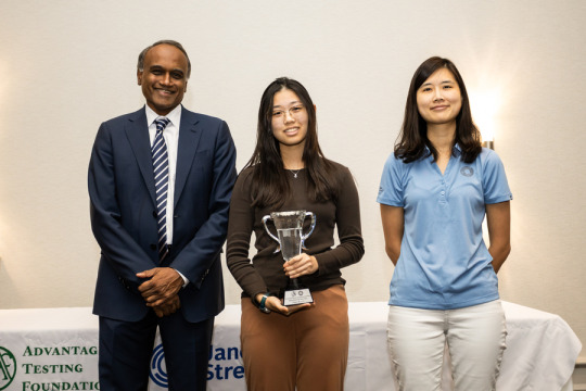
Florida Virtual School senior Jessica Wan was the winner of the 15th Math Prize for Girls (MP4G) annual contest for female-identifying contestants, held Oct. 6-8 at MIT.
She scored 17 out of 20 questions, which added up to make Wan the MP4G’s most successful contestant in its history; she also won the contest last year and in 2019, as an eighth grader. (MP4G paused for two years at the height of the Covid-19 pandemic.) Because Wan had won $82,000 in previous years, she was limited to only earning $18,000 this year by contest rules placing a $100,000 lifetime limit on winnings.
The 262 U.S. and Canadian middle and high school contestants took a two-and-a-half-hour exam that featured 20 multistage problems in geometry, algebra, and trigonometry. Here's an example of one of the questions:
The frame of a painting has the form of a 105” by 105” square with a 95” by 95” square removed from its center. The frame is built out of congruent isosceles trapezoids with angles measuring 45 degrees and 135 degrees. Each trapezoid has one base on the frame’s outer edge and one base on the frame’s inner edge. Each outer edge of the frame contains an odd number of trapezoid bases that alternate long, short, long, short, etc. What is the maximum possible number of trapezoids in the frame?
Hosted by the MIT Department of Mathematics and sponsored by the Advantage Testing Foundation and global trading firm Jane Street, the MP4G weekend culminated in an awards ceremony held at the Marriott in Kendall Square, Cambridge, Massachusetts. MIT electrical engineering and computer science (EECS) Professor Regina Barzilay gave the Maryam Mirzakhani keynote lecture, “Uncovering Mysteries of Life Sciences with Machine Learning.” The event was emceed by MP4G alumna In Young Cho, a quantitative trader from Jane Street who placed third in 2010, and featured a performance by the MIT Logarhythms.
In second place was eighth grader Selena Ge of Jonas Clarke Middle School in Lexington, Massachusetts, with a score of 14 to earn $20,000. She also was awarded a Youth Prize of $2,000 as the highest-scoring contestant in ninth grade or below.
The next four winners were junior Hannah Fox of Proof School in California, who received $10,000 with a score of 12; with scores of 11 each, $4,000 was awarded to sophomores Shruti Arun of Cherry Creek High School in Colorado, Catherine Xu of Iowa City West High School in Iowa, and senior Miranda Wang of Kent Place School in New Jersey. The next 12 winners received $1,000 each.

The top 41 students are invited to take the 2023 Math Prize for Girls Olympiad at their schools. Canada/USA Mathcamp also provides $250 merit scholarships to the top 35 students who enroll in its summer program.
Keep reading.
Make sure to follow us on Tumblr!
5 notes
·
View notes
Text
Atlas of human brain blood vessels highlights changes in Alzheimer’s disease

Atlas of human brain blood vessels highlights changes in Alzheimer’s disease MIT researchers characterize gene expression patterns for 22,500 brain vascular cells across 428 donors, revealing insights for Alzheimer’s onset and potential treatments. Your brain is powered by 400 miles of blood vessels that provide nutrients, clear out waste products, and form a tight protective barrier — the blood-brain barrier — that controls which molecules can enter or exit. However, it has remained unclear how these brain vascular cells change between brain regions, or in Alzheimer’s disease, at single-cell resolution. To address this challenge, a team of scientists from MIT’s Computer Science and Artificial Intelligence Laboratory (CSAIL), The Picower Institute for Learning and Memory, and The Broad Institute of MIT and Harvard recently unveiled a systematic molecular atlas of human brain vasculature and its changes in Alzheimer’s disease (AD) across six brain regions, in a paper published June 1 in Nature Neuroscience. Alzheimer's disease is a leading cause of death, affects one in nine Americans over 65, and leads to debilitating and devastating cognitive decline. Impaired blood-brain barrier (BBB) function has long been associated with Alzheimer’s and other neurodegenerative diseases, such as Parkinson's and multiple sclerosis. However, the molecular and cellular underpinnings of BBB dysregulation remain ill-defined, particularly at single-cell resolution across multiple brain regions and many donors.
Navigating vascular complexity
Embarking deep into the complexities of our gray matter, the researchers created a molecular atlas of human brain vasculature across 428 donors, including 220 diagnosed with Alzheimer's and 208 controls. They characterized over 22,514 vascular cells from six different brain regions, measuring the expression of thousands of genes for each cell. The resulting datasets unveiled intriguing changes in gene expression across different brain regions and stark contrasts between individuals afflicted with AD and those without. “Alzheimer's therapy development faces a significant hurdle — brain alterations commence decades before cognitive signs make their debut, at which point it might already be too late to intervene effectively,” comments MIT CSAIL principal investigator and electrical engineering and computer science (EECS) Professor Manolis Kellis. “Our work charts the terrain of vascular changes, one of the earliest markers of Alzheimer's, across multiple brain regions, providing a map to guide biological and therapeutic investigations earlier in disease progression.” Kellis is the study's co-senior author, along with MIT Professor Li-Huei Tsai, director of the Picower Institute and the Picower Professor in the Department of Brain and Cognitive Sciences.
The little cells that could
The threads of our human brain vasculature, and every part of our brain and body, are composed of millions of cells, all sharing the same DNA code, but each expressing a different subset of genes, which define its functional roles and distinct cell type. Using the distinct gene expression signatures of different cerebrovascular cells, the researchers distinguished 11 types of vascular cells. These included endothelial cells that line the interior surface of blood vessels and control which substances pass through the BBB, pericytes that wrap around small vessels and provide structural support and blood flow control, smooth muscle cells that form the middle layer of large vessels and whose contraction and relaxation regulates blood flow and pressure, fibroblasts that surround blood vessels and hold them in place, and they distinguished arteriole, venule, and capillary veins responsible for the different stages of blood oxygen exchange. The abundance of these vascular cell types differed between brain regions, with neocortical regions showing more capillary endothelial cells and fewer fibroblasts than subcortical regions, highlighting the regional heterogeneity of the BBB.
Clues and suspects
Armed with these annotations, the next phase was studying how each of these cell types change in AD, revealing 2,676 genes whose expression levels change significantly. They found that capillary endothelial cells, responsible for transport, waste removal, and immune surveillance, showed the most changes in AD, including genes involved in clearance of amyloid beta, one of the pathological hallmarks of AD, providing insights on the potential mechanistic implications of vascular dysregulation on AD pathology. Other dysregulated processes included immune function, glucose homeostasis, and extracellular matrix organization, which were all shared among multiple vascular cell types, and also cell-type-specific changes, including growth factor receptors in pericytes, and transporter and energy in endothelial cells, and cellular response to amyloid beta in smooth muscle cells. Regulation of insulin sensing and glucose homeostasis in particular suggested important connections between lipid transport and Alzheimer’s regulated by the vasculature and blood-brain-barrier cells, which could hold promise for new therapeutic clues. “Single-cell RNA sequencing provides an extraordinary microscope to peer into the intricate machinery of life, and ‘see’ millions of RNA molecules bustling with activity within each cell,” says Kellis, who is also a member of the Broad Institute. “This level of detail was inconceivable just a few years ago, and the resulting insights can be transformative to comprehend and combat complex psychiatric and neurodegenerative disease."
Maestros of dysregulation
Genes do not act on a whim, and they do not act alone. Cellular processes are governed by a complex cast of regulators, or transcription factors, that dictate which groups of genes should be turned on or off in different conditions, and in different cell types. These regulators are responsible for interpreting our genome, the ‘book of life,’ and turning it into the myriad of distinct cell types in our bodies and in our brains. These regulators might be responsible when something goes wrong, and they could also be critical in fixing things and restoring healthy cellular states. With thousands of genes showing altered expression levels in Alzheimer’s disease, the researchers then sought to find the potential masterminds behind these changes. They asked if common regulatory control proteins target numerous altered genes, which may provide candidate therapeutic targets to restore the expression levels of large numbers of target genes. Indeed, they found several such ‘master controllers,’ involved in regulating endothelial differentiation, inflammatory response, and epigenetic state, providing potential intervention points for drug targets against AD.
Cellular murmurings
Cells do not function in isolation; rather, they rely on communication with each other to coordinate biological processes. This intercellular communication is particularly complex within the cellular diversity of the brain, given the many factors involved in sensing, memory formation, knowledge integration, and consciousness. In particular, vascular cells have intricate interactions with neurons, microglia, and other brain cells, which take on heightened significance during pathological events, such as in Alzheimer's disease, where dysregulation of this cellular communication can contribute to the progression of the disease. The researchers found that interactions from capillary endothelial cells to neurons, microglia, and astrocytes were highly increased in AD, while interactions in the reverse direction, from neurons and astrocytes to capillary endothelial cells, were decreased in AD. This asymmetry could provide important cues for potential interventions targeting the vasculature and specifically capillary endothelial cells, with ultimate broad positive impacts on the brain. “The dynamics of vascular cell interactions in AD provide an entry point for brain interventions and potential new therapies,” says Na Sun, an EECS graduate student and MIT CSAIL affiliate and first author on the study. “As the blood-brain barrier prevents many drugs from influencing the brain, perhaps we could instead manipulate the blood-brain barrier itself, and let it spread beneficiary signals to the rest of the brain. Our work provides a blueprint for cerebrovasculature interventions in Alzheimer's disease, by unraveling how cellular communication can mediate the impact of genetic variants in AD."
Going off script: genetic plot twists
Disease onset in our bodies (and in our brains) is shaped by a combination of genetic predispositions and environmental exposures. On the genetic level, most complex traits are shaped by hundreds of minuscule sequence alterations, known as single-nucleotide polymorphisms (or SNPs, pronounced snips), most of which act through subtle changes in gene expression levels. No matter how subtle their effects might be, these genetic changes can reveal causal contributors to disease, which can greatly increase the chance of therapeutic success for genetically-supported target genes, compared to targets lacking genetic support. To understand how genetic differences associated with Alzheimer’s might act in the vasculature, the researchers then sought to connect genes that showed altered expression in Alzheimer’s with genetic regions associated with increased Alzheimer’s risk through genetic studies of thousands of individuals. They linked the genetic variants (SNPs) to candidate target genes using three lines of evidence: physical proximity in the three-dimensional folded genome, genetic variants that affect gene expression, and correlated activity between distant regulatory regions and target genes that go on and off together between different conditions. This resulted in not just one hit, but 125 genetic regions, where Alzheimer’s-associated genetic variants were linked to genes with disrupted expression patterns in Alzheimer’s disease, suggesting they might mediate these causal genetic effects, and thus may be good candidates for therapeutic targeting. Some of these predicted hits were direct, where the genetic variant acted directly on a nearby gene. Others were indirect when the genetic variant instead affected the expression of a regulator, which then affected the expression of its target genes. And yet others were predicted to be indirect through cell-cell communication networks.
ApoE4 and cognitive decline
While most genetic effects are subtle, both in Alzheimer’s and nearly all complex disorders, exceptions do exist. One such exception is FTO in obesity, which increases obesity risk by one standard deviation. Another one is apolipoprotein E (ApoE) in Alzheimer’s disease, where the E4 versus E3 allele increases risk more than 10-fold for carriers of two risk alleles — those who inherited one ‘unlucky’ copy from each parent. With such a strong effect size, the researchers then asked if ApoE4 carriers showed specific changes in vascular cells that were not found in ApoE3 carriers. Indeed, they found abundance changes associated with the ApoE4 genotype, with capillary endothelial cells and pericytes showing extensive down-regulation of transport genes. This has important implications for potential preventive treatments targeting transport in ApoE4 carriers, especially given the cholesterol transporter roles of ApoE, and the increasingly recognized role of lipid metabolism in Alzheimer’s disease. "Unearthing these AD-differential genes gives us a glimpse into how they may be implicated in the deterioration or dysfunction of the brain's protective barrier in Alzheimer's patients, shedding light on the molecular and cellular roots of the disease's development," says Kellis. "They also open several avenues for therapeutic development, hinting at a future where these entry points might be harnessed for new Alzheimer's treatments targeting the blood-brain barrier directly. The possibility of slowing or even halting the disease's progression is truly exciting.” Translating these findings into viable therapeutics will be a journey of exploration, demanding rigorous preclinical and clinical trials. To bring these potential therapies to patients, scientists need to understand how to target the discovered dysregulated genes safely and effectively and determine whether modifying their activity can ameliorate or reverse AD symptoms, which requires extensive collaborations between medical doctors and engineers across both academia and industry. “This is a tour de force impressive case series,” says Elizabeth Head, vice chair for pathology research and pathology professor at the University of California at Irvine, who was not involved in the research. “A novel aspect of this study was also the methodological approach, which left the vasculature intact, as compared to previous work where blood vessel enrichment protocol was applied. Manolis Kellis and his colleagues show clear evidence of neurovascular unit dysregulation in AD and it is exciting to see known and novel pathways being identified that will accelerate discoveries at the protein level. Many DEGs associated with AD are linked to lipid/cholesterol metabolism, to AD genetic risk factors (including ApoE) and inflammation. The potential for the ApoE genotype in mediating cerebrovascular function will also lead to possible new mouse models that will capture the human phenotype more closely with respect to the vascular contributions to dementia in humans. The regional differences in DEGs are fascinating and will guide future neuropathology studies in the human brain and drive novel hypotheses.” "The predominant focus in AD research over the past 10 years has been on studying microglia, the resident macrophage-like cells of the brain,” adds Ryan Corces, an assistant professor of neurology at the University of California at San Francisco who was also not involved in the work. “While microglia certainly play a key role in disease pathogenesis, it has become increasingly clear through studies such as this one that vascular cells may also be critically involved in the disease. From blood-brain barrier leakage to an enhanced need for debris clearance, the vascular cells of the brain play an important part in this complex disease. This study, and others like it, have begun picking apart the underlying molecular changes that occur in vascular cells, showing which genes appear dysregulated and how those changes may interact to alter vascular cell functions. Together with the mounting evidence of vascular involvement in AD, this work provides an important foundation for guiding therapeutic interventions against blood-brain barrier dysfunction in AD, especially during the preclinical or prodromal stages of the disease, where the blood-brain barrier may be playing a central role.” Sun, Kellis, and Tsai wrote the paper alongside Leyla Anne Akay, Mitchell H. Murdock, Yongjin Park, Fabiola Galiana-Melendez, Adele Bubnys, Kyriaki Galani, Hansruedi Mathys, Xueqiao Jiang, and Ayesha P. Ng of MIT and David A. Bennett of the Rush Alzheimer’s Disease Center in Chicago. This work was supported, in part, by National Institutes of Health grants, the Cure Alzheimer’s Foundation CIRCUITS consortium, the JPB Foundation, Robert A. and Renee Belfer, and a Takeda Fellowship from the Takeda Pharmaceutical Company. Source: MIT Read the full article
3 notes
·
View notes
Text
New 3D chips could make electronics faster and more energy-efficient
New Post has been published on https://sunalei.org/news/new-3d-chips-could-make-electronics-faster-and-more-energy-efficient/
New 3D chips could make electronics faster and more energy-efficient

The advanced semiconductor material gallium nitride will likely be key for the next generation of high-speed communication systems and the power electronics needed for state-of-the-art data centers.
Unfortunately, the high cost of gallium nitride (GaN) and the specialization required to incorporate this semiconductor material into conventional electronics have limited its use in commercial applications.
Now, researchers from MIT and elsewhere have developed a new fabrication process that integrates high-performance GaN transistors onto standard silicon CMOS chips in a way that is low-cost and scalable, and compatible with existing semiconductor foundries.
Their method involves building many tiny transistors on the surface of a GaN chip, cutting out each individual transistor, and then bonding just the necessary number of transistors onto a silicon chip using a low-temperature process that preserves the functionality of both materials.
The cost remains minimal since only a tiny amount of GaN material is added to the chip, but the resulting device can receive a significant performance boost from compact, high-speed transistors. In addition, by separating the GaN circuit into discrete transistors that can be spread over the silicon chip, the new technology is able to reduce the temperature of the overall system.
The researchers used this process to fabricate a power amplifier, an essential component in mobile phones, that achieves higher signal strength and efficiencies than devices with silicon transistors. In a smartphone, this could improve call quality, boost wireless bandwidth, enhance connectivity, and extend battery life.
Because their method fits into standard procedures, it could improve electronics that exist today as well as future technologies. Down the road, the new integration scheme could even enable quantum applications, as GaN performs better than silicon at the cryogenic temperatures essential for many types of quantum computing.
“If we can bring the cost down, improve the scalability, and, at the same time, enhance the performance of the electronic device, it is a no-brainer that we should adopt this technology. We’ve combined the best of what exists in silicon with the best possible gallium nitride electronics. These hybrid chips can revolutionize many commercial markets,” says Pradyot Yadav, an MIT graduate student and lead author of a paper on this method.
He is joined on the paper by fellow MIT graduate students Jinchen Wang and Patrick Darmawi-Iskandar; MIT postdoc John Niroula; senior authors Ulriche L. Rodhe, a visiting scientist at the Microsystems Technology Laboratories (MTL), and Ruonan Han, an associate professor in the Department of Electrical Engineering and Computer Science (EECS) and member of MTL; and Tomás Palacios, the Clarence J. LeBel Professor of EECS, and director of MTL; as well as collaborators at Georgia Tech and the Air Force Research Laboratory. The research was recently presented at the IEEE Radio Frequency Integrated Circuits Symposium.
Swapping transistors
Gallium nitride is the second most widely used semiconductor in the world, just after silicon, and its unique properties make it ideal for applications such as lighting, radar systems and power electronics.
The material has been around for decades and, to get access to its maximum performance, it is important for chips made of GaN to be connected to digital chips made of silicon, also called CMOS chips. To enable this, some integration methods bond GaN transistors onto a CMOS chip by soldering the connections, but this limits how small the GaN transistors can be. The tinier the transistors, the higher the frequency at which they can work.
Other methods integrate an entire gallium nitride wafer on top of a silicon wafer, but using so much material is extremely costly, especially since the GaN is only needed in a few tiny transistors. The rest of the material in the GaN wafer is wasted.
���We wanted to combine the functionality of GaN with the power of digital chips made of silicon, but without having to compromise on either cost of bandwidth. We achieved that by adding super-tiny discrete gallium nitride transistors right on top of the silicon chip,” Yadav explains.
The new chips are the result of a multistep process.
First, a tightly packed collection of miniscule transistors is fabricated across the entire surface of a GaN wafer. Using very fine laser technology, they cut each one down to just the size of the transistor, which is 240 by 410 microns, forming what they call a dielet. (A micron is one millionth of a meter.)
Each transistor is fabricated with tiny copper pillars on top, which they use to bond directly to the copper pillars on the surface of a standard silicon CMOS chip. Copper to copper bonding can be done at temperatures below 400 degrees Celsius, which is low enough to avoid damaging either material.
Current GaN integration techniques require bonds that utilize gold, an expensive material that needs much higher temperatures and stronger bonding forces than copper. Since gold can contaminate the tools used in most semiconductor foundries, it typically requires specialized facilities.
“We wanted a process that was low-cost, low-temperature, and low-force, and copper wins on all of those related to gold. At the same time, it has better conductivity,” Yadav says.
A new tool
To enable the integration process, they created a specialized new tool that can carefully integrate the extremely tiny GaN transistor with the silicon chips. The tool uses a vacuum to hold the dielet as it moves on top of a silicon chip, zeroing in on the copper bonding interface with nanometer precision.
They used advanced microscopy to monitor the interface, and then when the dielet is in the right position, they apply heat and pressure to bond the GaN transistor to the chip.
“For each step in the process, I had to find a new collaborator who knew how to do the technique that I needed, learn from them, and then integrate that into my platform. It was two years of constant learning,” Yadav says.
Once the researchers had perfected the fabrication process, they demonstrated it by developing power amplifiers, which are radio frequency circuits that boost wireless signals.
Their devices achieved higher bandwidth and better gain than devices made with traditional silicon transistors. Each compact chip has an area of less than half a square millimeter.
In addition, because the silicon chip they used in their demonstration is based on Intel 16 22nm FinFET state-of-the-art metallization and passive options, they were able to incorporate components often used in silicon circuits, such as neutralization capacitors. This significantly improved the gain of the amplifier, bringing it one step closer to enabling the next generation of wireless technologies.
“To address the slowdown of Moore’s Law in transistor scaling, heterogeneous integration has emerged as a promising solution for continued system scaling, reduced form factor, improved power efficiency, and cost optimization. Particularly in wireless technology, the tight integration of compound semiconductors with silicon-based wafers is critical to realizing unified systems of front-end integrated circuits, baseband processors, accelerators, and memory for next-generation antennas-to-AI platforms. This work makes a significant advancement by demonstrating 3D integration of multiple GaN chips with silicon CMOS and pushes the boundaries of current technological capabilities,” says Atom Watanabe, a research scientist at IBM who was not involved with this paper.
This work is supported, in part, by the U.S. Department of Defense through the National Defense Science and Engineering Graduate (NDSEG) Fellowship Program and CHIMES, one of the seven centers in JUMP 2.0, a Semiconductor Research Corporation Program by the Department of Defense and the Defense Advanced Research Projects Agency (DARPA). Fabrication was carried out using facilities at MIT.Nano, the Air Force Research Laboratory, and Georgia Tech.
0 notes
Text
RAPHON
Excerpt from PDF: Published as a conference paper at ICLR 2025 HIGHER-ORDER GRAPHON NEURAL NETWORKS: APPROXIMATION AND CUT DISTANCE Daniel Herbst∗and Stefanie Jegelka∗,†,‡ ∗TUM, School of CIT †TUM, MCML and MDSI ‡MIT, Department of EECS and CSAIL {daniel.herbst, stefanie.jegelka}@tum.de ABSTRACT Graph limit models, like graphons for limits of dense graphs, have recently been used to study size…
0 notes
Link
[ad_1] Sara Beery came to MIT as an assistant professor in MIT’s Department of Electrical Engineering and Computer Science (EECS) eager to focus on ecological challenges. She has fashioned her research career around the opportunity to apply her expertise in computer vision, machine learning, and data science to tackle real-world issues in conservation and sustainability. Beery was drawn to the Institute’s commitment to “computing for the planet,” and set out to bring her methods to global-scale environmental and biodiversity monitoring.In the Pacific Northwest, salmon have a disproportionate impact on the health of their ecosystems, and their complex reproductive needs have attracted Beery’s attention. Each year, millions of salmon embark on a migration to spawn. Their journey begins in freshwater stream beds where the eggs hatch. Young salmon fry (newly hatched salmon) make their way to the ocean, where they spend several years maturing to adulthood. As adults, the salmon return to the streams where they were born in order to spawn, ensuring the continuation of their species by depositing their eggs in the gravel of the stream beds. Both male and female salmon die shortly after supplying the river habitat with the next generation of salmon. Throughout their migration, salmon support a wide range of organisms in the ecosystems they pass through. For example, salmon bring nutrients like carbon and nitrogen from the ocean upriver, enhancing their availability to those ecosystems. In addition, salmon are key to many predator-prey relationships: They serve as a food source for various predators, such as bears, wolves, and birds, while helping to control other populations, like insects, through predation. After they die from spawning, the decomposing salmon carcasses also replenish valuable nutrients to the surrounding ecosystem. The migration of salmon not only sustains their own species but plays a critical role in the overall health of the rivers and oceans they inhabit. At the same time, salmon populations play an important role both economically and culturally in the region. Commercial and recreational salmon fisheries contribute significantly to the local economy. And for many Indigenous peoples in the Pacific northwest, salmon hold notable cultural value, as they have been central to their diets, traditions, and ceremonies. Monitoring salmon migrationIncreased human activity, including overfishing and hydropower development, together with habitat loss and climate change, have had a significant impact on salmon populations in the region. As a result, effective monitoring and management of salmon fisheries is important to ensure balance among competing ecological, cultural, and human interests. Accurately counting salmon during their seasonal migration to their natal river to spawn is essential in order to track threatened populations, assess the success of recovery strategies, guide fishing season regulations, and support the management of both commercial and recreational fisheries. Precise population data help decision-makers employ the best strategies to safeguard the health of the ecosystem while accommodating human needs. Monitoring salmon migration is a labor-intensive and inefficient undertaking.Beery is currently leading a research project that aims to streamline salmon monitoring using cutting-edge computer vision methods. This project fits within Beery’s broader research interest, which focuses on the interdisciplinary space between artificial intelligence, the natural world, and sustainability. Its relevance to fisheries management made it a good fit for funding from MIT’s Abdul Latif Jameel Water and Food Systems Lab (J-WAFS). Beery’s 2023 J-WAFS seed grant was the first research funding she was awarded since joining the MIT faculty. Historically, monitoring efforts relied on humans to manually count salmon from riverbanks using eyesight. In the past few decades, underwater sonar systems have been implemented to aid in counting the salmon. These sonar systems are essentially underwater video cameras, but they differ in that they use acoustics instead of light sensors to capture the presence of a fish. Use of this method requires people to set up a tent alongside the river to count salmon based on the output of a sonar camera that is hooked up to a laptop. While this system is an improvement to the original method of monitoring salmon by eyesight, it still relies significantly on human effort and is an arduous and time-consuming process. Automating salmon monitoring is necessary for better management of salmon fisheries. “We need these technological tools,” says Beery. “We can’t keep up with the demand of monitoring and understanding and studying these really complex ecosystems that we work in without some form of automation.”In order to automate counting of migrating salmon populations in the Pacific Northwest, the project team, including Justin Kay, a PhD student in EECS, has been collecting data in the form of videos from sonar cameras at different rivers. The team annotates a subset of the data to train the computer vision system to autonomously detect and count the fish as they migrate. Kay describes the process of how the model counts each migrating fish: “The computer vision algorithm is designed to locate a fish in the frame, draw a box around it, and then track it over time. If a fish is detected on one side of the screen and leaves on the other side of the screen, then we count it as moving upstream.” On rivers where the team has created training data for the system, it has produced strong results, with only 3 to 5 percent counting error. This is well below the target that the team and partnering stakeholders set of no more than a 10 percent counting error. Testing and deployment: Balancing human effort and use of automationThe researchers’ technology is being deployed to monitor the migration of salmon on the newly restored Klamath River. Four dams on the river were recently demolished, making it the largest dam removal project in U.S. history. The dams came down after a more than 20-year-long campaign to remove them, which was led by Klamath tribes, in collaboration with scientists, environmental organizations, and commercial fishermen. After the removal of the dams, 240 miles of the river now flow freely and nearly 800 square miles of habitat are accessible to salmon. Beery notes the almost immediate regeneration of salmon populations in the Klamath River: “I think it was within eight days of the dam coming down, they started seeing salmon actually migrate upriver beyond the dam.” In a collaboration with California Trout, the team is currently processing new data to adapt and create a customized model that can then be deployed to help count the newly migrating salmon.One challenge with the system revolves around training the model to accurately count the fish in unfamiliar environments with variations such as riverbed features, water clarity, and lighting conditions. These factors can significantly alter how the fish appear on the output of a sonar camera and confuse the computer model. When deployed in new rivers where no data have been collected before, like the Klamath, the performance of the system degrades and the margin of error increases substantially to 15-20 percent. The researchers constructed an automatic adaptation algorithm within the system to overcome this challenge and create a scalable system that can be deployed to any site without human intervention. This self-initializing technology works to automatically calibrate to the new conditions and environment to accurately count the migrating fish. In testing, the automatic adaptation algorithm was able to reduce the counting error down to the 10 to 15 percent range. The improvement in counting error with the self-initializing function means that the technology is closer to being deployable to new locations without much additional human effort. Enabling real-time management with the “Fishbox”Another challenge faced by the research team was the development of an efficient data infrastructure. In order to run the computer vision system, the video produced by sonar cameras must be delivered via the cloud or by manually mailing hard drives from a river site to the lab. These methods have notable drawbacks: a cloud-based approach is limited due to lack of internet connectivity in remote river site locations, and shipping the data introduces problems of delay. Instead of relying on these methods, the team has implemented a power-efficient computer, coined the “Fishbox,” that can be used in the field to perform the processing. The Fishbox consists of a small, lightweight computer with optimized software that fishery managers can plug into their existing laptops and sonar cameras. The system is then capable of running salmon counting models directly at the sonar sites without the need for internet connectivity. This allows managers to make hour-by-hour decisions, supporting more responsive, real-time management of salmon populations.Community developmentThe team is also working to bring a community together around monitoring for salmon fisheries management in the Pacific Northwest. “It’s just pretty exciting to have stakeholders who are enthusiastic about getting access to [our technology] as we get it to work and having a tighter integration and collaboration with them,” says Beery. “I think particularly when you’re working on food and water systems, you need direct collaboration to help facilitate impact, because you're ensuring that what you develop is actually serving the needs of the people and organizations that you are helping to support.”This past June, Beery’s lab organized a workshop in Seattle that convened nongovernmental organizations, tribes, and state and federal departments of fish and wildlife to discuss the use of automated sonar systems to monitor and manage salmon populations. Kay notes that the workshop was an “awesome opportunity to have everybody sharing different ways that they're using sonar and thinking about how the automated methods that we’re building could fit into that workflow.” The discussion continues now via a shared Slack channel created by the team, with over 50 participants. Convening this group is a significant achievement, as many of these organizations would not otherwise have had an opportunity to come together and collaborate. Looking forwardAs the team continues to tune the computer vision system, refine their technology, and engage with diverse stakeholders — from Indigenous communities to fishery managers — the project is poised to make significant improvements to the efficiency and accuracy of salmon monitoring and management in the region. And as Beery advances the work of her MIT group, the J-WAFS seed grant is helping to keep challenges such as fisheries management in her sights. “The fact that the J-WAFS seed grant existed here at MIT enabled us to continue to work on this project when we moved here,” comments Beery, adding “it also expanded the scope of the project and allowed us to maintain active collaboration on what I think is a really important and impactful project.” As J-WAFS marks its 10th anniversary this year, the program aims to continue supporting and encouraging MIT faculty to pursue innovative projects that aim to advance knowledge and create practical solutions with real-world impacts on global water and food system challenges. [ad_2] Source link
0 notes
Text
Streamlining data collection for improved salmon population management
Sara Beery came to MIT as an assistant professor in MIT’s Department of Electrical Engineering and Computer Science (EECS) eager to focus on ecological challenges. She has fashioned her research career around the opportunity to apply her expertise in computer vision, machine learning, and data science to tackle real-world issues in conservation and sustainability. Beery was drawn to the…
0 notes
Text
Microelectronics projects awarded CHIPS and Science Act funding
New Post has been published on https://thedigitalinsider.com/microelectronics-projects-awarded-chips-and-science-act-funding/
Microelectronics projects awarded CHIPS and Science Act funding

MIT and Lincoln Laboratory are participants in four microelectronics proposals selected for funding to the Northeast Microelectronics Coalition (NEMC) Hub. The funding comes from the Microelectronics Commons, a $2 billion initiative of the CHIPS and Science Act to strengthen U.S. leadership in semiconductor manufacturing and innovation. The regional awards are among 33 projects announced as part of a $269 million federal investment.
U.S. Department of Defense (DoD) and White House officials announced the awards during an event on Sept. 18, hosted by the NEMC Hub at MIT Lincoln Laboratory. The NEMC Hub, a division of the Massachusetts Technology Collaborative, leads a network of more than 200 member organizations across the region to enable the lab-to-fab transition of critical microelectronics technologies for the DoD. The NEMC Hub is one of eight regional hubs forming a nationwide chip network under the Microelectronics Commons and is executed through the Naval Surface Warfare Center Crane Division and the National Security Technology Accelerator (NSTXL).
“The $38 million in project awards to the NEMC Hub are a recognition of the capability, capacity, and commitment of our members,” said Mark Halfman, NEMC Hub director. “We have a tremendous opportunity to grow microelectronics lab-to-fab capabilities across the Northeast region and spur the growth of game-changing technologies.”
“We are very pleased to have Lincoln Laboratory be a central part of the vibrant ecosystem that has formed within the Microelectronics Commons program,” said Mark Gouker, assistant head of the laboratory’s Advanced Technology Division and NEMC Hub advisory group representative. “We have made strong connections to academia, startups, DoD contractors, and commercial sector companies through collaborations with our technical staff and by offering our microelectronics fabrication infrastructure to assist in these projects. We believe this tighter ecosystem will be important to future Microelectronics Commons programs as well as other CHIPS and Science Act programs.”
The nearly $38 million award to the NEMC Hub is expected to support six collaborative projects, four of which will involve MIT and/or Lincoln Laboratory.
“These projects promise significant gains in advanced microelectronics technologies,” said Ian A. Waitz, MIT’s vice president for research. “We look forward to working alongside industry and government organizations in the NEMC Hub to strengthen U.S. microelectronics innovation, workforce and education, and lab-to-fab translation.”
The projects selected for funding support key technology areas identified in the federal call for competitive proposals. MIT campus researchers will participate in a project advancing commercial leap-ahead technologies, titled “Advancing DoD High Power Systems: Transition of High Al% AlGaN from Lab to Fab,” and another in the area of 5G/6G, called “Wideband, Scalable MIMO arrays for NextG Systems: From Antennas to Decoders.”
Researchers both at Lincoln Laboratory and on campus will contribute to a quantum technology project called “Community‐driven Hybrid Integrated Quantum‐Photonic Integrated circuits (CHIQPI).”
Lincoln Laboratory researchers will also participate in the “Wideband Same‐Frequency STAR Array Platform Based on Heterogeneous Multi-Domain Self‐Interference Cancellation” project.
The anticipated funding for these four projects follows a $7.7 million grant awarded earlier this year to MIT from the NEMC Hub, alongside an agreement between MIT and Applied Materials, to add advanced nanofabrication equipment and capabilities to MIT.nano.
The funding comes amid construction of the Compound Semiconductor Laboratory – Microsystem Integration Facility (CSL-MIF) at Lincoln Laboratory. The CSL-MIF will complement Lincoln Laboratory’s existing Microelectronics Laboratory, which has remained the U.S. government’s most advanced silicon-based research and fabrication facility for decades. When completed in 2028, the CSL-MIF is expected to play a vital role in the greater CHIPS and Science Act ecosystem.
“Lincoln Laboratory has a long history of developing advanced microelectronics to enable critical national security systems,” said Melissa Choi, Lincoln Laboratory director. “We are excited to embark on these awarded projects, leveraging our microelectronics facilities and partnering with fellow hub members to be at the forefront of U.S. microelectronics innovation.”
Officials who spoke at the Sept. 18 event emphasized the national security and economic imperatives to building a robust microelectronics workforce and innovation network.
“The Microelectronics Commons is an essential part of the CHIPS and Science Act’s whole-of-government approach to strengthen the U.S. microelectronics ecosystem and secure lasting technical leadership in this critical sector,” said Dev Shenoy, the principal director for microelectronics in the Office of the Under Secretary of Defense for Research and Engineering. “I believe in the incredible impact this work will have for American economies, American defense, and the American people.”
“The secret sauce of what made the U.S. the lead innovator in the world for the last 100 years was the coming together of the U.S. government and the public sector, together with the private sector and teaming up with academia and research,” said Amos Hochstein, special presidential coordinator for global infrastructure and energy security at the U.S. Department of State. “That is what enabled us to be the forefront of innovation and technology, and that is what we have to do again.”
#5G#6G#ADD#agreement#American#approach#Arrays#billion#Building#chip#chips#Collaboration#collaborative#Community#Companies#construction#defense#Department of Defense (DoD)#DOD#economic#education#Electrical engineering and computer science (EECS)#energy#engineering#equipment#event#Fabrication#Facilities#federal#Funding
0 notes
Text
Sharma Orthopedic - One of the Best Orthopedic Implants Manufacturers & Suppliers in India

Sharma Orthopedic (India) Pvt. Ltd is a private limited firm that has gained recognition as the leading manufacturer and exporter of a comprehensive range of Core Spinal System, Pedicle Screw System, Lumbar Cage, Hip Systems, Spinal System Tray, Pins & Wires, and Arthroscopy Implants. We are one of the first three companies in India to obtain Indian FDA (CDSCO) permission to manufacturing orthopedic implants & instruments.
We offer a wide & growing range of the high quality orthopedic implants & instrumentation along with other associated products at reasonable cost with the help of our sturdy network of distributors domestically & around the globe.
We are offering a quality range of orthopedic implants and instruments such as Interlocking Nail, Locking plates (LCP), Trauma (Bone plate and Screws), Hip Replacement, Bi-polar, Austin Moore and Thompson Prosthesis, and Spinal Implants. Our orthopedic products comprise of Stainless Steel 316L, Stainless Steel 316LVM, and Titanium. We have employed a quality management system that confirms to ISO9001 & ISO 13485 standards. Our all products are CE marked as per European Council Directive 93/42/EEC and are licensed by the Indian FDA for manufacturing. Based on the principles of Quality excellence, our product satisfies the expectations of our customers. We are associated with major medical institutions in India and worldwide for supplying the products globally.
Situated at Waghodia (Gujarat, India), we are supported by a huge hi-tech infrastructure that is constructed over an extensive area of land. We have further segregated our huge infrastructural facility into different departments like procurement department, designing department, manufacturing department, quality testing department, R&D department, sales & marketing department, warehousing & packaging department, etc. In addition to this, our ultra-modern manufacturing division is well-equipped with the latest tools, machines, and equipment that enable us to manufacture a premium quality range of our products for our valued clients.
1 note
·
View note
Text
Director of Innovative Technologies Labs, Former Dean of Systems — Stevens Institute of Technology
Yehia Massoud is a Fellow of IEEE, OPTICA, IOP, and IET. He holds a Ph.D. from the Massachusetts Institute of Technology (MIT), Cambridge, USA. He was awarded the DAC Fellowship and the Rising Star of Texas Medal. He received the US National Science Foundation CAREER Award, and the Synopsys Engineering Award. He was selected by the MIT as a featured EECS alumni. He was also one of the fastest faculty to be granted tenure in Rice university.

Massoud has held several leading positions at renowned institutions of higher education and respected industry names including Rice University, Stevens Institute of Technology, WPI, Stanford University’s SLAC National Laboratory, and Synopsys Inc. He has served as Dean of the School of Systems and Enterprises (SSE), Stevens Institute of Technology, USA. As the Dean of SSE, he led the school to unprecedented growth in industrial partnership, patents, student enrollment, publications, translational research, funding, and visibility. Prior to Stevens, he served as the head of the Department of Electrical and Computer Engineering (ECE) at the Worcester Polytechnic Institute (WPI) between 2012 and 2017. During that period, the ECE department saw a considerable growth in research expenditures, research output, industrial partnerships, undergraduate and graduate student enrollments, unrestricted funds, and recognition. The department also rose 26 positions in the U.S. News & World Report department rankings.

Leadership
Yehia Massoud is the Dean of the School of Systems and Enterprises (SSE) at Stevens Institute of technology. Ranked amongst the top graduate programs in systems, SSE is dedicated to educating thought and technical leaders who will impact global challenges in research and development, policy and strategy, and entrepreneurial innovation in academia, business and government. It is an honor to lead SSE, one of the first schools in the world dedicated to systems science and engineering. By building on our strengths as a world leader in systems science and engineering, and leveraging strong interdisciplinary collaborations, our school will play a transformative role in facilitating efficient solutions to some of the most pressing challenges facing our society. Our objective as a school is to educate thought and technical leaders who will impact global challenges in research and development, policy and strategy, and entrepreneurial innovation in academia, business and government. Through our tireless quest to provide world-class systems education and groundbreaking research, I am confident we will greatly build upon this reputation and rise to prominence. SSE has seen a record 100% increase in research awards to $15.2 Million, and has increased peer-reviewed publications by 58%. The school has also seen a significant increase in student enrollmen.

The School of Systems and Enterprises (SSE) offers undergraduate and graduate degree programs that balance education and research to extend human intelligence to some of the world’s biggest challenges. SSE academic programs cover critical areas such as software engineering, systems analytics, industrial and systems engineering, human factors, engineering management and entrepreneurship. The SSE learning experience instills in students newfound leadership skills and technical acumen, enabling them to effect transformative change. SSE programs offer a unique advantage, providing a world-class, practice-based and research-supported education that translates immediately into expertise that students can take to the workplace. SSE is home to the Systems Engineering Research Center (SERC), a University-Affiliated Research Center (UARC) of the U.S. Department of Defense. Led by Stevens Institute of Technology, the SERC is a national resource providing a critical mass of systems engineering researchers. The center leverages the research and expertise of senior lead researchers from 22 collaborator universities throughout the United States. The SERC is unprecedented in the depth and breadth of its reach, leadership and citizenship in systems engineering through its conduct of vitally important research and the education of future systems engineering leaders.
Values Critical to Being a Leader
Do Listen: Everyone has something to offer. You will do well by listening and learning from others.
Be Inclusive: Have an inclusive and diverse team, and share the governance. It is the way to lead.
Hire Well: Hire the best and the most talented, who think like a team and work as a team.
Be Bold: The biggest risk in life is not taking risks. Remember, change is the only constant.
Be Adaptive: Make sure you and your team are as dynamic and adaptable as possible.
Be Humble: Nothing ever truly lasts. We are just passing by, so be humble and gracious.
Do Good: You achieve true happiness when you help others achieve it.
Interdisciplinary Research and Education
Quality of Education
I believe that well-prepared graduates are the best ambassadors for any university, and that their successes in their careers will speak volumes for the university’s high quality of education. Therefore, it is of great importance to develop students that are well prepared to become future leaders in technology and society. A distinguished school must have evolving graduate and undergraduate curricula that are malleable to emerging new innovations and equip their students with the necessary knowledge and experience in state-of-the-art technologies. Integrating core foundational areas with new technologies and innovations in coherent curricula will help prepare students to handle new problems and applications that will arise in the future. It is crucial to offer strong courses that provide students with the necessary tools to solve complicated and interdisciplinary problems and challenges. Continually improving the curricula will allow any school to further distinguish itself as a provider of quality education that produces able graduates who are ready to contribute and lead in the society of tomorrow.
0 notes
Text

Dr. Gary Stephen May (May 17, 1964) is the second African American chancellor of a campus of the University of California.
He was born in St. Louis, one of the two children of Warren May Jr., a postal clerk, and Gloria May, an elementary school teacher. Though raised a Methodist he attended a Catholic elementary school and a Lutheran high school. Selected as a US Presidential Scholar and having participated in a summer program directed by the McDonnell-Douglas Corporation, he was persuaded to enter The Georgia Institute of Technology where he majored in Electrical Engineering, he graduated magnum cum laude in 1988.
He enrolled in the doctoral program in Electrical Engineering and Computer Science at UC Berkeley, completing his Ph.D. with a dissertation titled “Automated Malfunction Diagnosis of Integrated Circuit Manufacturing Equipment.” He was involved with the National Society of Black Engineers, serving as its national chairperson (1987-89).
He returned to Georgia Tech as an EECS assistant professor. Promoted to full professor, he was named the Motorola Foundation Professor of Microelectronics. He was made chairman of EECS when the department was ranked sixth in the nation in that field. He was appointed Dean of the College of Engineering at Georgia Tech, the first African American in that post. He devised a very effective summer program that brought hundreds of such undergraduate students from across the nation to Georgia Tech to perform research and to encourage them to commit to graduate study. He co-created and directed a National Science Foundation-funded program on his campus that significantly increased the school’s students of color doctoral graduates in STEM fields. His known academic works are the books Fundamentals of Semiconductor Fabrication and Fundamental of Semiconductor Manufacturing and Process Control.
He was chosen to become the seventh chancellor of the UC Davis. He and his wife, LeShelle, a former system/ software developer, have two daughters. #africanhistory365 #africanexcellence
0 notes
Text
AI model speeds up high-resolution computer vision
The system could improve image quality in video streaming or help autonomous vehicles identify road hazards in real-time.
Adam Zewe | MIT News
Researchers from MIT, the MIT-IBM Watson AI Lab, and elsewhere have developed a more efficient computer vision model that vastly reduces the computational complexity of this task. Their model can perform semantic segmentation accurately in real-time on a device with limited hardware resources, such as the on-board computers that enable an autonomous vehicle to make split-second decisions.
youtube
Recent state-of-the-art semantic segmentation models directly learn the interaction between each pair of pixels in an image, so their calculations grow quadratically as image resolution increases. Because of this, while these models are accurate, they are too slow to process high-resolution images in real time on an edge device like a sensor or mobile phone.
The MIT researchers designed a new building block for semantic segmentation models that achieves the same abilities as these state-of-the-art models, but with only linear computational complexity and hardware-efficient operations.
The result is a new model series for high-resolution computer vision that performs up to nine times faster than prior models when deployed on a mobile device. Importantly, this new model series exhibited the same or better accuracy than these alternatives.
Not only could this technique be used to help autonomous vehicles make decisions in real-time, it could also improve the efficiency of other high-resolution computer vision tasks, such as medical image segmentation.
“While researchers have been using traditional vision transformers for quite a long time, and they give amazing results, we want people to also pay attention to the efficiency aspect of these models. Our work shows that it is possible to drastically reduce the computation so this real-time image segmentation can happen locally on a device,” says Song Han, an associate professor in the Department of Electrical Engineering and Computer Science (EECS), a member of the MIT-IBM Watson AI Lab, and senior author of the paper describing the new model.
He is joined on the paper by lead author Han Cai, an EECS graduate student; Junyan Li, an undergraduate at Zhejiang University; Muyan Hu, an undergraduate student at Tsinghua University; and Chuang Gan, a principal research staff member at the MIT-IBM Watson AI Lab. The research will be presented at the International Conference on Computer Vision.
A simplified solution
Categorizing every pixel in a high-resolution image that may have millions of pixels is a difficult task for a machine-learning model. A powerful new type of model, known as a vision transformer, has recently been used effectively.
Transformers were originally developed for natural language processing. In that context, they encode each word in a sentence as a token and then generate an attention map, which captures each token’s relationships with all other tokens. This attention map helps the model understand context when it makes predictions.
Using the same concept, a vision transformer chops an image into patches of pixels and encodes each small patch into a token before generating an attention map. In generating this attention map, the model uses a similarity function that directly learns the interaction between each pair of pixels. In this way, the model develops what is known as a global receptive field, which means it can access all the relevant parts of the image.
Since a high-resolution image may contain millions of pixels, chunked into thousands of patches, the attention map quickly becomes enormous. Because of this, the amount of computation grows quadratically as the resolution of the image increases.
In their new model series, called EfficientViT, the MIT researchers used a simpler mechanism to build the attention map — replacing the nonlinear similarity function with a linear similarity function. As such, they can rearrange the order of operations to reduce total calculations without changing functionality and losing the global receptive field. With their model, the amount of computation needed for a prediction grows linearly as the image resolution grows.
“But there is no free lunch. The linear attention only captures global context about the image, losing local information, which makes the accuracy worse,” Han says.
To compensate for that accuracy loss, the researchers included two extra components in their model, each of which adds only a small amount of computation.
One of those elements helps the model capture local feature interactions, mitigating the linear function’s weakness in local information extraction. The second, a module that enables multiscale learning, helps the model recognize both large and small objects.
“The most critical part here is that we need to carefully balance the performance and the efficiency,” Cai says.
They designed EfficientViT with a hardware-friendly architecture, so it could be easier to run on different types of devices, such as virtual reality headsets or the edge computers on autonomous vehicles. Their model could also be applied to other computer vision tasks, like image classification.
Keep reading.
Make sure to follow us on Tumblr!
#artificial intelligence#machine learning#computer vision#autonomous vehicles#internet of things#research#Youtube
3 notes
·
View notes
Text
SRM KTR BTech Direct Admission: Eligibility, Application Process, and Courses
SRM University Chennai, a prestigious institution, offers a variety of engineering programs at its Kattankulathur (KTR) campus. Aspiring engineers can secure a seat in this renowned university through the direct admission route. Here’s everything you need to know about SRM KTR BTech direct admission.
Admission Criteria for SRM KTR Direct Admission
To be eligible for SRM KTR BTech direct admission, candidates must meet the following criteria:
Educational Qualification: Passed the 10+2 examination from a recognized board/university.
Minimum Marks: Secured at least 50% in aggregate in Physics, Chemistry, and Mathematics (45% for SC/ST candidates).
English Proficiency: Secured a minimum of 45% marks in the English language.
Science Stream Requirement: Secured at least 40% marks in the 12th Science stream.
How to Apply for SRM KTR Chennai Engineering Management Quota
Applying for SRM KTR BTech direct admission through the management quota involves a specific procedure:
Online Application: Fill out the online application form available on the SRM University website.
Interview: After submission, the admission department will contact you to arrange an interview.
Deposit Payment: Upon acceptance, pay a deposit to reserve your spot in the program.
Admission Procedure for SRM KTR Chennai Management Quota Seats
Candidates must:
Educational Qualification: Passed the 12th-grade examination with a minimum aggregate of 60% in Mathematics, Physics, and Chemistry.
Entrance Exam: Appear for the SRM Joint Engineering Entrance Examination (SRMJEEE).
Selection: Based on the SRMJEEE rank and seat availability.
How to Obtain an Admission Letter
To secure SRM KTR BTech direct admission:
Complete Application: Finish the application process and pay the application fee.
Admission Letter: Upon processing, you will receive an admission letter, confirming your acceptance.
SRM University India Campuses
SRM University boasts multiple campuses, including:
Chennai Campus: Established in 2001, offering diverse courses.
Kattankulathur Campus: Established in 1995, providing undergraduate programs in various disciplines.
Thiruvananthapuram Campus: Offering undergraduate engineering programs since 1999.
Infrastructure at SRM KTR
The SRM KTR campus includes major buildings such as the Administrative Block, Science Block, and Library Block, offering facilities like Wi-Fi connectivity, air conditioning, cafeteria, gymnasium, and more.
Engineering Programs Offered at SRM KTR
SRM KTR offers a wide range of engineering programs, including:
Biosciences Engineering (BME)
Biotechnology
Chemical Engineering
Civil Engineering
Electrical and Electronics Engineering
Electronics Engineering (EECS)
SRM Chennai Engineering Management Quota Fee
The fee structure for SRM KTR BTech direct admission through the management quota varies by program and is periodically revised. Prospective students should check the official SRM University website for the most up-to-date fee information.
Conclusion
Securing SRM KTR BTech direct admission is a valuable opportunity for students aiming to pursue engineering at a top-tier institution. By understanding the eligibility criteria, application process, and available courses, candidates can efficiently navigate the admission process and embark on their academic journey at SRM University KTR campus.
0 notes