#HDI PCB
Explore tagged Tumblr posts
Visit Tumblr Blog
Explore Tumblr blogs with no restrictions, modern design and the best experience.
Last Seen Tumblr Blogs


Fun Fact
Premium Tumblr themes are available from anywhere between $9 to $49.
Text
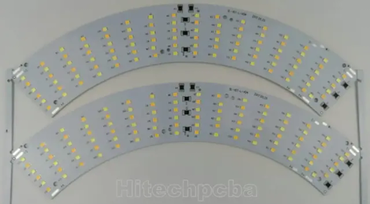
LED PCB Assembly
What is the LED Circuit Board assembly?
Generally, LED PCB assembly is considered to be a circuit board that has the LED components soldered to it. The LED is soldered to the printed circuit board and features a chip that creates the light as electrically connected. A thermal heat sink and a ceramic base are used to bond the chip. Not all the PCB products can be used in Led industry, as an LED PCB is easy to create a high volume of heat, but making it hard to cool with traditional methods. For this reason, metal core PCB is widely used in LED application because of their enhanced ability to dissipate heat, especially aluminum pcb is often used to fabricate PCB for LED lights.
We’ve had great LED PCB assembly experiences with top LED chips to brand such as Cree, Luxeon, Osram, Nichia, Lumileds, MLS, EVERLIGHT, Samsung, LG, Seoul., etc. PCB LED lights can be incorporated into numerous lighting applications due to their combination of excellent energy efficiency, low cost and maximum design flexibility.

Application of LED PCB Assembly
Hitechpcba serves customers in different industries, providing highly reliable and innovative LED PCBs for various applications:
• Horticulture light LED PCB Assembly
• LED controller PCB Assembly
• Computer LED display and indicators
• LED lights PCB Assembly for medical use
• Automotive LED PCBs Assembly include PCBs for brake lights and headlights
• Street lighting LED PCB Assembly
• Flashlights and camping accessories
• Traffic light PCB Assembly
• Commercial lighting LED PCB Assembly
LED PCB Assembly specification
Number of layers for LED PCB
These layers are made up of aluminum and magnesium, but now have Copper base material and Ceramic base materials for LED PCB industry, we can meet it.
Aluminum LED PCBs stand out among other PCBs because it has a good insulation characteristic and has a better machinery performance, the cheap cost is one important factor too.
Types of layers for LED PCB Assembly
Normally, the base layer is made using aluminum alloy metal.
This aluminum alloy substrate used in making the base makes it ideal for through-hole technology which transfers and dissipates heat.
A thermal insulation layer is made using some ceramic polymer which has good viscoelasticity characteristics.
It is highly heat resistant and protects the PCB against heat and mechanical stress.
The circuit layer, which is covered by a copper foil which can range from one to ten ounces.
LED Board type- single or in panel
Some boards are shapeless. For this reason, LED PCB panels are used. This reduces time, labor production and testing time.
Some LED PCB Assembly is done on a single board while others are done on panel boards.
LED PCB Assembly Process
Roughly, the PCBA process can be divided into theses phases: soldering paste printing > SMT (surface mounted technology) > reflow soldering > AOI (automated optical inspection)> THT (through-hole technology) > wave soldering > touch-up and cleaning > IC-programming > FCT (functional tests) > aging testing.
Below we show you the process.
Step1. Summarizing Project Information
Before contacting your supplier, make sure you have all the project information. Suppliers will need info following for quoting LED PCB assembly:
Gerber
BOM
LED PCB specification
Quotation quantity
Once you have gathered these information, you can contact us and request for a quote.
Of course, you can also provide the schematic, LED PCB Assembly pictures and even samples to us. The more details they have, the more accurate the supplier’s quotation will be.
Step2. Discussion and details about custom LED PCB Assembly
Different projects will have different requirements. Remember the special requirements mentioned in step 1? That’s going to be the focus of this session. Equipment and engineering capacity will not be identical between suppliers. Make sure your supplier has the equipment to produce and assemble major components and the corresponding testing capabilities.
For example, some vendors don’t have X-ray testing equipment, which means they can’t check the mount quality of BGA chips. Outsourcing this step will increase risk and cost. That’s what you don’t want.
Also, pay attention to time taken by the supplier to quote. Motherboards often contain hundreds or even thousands of components, and they are supplied by different manufacturers. To ensure the quality of the components, the supplier sourcing team will make multi-inquiries from these manufacturers or authorized suppliers to match customer’s requirement, which usually takes 2-3 business days, and even longer for some scarce chips. Therefore, if your project is complex and the supplier quotes you within few hours, double check with them.
Step3. Sample and feedback
After confirming the PI, the supplier will usually provide pre-production samples for your approval. At the same time, the supplier will also confirm with you the logistics plan of the bulk goods. Make sure they understand your shipping requirements, including details on packaging, customs clearance, taxes, etc.
For us to have a successful LED PCB Assembly process, its functions must be defined. Compliance requirement is defined to reduce the effect when components are selected.
The Bill of Materials is then generated from the information installed on the LED PCB.
All this information is used to assemble components which are identified from MOB to the LED PCB.
After that, the routing of traces is determined to each component, based on the size, shape of the circuit board and location of connectors.

Hitech Circuits is trusted by thousands of electronic engineers on their LED PCB assembly projects, from consumer, led bulb to precisely medical LED light, we can help you from the beginning of design stage; From commercial flood LED to industrial high power LED, from automotive LED to military LED, Venture is the perfect place for your LED PCB assembly requirement.
Hitech Circuits has been participated in hundreds and thousands of LED lighting projects, by providing LED PCB and also LED PCB assembly service.
Our LED PCB assembly had covered both ends of the Lighting Class LED size spectrum, assembling some of the largest (2 meter long boards) and some of the smallest LED Lighting applications which used in Medical Endoscopes.
LED PCB Assembly is very crucial in the current industrial development. Many electrical devises are being innovated and the old once being improved.
LED PCBs are useful due to the fact that they are made using materials that can transfer and dissipate heat. This characteristic increases device durability.
The world is changing with new technology, especially PCB technology that plays an essential role in the application of LED circuits. And the LED industry is taking advantage of this technology and growing faster.
As a full feature PCB solutions provider with more than a decade of experience, we're capable to provide LED PCB fabrication, components procurement and LED PCB assembly all under one roof. We can work with you to develop metal core PCB, aluminum circuit boards customized to your specific applications. We feature competitively priced PCBs made with standard FR-4 material that includes a thermal aluminum clad layer that will efficiently dissipate heat, keep all LED PCB components cool and significantly enhance the performance of your products.

LED pcb board, LED pcb assembly
LED with its advantages of high brightness, high efficiency, low heat, long life, is considered the most development potential in the 21st century lighting. In the market and policy driven by the rapid development of the domestic LED industry blowout has formed a relatively complete industrial chain, including the production of epitaxial wafers, chip preparation, packaging, integration, LED application. In 2010, China's LED industry scale, up from $ 827 billion in 2019 to 220 billion yuan, an annual growth rate of over 70%, higher than the 50% level of growth of the global LED lighting industry output value. Among them, the middle and lower reaches of the most complete industrial chain, accounting for 90% of the overall percentage of the GDP.Chinahas become the world's leading LED manufacturing base and important application market.
To further promote the technological innovation of the LED industry, construction and wide application of independent industry chain, China Electronic Appliance Corporation and industry associations to organize the theme of "Focus on the core energy LED Exhibition will be held November 9-11, 2010 in Shanghai International Expo Center and the 78th China Electronics Fair over the same period will be held will create from raw materials, epitaxial wafers, chip, LED bracket, LED accessories, LED packaging and supporting materials, the LED backlight upstream firm to the upstream and downstream enterprises of the display, lighting, landscaping, decorative lighting, traffic lights, automotive lighting, special lighting, to the equipment, instrumentation, software, finance, consulting and other service enterprises and technological exchanges and market trading platform, help the domestic industry sustained and healthy development, and promote the steady expansion of the LED application market.
In the LED industry chain upstream of the epitaxial wafers and LED chips accounted for 70% of the profits of the whole industry, and technology-intensive, capital-intensive, where the core technology of the LED. Well-known epitaxial wafer and chip production enterprises will be exhibited a number of energy-efficient, low heat, cost-effective LED products, many of whom have excellent products of international advanced level.
LED electronic pcb assembly manufacturing 100% Original LED Chip with one-stop in-house pcba services
3 notes
·
View notes
Text

6L High density PCB (HDI PCB)
Board dimensions: 80 x 120mm
Finished board thickness: 1.0mm
Material: FR-4 Tg170
Minimum holes size: 0.1mm
Minimum line width/clearance: 2/3mil
Copper thickness: 2 oz
Solder mask: top and bottom (color: Blue)
Silkscreen: top (color: white)
Finish: immersion gold (top and bottom)
Board stack up: 1 + 4 + 1
If you have HDI PCB manufacturing needs,please feel free to contact [email protected]. Or you can visit our website https://hitechcircuits.com/pcb-products/high-density-interconnect-pcb/ for more information.
0 notes
Text

Introduction to the difference between HDI board and ordinary PCB
HDI board (High Density Interconnector), that is, high-density interconnect board, is a circuit board with a relatively high line distribution density using micro-blind buried hole technology. HDI board has inner and outer layers, and then uses drilling, in-hole metallization and other processes to connect the internal layers of each layer.
HDI board is generally manufactured by lamination. The more times of lamination, the higher the technical level of the board. Ordinary HDI board is basically 1-time lamination, and high-end HDI uses 2 or more times of lamination technology, and also uses advanced PCB technologies such as stacking holes, electroplating filling holes, and laser direct drilling.
When the density of PCB increases to more than eight layers, the cost of manufacturing with HDI will be lower than the traditional complex pressing process. HDI board is conducive to the use of advanced assembly technology, and its electrical performance and signal accuracy are higher than traditional PCB. In addition, HDI boards have better improvements in radio frequency interference, electromagnetic wave interference, electrostatic discharge, heat conduction, etc.
Electronic products are constantly developing towards high density and high precision. The so-called "high" not only improves the performance of the machine, but also reduces the size of the machine. High-density integration (HDI) technology can make the terminal product design more miniaturized while meeting higher standards of electronic performance and efficiency. Currently, many popular electronic products, such as mobile phones, digital (cameras), laptops, automotive electronics, etc., use HDI boards. With the upgrading of electronic products and market demand, the development of HDI boards will be very rapid.
Introduction to ordinary PCB
PCB (Printed Circuit Board), the Chinese name is printed circuit board, also known as printed circuit board, is an important electronic component, a support for electronic components, and a carrier for electrical connections of electronic components. Because it is made using electronic printing technology, it is called a "printed" circuit board.
Its main function is to avoid manual wiring errors due to the consistency of similar printed boards after electronic equipment adopts printed boards, and can realize automatic insertion or mounting, automatic soldering, and automatic detection of electronic components, ensuring the quality of electronic equipment, improving labor productivity, reducing costs, and facilitating maintenance.
HDI board is a high-density interconnection circuit board. The boards that are electroplated with blind holes and then pressed again are all HDI boards, which are divided into first-order, second-order, third-order, fourth-order, and fifth-order HDI. For example, the motherboard of iPhone 6 is a fifth-order HDI.
Simple buried holes are not necessarily HDI.
How to distinguish between first-order, second-order, and third-order HDI PCBs
The first-order is relatively simple, and the process and technology are easy to control.
The second-order is troublesome. One is the alignment problem, and the other is the problem of punching and copper plating. There are many designs for the second order. One is that the positions of each order are staggered. When the adjacent layer needs to be connected, it is connected through wires in the middle layer. The method is equivalent to two first-order HDIs.
The second is that two first-order holes overlap and achieve the second order by superposition. The processing is similar to two first-order holes, but there are many process points that need to be specially controlled, which is what is mentioned above.
The third is to drill directly from the outer layer to the third layer (or N-2 layer). The process is very different from the previous one, and the difficulty of drilling is also greater.
For the third order, the second order is analogous.
Ordinary PCB boards are mainly FR-4, which is made of epoxy resin and electronic grade glass cloth. Generally, traditional HDI uses adhesive copper foil on the outermost surface. Because laser drilling cannot penetrate glass cloth, adhesive copper foil without glass fiber is generally used, but the current high-energy laser drilling machine can already penetrate 1180 glass cloth. In this way, there is no difference from ordinary materials.
Email us Cynthia<[email protected]> if you are interested in PCB and PCBA service.
0 notes
Text
Choosing Viasion for your HDI PCB manufacturing offers several advantages. Viasion specializes in high-quality HDI PCB production, providing expertise in design, fabrication, and assembly. With state-of-the-art facilities and a skilled team, Viasion ensures precision, reliability, and cost-effectiveness for your HDI PCB projects.
0 notes
Text

Substrate-like PCB China
Layer count: 4 layer Material: BT, 0.38 mm, 0.33 OZ for all layer Minimum trace: 30 um Minimum space(gap): 30um Minimum hole: 0.10mm Surface finished: ENEPIG ( Ni 200U" Pd 2U" Au 2U") Panel size: 258*76mm/198up Characteristics: Low CTE, high speed, ENEPIG for bonding, BT raw material
1 note
·
View note
Text
HDI (High Density Interconnect) PCB
HDI (High Density Interconnect) is a high density interconnect technology that enables more tracks and interconnect through holes. Compared to traditional circuit boards, HDI technology can achieve more functions in a smaller size.

0 notes
Text
The Evolution of PCB Manufacturing: From Basics to High-Performance Boards
PCB manufacturing has evolved from single-layer boards to high-performance, multi-layered designs, enabling innovation in automotive, healthcare, telecommunications, and aerospace. Learn how cutting-edge PCB technologies support modern electronics and drive UK industries forward. Explore advanced PCB solutions for your business today.
#PCB manufacturing evolution#high-performance PCBs#multi-layer PCB design#PCB for 5G networks#advanced PCB technology#UK PCB industry#flexible PCBs#PCB signal integrity#automotive PCB solutions#medical device PCBs#aerospace PCB manufacturing#PCB miniaturisation#HDI PCBs#thermal management in PCBs#next-gen PCB solutions#A-Gas Electronic Materials
0 notes
Text
https://www.maximizemarketresearch.com/market-report/global-high-density-interconnect-hdi-pcb-market/30122/
Growing consumer electronics sales, as well as a significant increase in demand for HDI PCBs in these applications, are driving the global HDI PCB market.
0 notes
Text

Letting you focus on design and marketing, we specialize in handling your procurement and manufacturing processes.Submit Your Gerber and BOM Files for a Free Fab/Assembly Quote!
#pcb#pcba#pcblayout#pcbfabrication#pcbdesign#pcbassembly#SMT#DIP#BGA#electronics#component#USB#ledboard#aluminum#pcbboard#IC#power#supply#Bluetooth#HDI#sports#headset
0 notes
Text
Circuit Board, PCB assembly & electronics manufacturing service provider from China (hitechcircuits.com)
What is a prototype PCB assembly?
PCB prototyping is the experimentation pilot stage of the product which is to be mass produced at a later stage. This is more of an experiment which is done after the initial discussions and the design. This offers a pre-production analysis of the boards that are to be manufactured, reducing the possible number of errors in the PCB design. PCB prototypes help the manufacturer analyze the strengths as well as weak areas of their proposed circuit boards. Prototypes also serve as a reference point for future versions of the same product. At Hitechpcba, we handle PCB prototype assembly in quantities from one to hundred printed circuit boards.
We have acquired capabilities that enable us to serve our clients better. All these years, we have worked on many complex prototype PCB assembly projects, and we believe the following capabilities have helped us serve our clients better.
Prototype PCB Assembly Services: We specialize in the following prototype printed circuit board assembly services.
SMT: We can provide single-sided and double-sided surface mount PCB assemblies in different specifications.
Plated Through Hole: We offer plated through hole assembly with selective soldering.
Mixed Assemblies: We often work on projects involving mixed assemblies – through-hole and SMT and electromechanical assemblies.
PCBA Testing: All the PCBA functional testing is performed in-house. Over the years, we have invested in various test fixtures and equipment, which helps us ensure the quality of PCBA. Currently, we provide the following types of PCBA testing services:
Flying probe testing for PCB
Functional testing including system and board-level testing
General PCB Assembly Capabilities: Our general PCB assembly capabilities are not limited to these:
RoHS, leaded or lead free, clean and no chemistries
PCB components including various types of QFNs, BGAs, 0105, 0201, 0804, and press fit components in small quantities.

What are the benefits of a prototype PCB assembly?
Prototype PCB assembly comes with several advantages. These benefits play a major role in the facilitation of your PCB manufacturing. Some of these benefits include:
Detection of Flaws Early
With prototype PCB, you will easily detect whatever flaws are present during the product’s development stages. This will allow you to solve the issues thereby saving you some money if you had gone ahead to make the production having the flaws in them.
If you go ahead to make changes during the production, there may be a need for more technicalities, and this may be expensive.
Testing of Each Component
With a prototype, you will be able to test all your system’s elements individually before you go ahead to set it up. You should do this because it is important especially for very complex projects composed of several parts that are PCB based.
When you validate each of these components, you will be able to identify those areas having issues that you should look into. This is the only way the project can function the right way.
Reduction in Total Costs
Utilizing the prototype bare PCB for any of your projects could go a long way in reducing what you’ll have spent in total for the project. With prototyping, you will be able to notice those errors in your project and then make corrections before you start the real production.
As soon as these flaws have been checked and rectified, then you may continue with the manufacturing of your Printed circuit boards in large quantities, thereby saving you unnecessary costs.
High-Quality PCBs
Why prototyping your PCB is important is to help you test if your project will function effectively. When we talk of testing, it involves the identification of errors present and then rectifying and making corrections to them.
Therefore, the eventual PCB after the prototyping will be of high quality that surely meets standards set internationally.
Less Turnaround Time
With prototype PCB assembly, you will be able to reduce the total time used in producing your printed circuit board. While making use of prototype printed circuit boards, you’ll be able to see the errors and then make corrections before you start the actual production.
Therefore, the eventual prototype will be free of defects. This implies that your PCBs will be produced quickly by your manufacturer.

What are the different types of prototype PCB assembly services you offer?
With years of market presence and experience, we specializes in the following prototype PCB assembly services.
Plated through-hole (PTH): We can provide the through-hole assembly with selective soldering.
Surface mount technology (SMT): We offer single-sided as well as double-sided SMT board assemblies in varied specifications.
Mixed Assemblies: Our experts often work on projects involving both PTH and SMT assemblies.
What are the types of testing Hitechpcba use for prototype PCB assembly?
Automated Optical Inspection (AOI): This is performed before and after the soldering to identify the component placement, presence, and solder quality.
X-ray Testing: In this type of testing, the operator relies on the X-ray images of the PCB to check the solder joints and lead-less components such as Quad Flat Packs and ball grid arrays, which are generally not visible to naked eyes.
In-Circuit Testing (ICT): This method is used to detect manufacturing defects by testing the electrical properties in the SMT Assembly.
These techniques help us ensure the reliability and accuracy of the circuit boards. In addition to this, it ensures a long operational life of equipment, minimal production losses, streamlined processes, and much more.
What are the capabilities Hitechpcba offer for prototype PCB assemblies?
We specialize in offering IPC compliant, and quick turn PCB assemblies. We are very particular about our scheduled deliveries and timelines, and we deliver without compromising the quality. Our PCBA capabilities are not limited to these. Here are some capabilities we offer through prototype PCB assemblies.
RoHS compliance
Stringent testing procedures
Device encapsulation
Full turnkey, partial turnkey, and kitted/consigned services
Assemblies using Surface Mount (SMT), Thru-hole, Mixed Technology (SMT/Thru-hole), Single and double-sided SMT/PTH, Large parts on both sides, BGA on both sides.
Do you perform a component analysis for prototype PCB assemblies?
Yes, we check the quality and performance of components before mounting them on the circuit boards. This is because a malfunctioning component can affect the performance of the entire circuit board assembly and also pose risks.
What is your standard turnaround time for a prototype PCB assembly?
Our turnaround time for standard applications is two weeks. This timeframe varies depending on the complexity of the applications. However, we are committed to offering quick turnaround times without compromising on quality, functionality, and accuracy, which offers our client a competitive advantage and reduced time to market. You can also request any emergency assistance or queries related to any type of PCB assembly. Our experts will assist you in all possible ways.
How is the cost of prototype PCB assembly estimated?
PCBA costing varies based on the different factors, such as PCBA parts, type of materials to be used, order quantity, and much more. We can also offer quotes and customization options once you share the detailed requirement with us.
We focus on quality and customer satisfaction over anything else. This has helped us build a long list of happy and satisfied customers. So, if you wish to partner with a manufacturer of prototype PCB assembly in China, then don’t hesitate to reach us. Our experts will assist you through all the phases of the prototype PCB assembly process. We look forward to making your experience with us better and memorable.
How to choose prototype pcb assembly manufacturer?
Our pcb prototype assembly service includes the sourcing of components. This allows you to concentrate on what you do best: layout design. We have a dedicated sourcing staff that coordinates with multiple suppliers and distributors to purchase electronic parts as per client requirements, and our staff completes these purchasing particulars in a most efficient manner. We have advanced processes for optimal selection of packaging (cut tape, tube, bulk, etc.) to reduce the total cost. Furthermore, we are capable of cross-referencing parts and even locating hard-to-find and obsolete parts. Customers can be rest assured that when Hitech Circuits substitutes components that they are high quality: we only use the electronic component numbers and manufacturers specified in the BOM. We will not modify your original layout design. Part substitutions take place only with your permission.
The final pcb prototype assembly service cost includes assembly labor charges, bare circuit board rates, and part costs. We understand the importance of prompt delivery. The sooner the components are sourced, the sooner we can begin circuit board fabrication. We thoroughly evaluate engineering inquiries and concerns related to the related parts with our clients before commencing circuit board assembly. The average time taken for pcb manufacturing assembly is about two weeks, which can be further reduced if there are no hard-to-locate components or documentation mistakes.
We have specialized experts to deliver fast turnarounds for prototype circuit board assembly with surface-mount (SMT), through-hole (THT) and mixed-technology components.
Anyone interested in electronics and electronic circuit boards needs to understand the various stages of developing and producing a printed circuit board. It can come in handy when you are seeking a top prototype smt assembly provider. The various production stages of printed circuit boards entail design, prototyping (prototype PCB development and rapid prototyping pcb assembly), and PCB high volume production. Different entities will always seek part of the whole production process depending on their electronic circuit board needs.
However, this article seeks to help you understand everything about prototype PCB assembly, a fundamental aspect of the PCB production process.
Rapid prototyping pcb assembly represents a fundamental phase of the printed circuit production process. It is also inferred as PCBA prototype assembly, SMT or surface-mount technology PCB prototype, PCB sample assembly, etc. From these alternative names, the meaning of prototype assembly regarding printed circuit boards becomes apparent. So what is assembly prototype?
PCB prototype assembly service is a fast prototype printed circuit board assembly primarily used to test fresh or new electronic designs. Consequently, it assists with checking and ensuring quality assurance of the PCB. For instance, it verifies that no bug exists in the test PCB, updates the design, and finds bugs. In most instances, prototype assembly of an electronic project will require two or three iterations to ensure everything is perfect.

Why Choose Hitech Circuits PCB Assembly for Your Prototype PCB Assembly Projects?
There are several PCB manufacturers specializing in prototype PCB assembly services. However, Hitech Circuits stands out owing to the following:
1.Strong Supply Chain: Over the years, we have built strong supply chain relationships in the industry, which helps us fulfill the requirements of turnkey prototype assembly services easily.
2.Fastest Turnaround Times: Our engineering expertise coupled with our understanding of industry requirements and a well-equipped facility enables us to assure the fastest turnaround times of 24-48 hours.
3.Reliability: All the printed circuit boards that we produce are IPC compliant, which helps us assure reliability.
4.Competitive Pricing and Quick Quote: Our supply chain relationships enable us to assure competitive prices. The cost of the PCB prototype assembly will be made available within 24-48 hours.
2 notes
·
View notes
Text

The Advantages of Resin Plugging Used for PCB Holes 1. After filling various blind buried holes with resin, it is beneficial for the vacuum reduction of lamination. 2. After resin filling, it can avoid surface depression caused by insufficient filling of laminated adhesive, which is beneficial for fine circuit fabrication and characteristic impedance control. 3. It can effectively utilize three-dimensional space and achieve any inter-layer interconnection through hole stacking technology. 4. By designing patches on holes, higher-density wiring can be achieved. 5. It can eliminate impurities from entering the through-hole or avoid being entangled in corrosive impurities.
0 notes
Text
PCBA Details Display!!!
#pcb#pcba#pcblayout#pcbfabrication#pcbdesign#pcbassembly#SMT#DIP#BGA#electronics#component#USB#ledboard#aluminum#pcbboard#IC#power#supply#Bluetooth#HDI#sports#headset#flex pcb#fpcway#fpcway.com#flexible circuit board#today on tumblr#rigid-flex pcb#flex circuit pcb#flexible pcb board
0 notes
Text
Seeking High-Quality, Cost-Effective High Density PCBs from a Reliable Chinese Supplier?
Look no further than XPCB Limited, your trusted partner for cutting-edge HDI PCB solutions. We offer a comprehensive range of HDI PCB manufacturing services, from prototyping to mass production, catering to diverse industries, including consumer electronics, automotive, medical devices, and telecommunications. Our state-of-the-art facilities, coupled with our team of experienced engineers, ensure the delivery of PCBs that meet the highest international standards. Our commitment to quality, efficiency, and customer satisfaction has earned us a reputation as a leading HDI PCB manufacturer in China.
0 notes
Text
Explore the characteristics, applications, structure, and manufacturing process of HDI PCBs. Learn how HDI technology is revolutionizing PCB design at Viasion. To achieve this, micro vias, blind and buried vias, and very small trace width/spacing are created and done on printed circuit boards.
0 notes
Text
The Silent Enabler: How IC Substrates Power the Semiconductor Revolution
Breaking Down the IC Substrate Ecosystem
The global IC substrate market has transformed into a $14.6 billion industry (Yole Développement 2025), driven by three core technology segments:

Advanced Packaging Platforms
2.5D/3D IC substrates now enable 12-layer interposers with <1μm alignment precision
Fan-out wafer-level packaging (FOWLP) achieves 0.8μm line/space resolution
Heterogeneous integration substrates support 10+ chiplet configurations
Material Science Breakthroughs
Low-loss dielectrics (Dk<3.0 @ 100GHz) from 8 major chemical suppliers
Nanocomposite thermal interface materials with 15W/mK conductivity
Photosensitive dielectric films enabling 2μm laser patterning
Cutting-Edge Manufacturing Innovations
Leading manufacturers have deployed:
AI-Optimized Production
Neural networks reducing warpage by 40% through real-time parameter adjustment
Digital twin systems predicting yield with 98.7% accuracy
Automated optical inspection achieving 50 defects per billion opportunities
Sustainable Manufacturing
Closed-loop chemical recycling recovering 92% of process materials
Plasma treatment replacing chemical desmear in 35% of facilities
Waterless cleaning systems reducing H2O usage by 8,000 tons/month per fab
Transformative Applications
AI/ML Hardware
NVIDIA's Blackwell GPU platform uses IC substrates with:
8μm microbump pitch
16-layer build-up structure
3D through-silicon via (TSV) integration
Automotive Electronics
Tesla's Dojo 2 training system incorporates:
45μm coreless substrates
Embedded decoupling capacitors
10μm ultra-fine line circuitry
Emerging Technology Frontiers
Quantum Computing
Cryogenic substrates operating at 4K with:
Superconducting niobium interconnects
Quantum-limited loss dielectrics
Magnetic field shielding layers
Biomedical Interfaces
Neural implant substrates featuring:
500nm flexible polyimide circuits
Biocompatible gold metallization
10-year in-vivo stability
Frequently Asked Questions
Why are IC substrates crucial for chiplet designs?
They provide:
Known-good-die (KGD) testing infrastructure
Ultra-short inter-chiplet links (<100μm)
Thermal stress buffering between heterogeneous dies
How do IC substrates enable 6G communications?
Through:
Terahertz waveguides with 0.001dB/mm loss
Antenna-in-package integration
3D electromagnetic shielding structures
What's the roadmap for IC substrate technology?
Key milestones include:
2026: 1μm line/space volume production
2028: Photonic interposer commercialization
2030: Molecular-scale self-assembling substrates
1 note
·
View note
Text

10 layers high density interconnect PCB board made of FR-4, Tg 150 with immersion gold surface treatment.
High-Density Interconnect (HDI) PCB is simply a PCB with more number of interconnections and buried hole, blind hole, occupying minimal space. This results in the miniaturization of the circuit board. The components are placed closer and the board space is significantly reduced but the functionality isn’t compromised. [email protected]
4 notes
·
View notes