#PCB cad
Explore tagged Tumblr posts
Visit Tumblr Blog
Explore Tumblr blogs with no restrictions, modern design and the best experience.
Last Seen Tumblr Blogs


Fun Fact
Tumblr’s website traffic is steadily declining.
Text
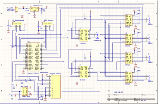
Today (Friday 3rd May 2024) I finally got the schematic of the matrix board plus a few improvements drawn out in the PCB CAD system ready for the next stage of laying out the board. I will probably ponder over this for a few weeks just in case I want to change or improve something else. Two of the signal lines on the attachment connector have been changed to include the I2C channel, as I feel that this could be a very useful communications link for any future attachments that we might need to provide for the robot. Also the DRV8825 driver modules provide a 'Fault' output pin that the previous drivers didn't have. So these four lines have been connected to the Pi for monitoring by the software. The two CD4094 shift register latches are loaded using the Pi's SPI interface and then all sixteen bits are latch simultaneously by a single line from the Pi. It is the most effective way to add lots of synchronised digital output lines to the Pi.
1 note
·
View note
Text
1 note
·
View note
Text
People who draw PCB design for a living have such overinflated egos and sense of importance. Before CAD actual engineers used to do your job with a marker pen or some shit as a totally incidental part of their much more challenging jobs. Get some perspective.
2 notes
·
View notes
Note
do you have any tips & tricks for how to put vector art on a PCB? any specific tools you use? i ended up having to do a crazy complex mix of KiCAD and EasyEDA and Inkscape with various hacky plugins/extensions, i wish there was something easier to get artwork on PCBs.
for EagleCAD we have a python script that can insert any PNG/BMP as well as any vector font by rasterizing it into the silkscreen layers
https://learn.adafruit.com/adafruit-pinguin-for-eagle-cad
https://github.com/adafruit/Adafruit_Pinguin
however! we’re going to see what we can for a KiCAD guide, we’ll post up on tumblr too!
(and there is also this guide!)
22 notes
·
View notes
Text
my custom keeb + sounds:
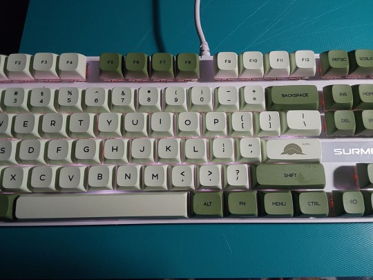
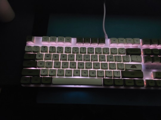

more info below, if u wanna see what i did
its around 65 CAD dollars on amazon, but i got it for 15 using a giftcard my old teacher gave me (i cleaned my highschools fish tanks for 3 years, wasnt expecting any payment but she gave me some money seeing as i would work 1-3 hours daily, sometimes all 5 days of the school week to keep those fish from dying, its a long story eurrr).
it came with the matcha keycaps + some extra keycaps for customization, rgb backlights, and some generic red linear switches (felt like 55g springs) which i later switched out for aliexpress fake holy pandas (67g springs), which are considered one of the best tactile switches out there, and the fake ones are honestly pretty close to the real ones. The stock red linears were good, especially for a starter enthusiast i think, but they were barely lubed and the springs inside were so LOUD. i thought the case was empty because of how loud the spring ping was LOL. to fix it, just l.ube the springs well.
they came factory lu.bed but i still went over them with my own aliexpress (again. i did not want to spend a lot of money) l.ube. they have crazy thock and when over-lub.ed, become creamy.
i did the foam mod using thick felt foam (also from ali.... it was precut to fit perfectly okay) plus another layer of that thin white packaging foam from the keyboard box. Unfortunately, the keyboard, despite saying it can be customized in its description, had the plate and the back case welded :/// i had to cut around the foam to slip it through the welded parts.
i added the thin white foam and some painters tape to the inside of the spacebar keycap to create more thock, which worked very well.
the new ali switches also didnt fit in the front plate?? they fit in the pcb just fine, but the front plate was a little too small or something so when i would push the switches in, theyd fly out. i had to put the thing on the floor and step on it to get some of the keys to stay. i eventually had to frankenstein the original red linear switch cases with the internals of the pandas to get the spacebar and enter keys to sit right and fit with the stabilizers.
the stabilizers are white plastic and removable, as long as you unsrew the entire top part of the case first LOL. they work fine with the stock switches, but struggle to move the keys up or down without sticking if you use any other switch.
the fekker holy pandas worked well, especially since they were fakes and a lot cheaper than the real ones - real pandas cost about 83 CAD for 70 pcs, while i got 110 for 25 CAD! there were a few in the bag that didnt work, and they were shipped in a plain plastic bag, but they give you extras so you have enough working ones for a full size keyboard (which has 104 keys).
i accidentally damaged the pcb copper wiring stuff by pushing in a switch without checking if the pins were aligned; the pins bent instead of going into the holes and scratched the wires. because of this, i lost function in both the f11 function key and the print screen key. i dont ever use those so im fine with it.
long post over. i love her so much
3 notes
·
View notes
Text
Comprehensive Guide to PCB Board Design & Printed Circuit Assembly for Optimal Electronic Performanc
Compre
Modern electronics rely heavily on printed circuit boards (PCBs). Without well-designed PCBs and quality assembly, devices can become unreliable or fail prematurely. Whether you’re a designer or manufacturer, understanding how to create and assemble high-quality PCBs is crucial. This guide covers essential design principles, manufacturing methods, testing, and tips for better PCB performance.
Understanding PCB Board Design Fundamentals
The Role of PCB Design in Electronics Functionality
PCB design is the blueprint that shapes how your device works. It directly influences electrical signals, heat management, and overall durability. Poor design can lead to issues like signal interference or overheating, hurting the product's performance. Good design results in a more reliable, longer-lasting device that customers can count on.
Essential Components of a PCB Design
A PCB isn’t just a green board with some wires. It includes multiple elements such as:
Layers: These are the different sheets of the PCB, repeating signals or power.
Traces: Thin lines of copper that connect components.
Pads: Contact points for mounting parts like chips or resistors.
Vias: Small holes that link traces on different layers.
Components: Resistors, capacitors, ICs, and other parts attached to the board.
Each piece affects how well the circuit functions. Proper layout and placement ensure electrical signals flow smoothly and the device functions as intended.
Designing for Manufacturing (DFM) Best Practices
Designing with manufacturing in mind helps lower costs and speeds up production. Here are key tips:
Use standard component sizes and footprints.
Keep traces wide enough to handle current.
Avoid tiny vias or complex shapes that are hard to manufacture.
Place components logically to reduce assembly time.
Minimize the number of layers if possible. Fewer layers often mean lower costs.
These practices make it easier for factories to produce your design without errors or delays.
Types of Printed Circuit Boards and Their Applications
Rigid PCBs
Rigid PCBs are the most common type. They’re made of solid material, like fiberglass, that keeps the board stiff. You’ll find these in everything from computers to appliances. They’re reliable, cost-effective, and easy to handle during assembly.
Flexible and Rigid-Flex PCBs
Flexible PCBs bend and fold, fitting into small spaces inside devices. Rigid-flex combines both types, offering stiffness where needed and flexibility elsewhere. These are popular in wearable tech and smartphones, where space is tight.
High-Frequency and HDI PCBs
Special boards designed for fast signals — known as high-frequency PCBs — are used in radio, radar, and satellite systems. HDI (High-Density Interconnect) PCBs pack more components into less space, ideal for miniaturized electronics like medical devices or smartphones.
The Printed Circuit Assembly (PCA) Process
From Design to Production: Step-by-Step Overview
A typical PCA process includes:
Designing the circuit using CAD tools.
Verifying the design for errors.
Creating prototypes for testing.
Moving into full-scale manufacturing.
Assembling components via soldering.
At every step, quality checks are essential to prevent costly mistakes later.
Key Manufacturing Techniques
Surface-Mount Technology (SMT): Attaching components on the surface. It’s fast and suitable for high-volume production.
Through-Hole Assembly: Inserting pins into drilled holes. Best for parts needing full mechanical strength.
Automated Assembly: Robots place components quickly with high precision.
Manual Assembly: Used for small runs or complex parts, but slower.
Choosing the right method impacts the speed and quality of your PCB production.
Quality Control and Inspection
Regular inspections catch problems early:
X-ray Inspection: Checks hidden solder joints.
Automated Optical Inspection (AOI): Finds defects on the surface.
SPI (Solder Paste Inspection): Ensures correct solder paste volume.
Complying with standards like IPC-610 and IPC-2221 helps keep quality high and consistent.
Critical Factors Influencing PCB and PCA Quality
Material Selection for Durability and Performance
Choosing the right materials makes a difference:
Substrates like FR-4 are common but vary in quality.
Copper thickness affects current capacity.
Solder masks prevent shorts and corrosion.
Durable materials stand up to temperature, vibration, and environmental stress.
Design for Reliability
To keep your device working long-term:
Minimize electrical interference by proper grounding.
Manage heat by placing heat-sensitive parts away from heat sources.
Use clear labels and ample space for easy assembly and maintenance.
Good practice prevents failure and reduces warranty repairs.
Environmental Considerations
PCBs face many conditions:
Use conformal coatings to protect from moisture.
Choose vibration-resistant designs for mobile devices.
Select temperature-tolerant materials for harsh environments.
Designing for these factors enhances lifespan and performance.
Cost Optimization
Balancing quality with budget is key:
Use standard components rather than custom parts.
Avoid overly complex designs.
Optimize layout for easy assembly.
Good planning reduces waste and keeps costs in check.
Best Practices for PCB Design and Assembly Optimization
Design Tips for Ease of Assembly
Properly space components for automatic placement.
Use clear silkscreen labels to identify parts.
Keep copper traces away from component pads for easier soldering.
Simplicity saves time during manufacturing and reduces errors.
Enhancing Manufacturing Efficiency
Stick to standard footprints.
Avoid intricate shapes on copper traces.
Use consistent pad sizes and pad-to-component spacing.
This approach speeds up production and keeps quality high.
Post-Assembly Testing and Validation
Once assembled, testing is crucial:
Conduct functional testing to verify operation.
Use burn-in tests to detect early failures.
Carry out long-term stress tests for durability.
Thorough testing ensures your product withstands real-world use.
Collaborating with Proven PCB Manufacturers
Choose manufacturers with:
Certifications like IPC-6012 or ISO 9001.
Experience in your specific PCB type.
Good communication and ability to meet deadlines.
Partnering with reliable suppliers reduces risks and improves final product quality.
Case Studies and Real-World Examples
Some companies have achieved great results by focusing on PCB design. For example, an electronics firm reduced their device failure rate by improving trace routing and component placement. Conversely, poor design choices, such as crowded traces, led to short circuits and costly recalls. Learning from these stories highlights the importance of meticulous planning and quality control.
Conclusion
Creating a high-performance PCB, from design to assembly, is essential for reliable electronics. Focus on good design practices, choose the right materials, and work with experienced manufacturers. Regular testing and inspection help catch issues before products hit the market. As technology advances, keep an eye on trends like miniaturization and high-frequency PCBs. Staying current ensures your designs remain competitive and durable. Quality now means better devices, happier users, and fewer headaches later.
0 notes
Text
Revolutionizing Manufacturing: The Ultimate All-in-One Autodesk Fusion 360 Platform
Unlocking Innovation: How Fusion 360 Is Shaping the Future of Manufacturing
In today's rapidly evolving technological landscape, the way we design and manufacture products is undergoing a revolutionary transformation. Autodesk Fusion 360 stands at the forefront of this change, offering an all-in-one platform that seamlessly integrates CAD, CAM, CAE, and PCB software into a unified environment. This groundbreaking approach not only streamlines the development process but also democratizes access to advanced manufacturing tools, empowering both hobbyists and professionals to bring their ideas to life with unprecedented ease and efficiency.
Fusion 360's cloud-based architecture means that design collaboration is now more accessible than ever. Teams from around the world can work together in real-time, sharing ideas, making modifications, and resolving issues instantly. This collaborative capability accelerates innovation, reduces time-to-market, and fosters a more inclusive approach to product development. Whether you're a startup entrepreneur or a seasoned engineer, Fusion 360 provides the flexibility to adapt to your unique needs and project scope.
One of the platform's standout features is its integrated CAD, CAM, and CAE functionalities, which eliminate the need for multiple software solutions. Users can design complex geometries, simulate real-world conditions, and generate manufacturing-ready files all within a single environment. This integration significantly reduces errors, saves costs, and shortens production cycles, making it a game-changer for manufacturing workflows.
Moreover, Fusion 360's support for PCB design broadens its application scope, allowing electrical engineers to develop and test circuit boards alongside mechanical components. This holistic approach ensures that all aspects of a product are considered early in the development process, resulting in more innovative and reliable end products.
The platform is also highly accessible, offering an affordable pricing model that makes advanced manufacturing tools available to a broader audience. Whether you're a hobbyist working on your latest project or a professional designing complex industrial equipment, Fusion 360 provides the tools and support needed to turn ideas into reality.
Looking ahead, the future of making things is undoubtedly linked to platforms like Fusion 360 that foster collaboration, integrate multiple disciplines, and leverage cloud technology. As manufacturing becomes more digital and connected, the ability to iterate quickly, share insights, and adapt designs in real-time will be crucial. Fusion 360 exemplifies this future by offering a comprehensive solution that bridges the gap between creativity and production.
To explore how Fusion 360 can revolutionize your product development process, consider buy autodesk fusion 360 license today and join the next generation of innovators shaping the future of manufacturing.
0 notes
Text
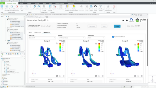
PTC Creo 12: New Tools for Smarter, Faster 3D Design
Discover what’s new in PTC Creo 12 — enhanced simulation, AI-driven design, MBD, and manufacturing tools. Upgrade now with ANH, the trusted PTC Creo reseller in the Delhi NCR region.
Top New Features in Creo 12
1. AI-Driven Design Guidance
Creo 12 takes intelligent design to the next level with built-in AI tools that offer real-time suggestions and improvements.
Get feedback during modeling
Reduce trial-and-error
Improve efficiency with every click
2. Enhanced Model-Based Definition (MBD)
Creo 12 makes MBD more practical and powerful, eliminating the need for traditional 2D drawings.
Improved PMI (Product Manufacturing Information)
Better GD&T annotation support
Clearer data for downstream users

3. Performance & Usability Upgrades
PTC has improved the overall speed, responsiveness, and ease of use:
Faster model regeneration
Smart mini toolbars
Enhanced model tree filters
Customizable dashboards for quick access

4. Creo Simulation Live — More Powerful Than Ever
Simulation Live has been expanded to cover:
Structural & thermal simulations
Better support for nonlinear materials
Real-time design feedback

5. Advanced Multi-Body Design
Creo 12 makes it easier to work with complex parts and assemblies:
Better control over multiple bodies in a single part
New body operations and organization tools
Improved part-to-part interactions
It’s ideal for high-detail engineering and intricate product development.
6. Additive and Subtractive Manufacturing Enhancements
Manufacturing has never been smoother in Creo:
More control over lattice structures
Enhanced 5-axis CAM functionality
New machine support and output formats
Whether you’re 3D printing or using CNC, Creo 12 has you covered.
7. Improved ECAD–MCAD Collaboration
With electronics becoming a bigger part of mechanical products, Creo 12 improves:
PCB visualization
Layer management
Synchronization between electrical and mechanical teams
This helps avoid costly errors during development.
Why Creo 12 is a Must-Have Upgrade
PTC Creo 12 isn’t just for big enterprises — it’s built for everyone who values smart, high-quality design. Whether you’re a design engineer, manager, or product innovator, Creo 12:
Saves time
Reduces errors
Encourages innovation
Supports industry 4.0 goals
Get Creo 12 from Delhi NCR’s Trusted PTC Reseller — ANH
Looking to upgrade your CAD tools or switch to Creo 12? ANH is a leading authorized PTC reseller in the Delhi NCR region. From licensing to training, we help businesses unlock the full potential of Creo.
Contact ANH today to get started with Creo 12!
✅ Conclusion: Welcome to the Future of Design
PTC Creo 12 is more than just an upgrade — it’s a gateway to smarter design, quicker development, and stronger innovation. With new AI tools, advanced simulations, and seamless usability, it’s built to give your team a competitive edge.
Design faster. Design smarter with Creo 12.
0 notes
Text
Mechatronic Design Engineer: Bridging Mechanical, Electrical, and Software Engineering
The role of a Mechatronic Design Engineer is at the cutting edge of modern engineering. Combining the principles of mechanical engineering, electronics, computer science, and control systems, mechatronic engineers design and develop smart systems and innovative machines that improve the functionality, efficiency, and intelligence of products and industrial processes. From robotics and automation systems to smart consumer devices and vehicles, mechatronic design engineers are the architects behind today’s and tomorrow’s intelligent technology.
What Is Mechatronic Engineering?
Mechatronics is a multidisciplinary field that integrates various engineering disciplines to design and create intelligent systems and products. A mechatronic system typically consists of mechanical components (such as gears and actuators), electronic systems (sensors, controllers), and software (embedded systems and algorithms).
In practical terms, a Mechatronic Design Engineer might work on:
Industrial robots for factory automation.
Autonomous vehicles.
Consumer electronics (like smart appliances).
Medical devices (robotic surgery tools, prosthetics).
Aerospace systems.
Agricultural automation equipment.
These professionals play a vital role in building machines that can sense, process, and respond to their environment through advanced control systems.
Core Responsibilities of a Mechatronic Design Engineer
Mechatronic design engineers wear multiple hats. Their responsibilities span the design, simulation, testing, and integration of various components into a unified system. Key responsibilities include:
Conceptual Design:
Collaborating with cross-functional teams to define product requirements.
Designing mechanical, electrical, and software systems.
Creating prototypes and evaluating design feasibility.
Mechanical Engineering:
Designing moving parts, enclosures, and structures using CAD tools.
Selecting materials and designing components for performance, durability, and manufacturability.
Electrical Engineering:
Designing circuit boards, selecting sensors, and integrating microcontrollers.
Managing power systems and signal processing components.
Embedded Systems and Software Development:
Writing control algorithms and firmware to operate machines.
Programming in languages like C, C++, or Python.
Testing and debugging embedded software.
System Integration and Testing:
Bringing together mechanical, electrical, and software components into a functional prototype.
Running simulations and real-world tests to validate performance.
Iterating design based on test data.
Project Management and Documentation:
Coordinating with suppliers, clients, and team members.
Preparing technical documentation and user manuals.
Ensuring compliance with safety and industry standards.
Skills Required for a Mechatronic Design Engineer
Being successful in mechatronic engineering requires a broad skill set across multiple disciplines:
Mechanical Design – Proficiency in CAD software like SolidWorks, AutoCAD, or CATIA.
Electronics – Understanding of circuits, PCB design, microcontrollers (e.g., Arduino, STM32), and sensors.
Programming – Skills in C/C++, Python, MATLAB/Simulink, and embedded software development.
Control Systems – Knowledge of PID controllers, motion control, automation, and feedback systems.
Problem Solving – Ability to approach complex engineering problems with innovative solutions.
Collaboration – Strong communication and teamwork skills are essential in multidisciplinary environments.
Industries Hiring Mechatronic Design Engineers
Mechatronic engineers are in demand across a wide array of industries, including:
Automotive: Designing autonomous and electric vehicle systems.
Robotics: Creating robotic arms, drones, and autonomous platforms.
Manufacturing: Developing automated assembly lines and CNC systems.
Medical Devices: Designing wearable health tech and robotic surgery tools.
Aerospace: Building UAVs and advanced flight control systems.
Consumer Electronics: Creating smart appliances and personal tech devices.
Agriculture: Developing automated tractors, irrigation systems, and crop-monitoring drones.
Mechatronics in the Age of Industry 4.0
With the rise of Industry 4.0, smart factories, and the Internet of Things (IoT), the demand for mechatronic design engineers is rapidly increasing. These professionals are at the forefront of integrating cyber-physical systems, enabling machines to communicate, adapt, and optimize operations in real-time.
Technologies such as AI, machine learning, digital twins, and cloud-based monitoring are further expanding the scope of mechatronic systems, making the role of mechatronic engineers more strategic and valuable in innovation-driven industries.
Career Path and Growth
Entry-level mechatronic engineers typically begin in design or testing roles, working under experienced engineers. With experience, they may move into project leadership, system architecture, or R&D roles. Others transition into product management or specialize in emerging technologies like AI in robotics.
Engineers can further enhance their careers by obtaining certifications in areas like:
PLC Programming
Robotics System Design
Embedded Systems Development
Project Management (PMP or Agile)
Advanced degrees (MS or PhD) in mechatronics, robotics, or automation can open opportunities in academic research or senior technical roles.
Future Trends in Mechatronic Design Engineering
Human-Robot Collaboration: Cobots (collaborative robots) are transforming how humans and robots work together on factory floors.
AI and Machine Learning: Enabling predictive maintenance, adaptive control, and smarter decision-making.
Wireless Communication: Integration with 5G and IoT platforms is making mechatronic systems more connected.
Miniaturization: Smaller, more powerful components are making devices more compact and energy-efficient.
Sustainability: Engineers are designing systems with energy efficiency, recyclability, and sustainability in mind.
Conclusion
A Mechatronic Design Engineer by Servotechinc plays a pivotal role in shaping the future of intelligent machines and systems. As industries become more automated and interconnected, the demand for multidisciplinary expertise continues to rise. Mechatronic engineering offers a dynamic and rewarding career path filled with opportunities for innovation, creativity, and impactful problem-solving. Whether you’re designing a robot that assembles products, a drone that surveys farmland, or a wearable medical device that saves lives—mechatronic design engineers are truly the bridge between imagination and reality in the world of modern engineering.
0 notes
Text
CNC Laser Cutting Machine: Precision, Power, and Productivity in Modern Fabrication
In today's manufacturing landscape, precision and efficiency are critical to staying competitive. One of the most transformative technologies in modern metalworking and fabrication is the CNC Laser Cutting Machine. This advanced equipment blends the accuracy of laser technology with the automation of computer numerical control (CNC), offering unmatched results across various industries.
Whether you're cutting thin sheet metal or intricate designs, a CNC laser cutting machine offers the speed, accuracy, and versatility needed in a fast-paced industrial environment.
What is a CNC Laser Cutting Machine?
A CNC Laser Cutting Machine is a high-precision tool used to cut and engrave materials by directing a focused laser beam through CNC programming. The term CNC (Computer Numerical Control) refers to the system that guides the laser head based on a digital design or CAD file.
This machine can cut through various materials, including:
Metals (steel, stainless steel, aluminum, copper)
Plastics
Wood
Acrylic
Fabrics and composites
The key feature of a CNC laser cutter is its ability to perform complex, high-detail cuts with exceptional consistency and minimal material waste.
How It Works
Design Input: A part or product is designed in CAD (Computer-Aided Design) software.
Conversion to CNC Code: The design is translated into G-code or another CNC-compatible format.
Material Placement: The material is loaded onto the machine's cutting bed.
Laser Activation: The machine directs a high-powered laser beam through lenses or fiber optics.
Precision Cutting: The CNC system moves the laser head to follow the programmed path, cutting or engraving the material with pinpoint accuracy.
Types of CNC Laser Cutting Machines
1. CO₂ Laser Cutting Machines
Ideal for non-metal materials (wood, plastics, glass, textiles)
Common in signage, furniture, and packaging industries
2. Fiber Laser Cutting Machines
Optimized for metals (steel, aluminum, brass, etc.)
Faster, more energy-efficient, and lower maintenance than CO₂ systems
3. Nd:YAG Laser Cutting Machines
Suitable for both metal and non-metal applications
Often used where high peak power and pulsing are needed
Key Benefits of CNC Laser Cutting Machines
✅ High Precision
Laser cutting offers exceptionally tight tolerances, ideal for complex and detailed cuts with minimal deviation.
✅ Speed and Efficiency
Faster cutting speeds compared to traditional methods reduce production time, particularly for thin to medium-thickness materials.
✅ Automation and Repeatability
CNC programming ensures each cut is exactly the same, making it perfect for batch production.
✅ Minimal Waste
The precision of laser cutting minimizes material wastage and reduces the need for rework.
✅ Versatility
Cuts a wide variety of materials and thicknesses without changing tools.
✅ Clean Cuts with Smooth Edges
Reduces or eliminates the need for secondary finishing processes like deburring or grinding.
Applications Across Industries
Automotive: Cutting structural and aesthetic components
Aerospace: Producing lightweight, high-precision parts
Architecture: Laser-cut panels and decorative designs
Signage and Advertising: Acrylic signs, logos, and lettering
Electronics: PCB fabrication and enclosure cutting
Medical Devices: Precise and sterile cutting of small, complex parts
Considerations When Choosing a CNC Laser Cutting Machine
Before investing, consider:
Laser power (watts) depending on material type and thickness
Working area size for the size of parts you'll be cutting
Software compatibility for CAD/CAM systems
Maintenance requirements and after-sales service
Material versatility and future expansion needs
Final Thoughts
The CNC Laser Cutting Machine is more than just a cutting tool—it's a powerful solution for modern manufacturing challenges. It provides the perfect blend of automation, accuracy, and speed, enabling manufacturers to produce higher quality parts with lower costs and faster turnaround times.
As industries continue to innovate, integrating CNC laser cutting technology into your operations can provide a strong competitive edge.
0 notes
Text
Global Polyurethane Foam Mattress Market Forecast (2025–2031): Growth, Trends & Strategic Insights
"
The Global Polyurethane Foam Mattress Market is projected to grow steadily from 2025 through 2031. This report offers critical insights into market dynamics, regional trends, competitive strategies, and upcoming opportunities. It's designed to guide companies, investors, and industry stakeholders in making smart, strategic decisions based on data and trend analysis.
Report Highlights:
Breakthroughs in Polyurethane Foam Mattress product innovation
The role of synthetic sourcing in transforming production models
Emphasis on cost-reduction techniques and new product applications
Market Developments:
Advancing R&D and new product pipelines in the Polyurethane Foam Mattress sector
Transition toward synthetic material use across production lines
Success stories from top players adopting cost-effective manufacturing
Featured Companies:
Tempur Sealy International
Serta Simmons Bedding
Sinomax
Sleemon
Recticel
Corsicana
MLILY
Sleep Number
Hilding Anders
Ashley
Pikolin
Derucci
King Koil
Get detailed profiles of major industry players, including their growth strategies, product updates, and competitive positioning. This section helps you stay informed on key market leaders and their direction.
Download the Full Report Today https://marketsglob.com/report/polyurethane-foam-mattress-market/1007/
Coverage by Segment:
Product Types Covered:
King Size
Queen Size
Single Size
Applications Covered:
Private Households
Hotels
Hospitals
Others
Sales Channels Covered:
Direct Channel
Distribution Channel
Regional Breakdown:
North America (United States, Canada, Mexico)
Europe (Germany, United Kingdom, France, Italy, Russia, Spain, Benelux, Poland, Austria, Portugal, Rest of Europe)
Asia-Pacific (China, Japan, Korea, India, Southeast Asia, Australia, Taiwan, Rest of Asia Pacific)
South America (Brazil, Argentina, Colombia, Chile, Peru, Venezuela, Rest of South America)
Middle East & Africa (UAE, Saudi Arabia, South Africa, Egypt, Nigeria, Rest of Middle East & Africa)
Key Insights:
Forecasts for market size, CAGR, and share through 2031
Analysis of growth potential in emerging and developed regions
Demand trends for generic vs. premium product offerings
Pricing models, company revenues, and financial outlook
Licensing deals, co-development initiatives, and strategic partnerships
This Global Polyurethane Foam Mattress Market report is a complete guide to understanding where the industry stands and how it's expected to evolve. Whether you're launching a new product or expanding into new regions, this report will support your planning with actionable insights.
" Exclusion Chromatography (SEC) HPLC Columns Cell-Site Simulators Ship Dismantling CAD/CAM Software for Sheet Metal Ship Management and Crew Management Rebar Coupler Modular Office Furniture Consumer Goods (CPG)ing Software and Platforms Energy-as-a-Service (EaaS) Glass-Melting Furnaces Vacuum Plasma Machine for Bare PCB Manufacturing Direct to Garment Printers Under Eye Gel
0 notes
Text
What Sets Apart a Great Electronics Design Engineer and a Top-Tier PCB Designer
Developing cutting-edge products requires more than just a basic understanding of electronics—it demands specialized expertise at multiple levels of the design process. While the roles of an electronics design engineer and a PCB designer often overlap, each discipline has its own set of core skills, priorities, and best practices. Understanding these differences can help companies build stronger teams and ensure both functionality and manufacturability from concept to production.
1: Foundations: Concept vs. Layout
Electronics Design Engineer
System-level thinking: Architects circuits that meet performance, power, and cost targets.
Component selection: An electronics design engineer chooses processors, sensors, power supplies, and other parts based on specifications and availability.
Simulation and validation: Uses SPICE, MATLAB, or custom scripts to verify that circuits behave as intended under various conditions.
PCB Designer
Physical realization: Translates schematic diagrams into board layouts, deciding component placement, routing, and layer stacks.
Signal integrity: Manages trace lengths, impedance control, and differential pairs to prevent timing mismatches and noise.
Thermal management: Integrates heat sinks, copper pours, and thermal vias to maintain reliable operating temperatures.

2: Technical Skills: Breadth vs. Depth
Breadth of Knowledge (Engineer)
A great electronics engineer understands analog and digital domains, power management, RF techniques, and often systems integration. Their toolkit includes:
Circuit simulation tools (e.g., Cadence, LTspice)
Firmware debugging (e.g., JTAG, SWD)
Test equipment (oscilloscopes, spectrum analyzers)
Depth of Expertise (PCB Designer)
A top-tier PCB designer goes deep into board stack-up design, advanced routing strategies, and material characteristics:
PCB CAD software mastery (e.g., Altium Designer, Mentor Xpedition)
High-speed design considerations (e.g., controlled impedance, crosstalk analysis)
3: Collaboration and Workflow
Communication Styles
Electronics engineers often work in cross-functional teams—mechanical, software, and compliance—to validate overall design requirements. Their deliverables include schematics, block diagrams, and simulation reports.
PCB designers interact heavily with manufacturing partners. They must document fabrication drawings, assembly notes, and BOM details clearly to avoid production delays.
By recognizing the strengths each role brings—and fostering close collaboration between them—teams can bring innovative, reliable products to market faster and more efficiently.
Source: https://extrondesignservice.blogspot.com/2025/05/what-sets-apart-great-electronics.html
0 notes
Text
Top Quality Control Methods in PCB Manufacturing

Top Quality Control Methods in PCB Manufacturing You Should Know
Circuit boards form the backbone of most modern electronic devices. PCBs must meet the highest quality standards as they are used across various industries, including consumer, medical, and automotive electronics, ensuring reliability and performance. Quality control (QC) in PCB fabrication should be perceived as a compulsory necessity and not just a best practice. Let’s discuss the key aspects of quality control in circuit board manufacturing, including its significance, methods, and benefits.
Why Quality Control is Crucial in PCB Fabrication?
Even the most minor defects in circuit boards may usually lead to a malfunction. It requires strict testing and inspection for flawless production. PCB quality control is important for the following reasons:
1. Reliability of Product
Circuit boards must work perfectly to ensure device reliability. Even microscopic imperfections may cause malfunctioning, data loss, or total system blackout. Such severe results are important in high-value medical equipment or aerospace systems. Implementing quality control actions during the manufacturing process allows for the early detection and elimination of defects.
2. No Delays and Reduces Costs
It is easier to address and solve problems during production than to deal with failures after manufacturing. If quality control is absent, defective boards will need reworking or replacement, which adds costs and delays to the production schedule. Powerful QC processes will help minimize these risks and the manufacturers can save time and resources.
3. Customer Satisfaction
High-quality circuit boards transform into highly reliable end products that build customer confidence and satisfaction. Brand loyalty is built by customers receiving devices that are perfect in performance. Quality control ensures that manufacturers deliver and exceed customer expectations as much as possible with consistent performance.
4. Regulatory Compliance
Standards such as RoHS (Restriction of Hazardous Substances), IPC (Institute for Printed Circuits), and others are quite specific in electronics. Compliance comes with rigorous quality checks at every stage of production. Thus, the QC processes help manufacturers to detect non-compliance early and avoid legal or financial consequences.
Key Quality Control Methods in PCB Fabrication
Manufacturers of circuit boards have employed various quality control techniques to ensure that they run reliably and perform at required levels. The following are examples of the most common tests performed during circuit board manufacturing:
In-Circuit Testing (ICT): CT is one of the most common test types. ICT tests have open/short circuit checks that measure the performance of integrated circuits via capacitance tests.
Flying Probe Test: The test is performed without power. It detects loose connections, resistance, short circuit, inductance, issues related to the diode, and capacitance by using a probe aligned to a CAD grid.
Functional Test: It ensures that the PCB will work well under the test equipment and fixtures while conforming to the requirements of industry standards such as the UL (Underwriters Laboratories) and MSHA (Mine Safety and Health Administration).
Automated Optical Inspection (AOI): A camera system (or a video camera) and a software program locate missing components, misplaced components, and soldering defects in assembled units.
X-Ray Inspection: It inspects the internal structure of PCBs to check for any missing shorts and openings that often do not appear to the naked eye.
Electrical Testing: The testboard is powered and output signals are checked against performance requirements.
Visual Inspection: A few manual observations are made to check physical damage such as scratches, cracks, and misalignment, which can hinder the performance of that board.
Conclusion
Quality control is a bedrock process for successful PCB fabrication. By using a combination of design validation tools, and advanced inspection technologies like AOI and X-ray testing, the manufacturers ensure the reliability and performance of their PCBs. In the long run, it will reduce costs, and increase customer satisfaction in this competitive market.
PCB Power has been at the forefront of offering high-quality circuit boards with excellent tolerances and reliability. We have strict quality control, from design validation to advanced testing techniques like AOI and X-ray inspection. Connect with us today to get precision-engineered PCBs you can trust.
Frequently Asked Questions
1. What are the top quality control techniques used in PCB manufacturing?
The most common PCB quality control techniques include visual inspection, automated optical inspection (AOI), X-ray inspection, functional testing, and in-circuit testing. These methods help detect defects early and ensure performance.
2. How do you ensure quality in PCB production?
Quality in PCB production is ensured through strict inspections, testing at every stage, using high-quality materials, and following IPC standards. Regular audits and process monitoring are also key.
3. Why is PCB quality control important in electronics manufacturing?
PCB quality control is crucial because even a small defect can lead to device failure. It ensures product reliability, safety, and customer satisfaction—especially in critical industries like automotive and healthcare.
4. What causes PCB manufacturing defects and how can they be avoided?
Common causes of PCB defects include poor soldering, incorrect component placement, or material flaws. They can be avoided through quality checks, using proper design files, and maintaining clean manufacturing environments.
Know More: https://www.pcbpower.us/blog/top-quality-control-methods-pcb-manufacturing
0 notes
Text

A skilled engineer working on PCB design using CAD software—developing high-performance circuits for IoT, embedded systems, and smart devices. Visit www.auckam.com for expert electronics design and product development.
#PCBDesign#EmbeddedSystems#IoTDevelopment#ElectronicsEngineering#HardwareDesign#ProductDevelopment#SmartDevices#CADDesign#TechInnovation#AuckamSolutions
0 notes
Text
Revolutionize Product Design with Siemens FloEFD: The Future of CFD Simulation
In today’s competitive product development landscape, reducing time-to-market while ensuring design reliability is critical. Traditional CFD (Computational Fluid Dynamics) tools, while powerful, often demand extensive setup time, complex geometry preparation, and simulation expertise. Siemens FLOEFD transforms this narrative by embedding simulation directly into the CAD environment, empowering design engineers to run fluid flow and thermal simulations early in the design cycle — without leaving their familiar design platform.
Key Features of FLOEFD
1. CAD-Embedded Workflow FLOEFD integrates directly within your CAD system, eliminating the need for geometry simplification or data translation. This leads to fewer errors and a faster design iteration loop.
2. Frontloading CFD FLOEFD allows CFD analysis to be frontloaded — done early in the design process — when changes are easier and less costly. This reduces late-stage design flaws and costly redesigns.
3. Intuitive User Interface With its easy-to-use interface, FLOEFD enables engineers who are not CFD experts to perform simulations effectively, thereby democratizing simulation across the organization.
4. Smart Cell Technology FLOEFD’s Smart Cell meshing technology automatically refines the mesh based on geometry and flow conditions, improving accuracy without manual intervention.
5. Broad Physics Capabilities
Internal and external flows
Conjugate heat transfer
Compressible and incompressible fluids
Radiation, humidity, and cavitation modeling
PCB and electronics cooling (with optional modules)
Benefits of Using FLOEFD
✔ Faster Simulation Time FLOEFD users report up to 65%-75% reduction in simulation time compared to traditional CFD tools.
✔ Enhanced Collaboration Design and simulation teams can work more closely, using a unified data model to improve communication and reduce misalignment.
✔ Design Validation Early With FLOEFD, engineers can evaluate multiple design variants early, helping to make informed decisions and reduce costly physical prototyping.
✔ Increased ROI By reducing the need for CFD specialists and streamlining the process, FLOEFD provides a higher return on investment through faster time-to-market and reduced development costs.
As the demand for faster, smarter product development continues to grow, tools like Siemens FloEFD are no longer optional — they are essential. With its seamless CAD integration, intuitive setup, and robust simulation capabilities, FloEFD enables engineers to test more ideas, identify issues early, and deliver better products to market faster.

0 notes
Text
Automatic Profile Projector| Tech Trivial
Automatic Profile Projectors: Precision Measurement Meets Automation
In today’s fast-paced manufacturing world, precision, efficiency, and automation are critical for staying competitive. For dimensional inspection and quality control, one tool that continues to evolve with technology is the Automatic Profile Projector—also known as a Digital Optical Comparator.
In this blog post, we’ll explore what an automatic profile projector is, how it works, its advantages over traditional systems, and why it's a must-have for modern quality assurance departments.
🔍 What is an Automatic Profile Projector?
An Automatic Profile Projector is an advanced optical measuring instrument used to inspect the shape, size, and dimensions of machined components by projecting their magnified silhouette onto a screen. Unlike manual models, automatic versions come equipped with:
Motorized stages
Digital readouts (DRO)
CNC or programmable control
Auto edge detection
Integrated image processing software
These features allow for quick, accurate, and repeatable measurements with minimal human intervention.
🧪 How Does It Work?
The basic principle remains the same: a workpiece is illuminated and its magnified image is projected onto a screen for measurement. But with an automatic system, the process is streamlined:
Sample Placement: The part is mounted on a glass stage.
Illumination: Light from below or above highlights the edges and features.
Image Projection: The silhouette is projected onto a high-resolution screen or captured by a digital camera.
Auto Detection: The system automatically detects edges and calculates dimensions like angles, radii, lengths, and diameters.
Data Output: Measurements are stored digitally and can be exported or printed in reports.
⚙️ Key Features of Automatic Profile Projectors
Motorized X-Y stages for programmed movement
Autofocus lenses for sharp image clarity
Touchscreen control panels
Built-in measurement software with CAD overlay options
Data logging and report generation
Remote or multi-axis control (on advanced models)
📏 What Can You Measure?
External & internal diameters
Step heights and depths
Angles and tapers
Threads, gears, and notches
Complex contours (with overlay comparison)
🏭 Industries That Use Automatic Profile Projectors
Automotive
Aerospace
Tool & die manufacturing
Precision machining
Electronics & PCB manufacturing
Medical device manufacturing
Anywhere that tight tolerances and repeatable quality control are needed, an automatic profile projector offers a reliable solution.
✅ Advantages Over Manual Models
FeatureManual ProjectorAutomatic Profile ProjectorMeasurement SpeedSlowerMuch fasterAccuracyOperator-dependentHighly consistentData RecordingManualAutomatedRepeatabilityVariableHighTraining RequiredMoreLess (intuitive UI)
🌐 Why Invest in an Automatic Profile Projector?
Reduces human error
Improves inspection throughput
Ensures consistent quality
Automates tedious manual tasks
Enhances digital traceability for audits and compliance
For manufacturers looking to modernize their metrology lab or QA process, automatic profile projectors bridge the gap between traditional inspection tools and fully automated vision systems.
🧩 Conclusion
An Automatic Profile Projector is more than just an upgrade—it's a smart investment in your quality control process. It brings together the best of optical measurement and digital automation, helping manufacturers achieve faster inspections, fewer errors, and higher customer satisfaction.
If you're still using manual methods or inconsistent measurement tools, now might be the time to make the switch to automation.
For more information contact us.
0 notes