#Phase Contrast Microscope
Explore tagged Tumblr posts
Visit Tumblr Blog
Explore Tumblr blogs with no restrictions, modern design and the best experience.
Last Seen Tumblr Blogs


Fun Fact
The most popular pages on Tumblr are about Minecraft, GIFs, and David J. Peterson.
Text

Rabbit taste buds under the microscope in brightfield (left) and phase contrast (right).
6 notes
·
View notes
Text
I am still on tlok phase to no one's surprise, I've noticed something about Bolin after rewatching and actually paying attention to the scenes...he just gets objectified a lot, maybe it is just me but back and forth he is always seem as a "the lovable idiot" by others.

[Gif ID: A gif of Bolin from the legend of Korra, he is leaning his face on his hand, with a relaxed smile while blinking. End of ID.]
To get to my point I am gonna go back to his backstory, his parents died and Bolin became homeless alongside his brother, normally children in these sort of situation are easily exploited by adults which is what happened.
Bolin seemed more naive than Mako, he is younger and Mako probably sheltered him, basically becoming the "parent" in the situation, incredible traumatic and it lead him to developing a rough exterior towards others because he knew that people like him and Bolin would be taken advantage by others.
This leads me to how Bolin views himself, he fights for a living and it might have lead him to develop a complex, Bolin is the "naive one" to contrast Mako being the "tough one", he holds the responsibility his father or mother should have but neither of them have that luxury.


[Image ID: two images from the legend of Korra, both featuring Bolin wearing his NukTuk outfit. The first one is a black and white image of Ginger and Bolin, she is holding into him while staring at the viewer, meanwhile Bolin has a fierce expression on his face with one hand raised, pointing at the viewer. The second image is Varrick, whose only hands are featured, doing a camera gesture at Bolin, with a confused expression. End of ID.]
Him becoming an "actor" made me think that all those years of being a fire ferret really did something to his self esteem, dressing up as a stereotype of a water tribe attire that shows off his body, like that isn't bad per say, Bolin knows he has a good body because that's a "tool" for him to work.
Years later that scene finally makes sense. All his story arcs didn't truly make sense to me at first because it felt like Bolin was being tossed around, now it made sense because he would allow himself to be tossed around by others if that meant he received the validation and love that he lacked as a child that got his childhood taken away from him.
Deep down Bolin just wants validation for others, he just wants to be liked for something and maybe deep down he knows he is being exploited by others but that's literally how he grew up, by being exploited. He sees this as a normal thing, so to Bolin being wanted or liked means being exploited.


[Image description: three screenshots of the legend of Korra. The first one is Bolin with a sad expression holding a flower bouquet with Pabu on his shoulder, watching Korra and Mako kiss. The second one features Bolin and Opal beifong, she's kissing his cheek while he looks surprised. The third one features Eska and Bolin standing next to each other. End of id.]
Do you see a pattern in those relationships Bolin had with women? He always tried to impress them, seeking for their validation, everyone likes validation but on Bolin case there are patterns to it, he doesn't notice how Korra isn't interested nor how Eska was being controlling towards him(I do say that Opal may be the exception to the bad pattern thing but my point stands).
Conclusion:
I wanna study him under a microscope byee<33

Edit: Let's not forget that there was a INCREDIBLE unnecessary scene of Bolin kissing Ginger against her consent and it was played for jokes. It was extremely out of pocket and I felt very out of character (to me at least), it sucks.
#I hope this isn't too bad. i am going back to hiding in my bat cavern now :>#avatar the legend of korra#tlok#Bolin#opal beifong#Eska#ginger#analysis
45 notes
·
View notes
Text

Exploring three-dimensional quantum Griffiths singularity in bulk unconventional iron-based superconductors
Exploration of exotic quantum phase transitions has always been a focus in condensed matter physics. Critical phenomena in a phase transition are entirely determined by the universality class, which is controlled by the spatial and/or order-parameters and is independent of microscopic details. The quantum phase transition is a class of phase transitions that occurs due to quantum fluctuations, tuned by certain parameters of the system at the zero-temperature limit. The superconductor-insulator/metal phase transition is a classic example of quantum phase transition, which has been intensely studied for more than 40 years. Disorder is considered one of the most important influencing factors, and therefore has received widespread attention. During the phase transitions, the system usually satisfies scaling invariance, so the universality class will be characterized by a single critical exponent. In contrast, the peculiarity of quantum Griffith singularity is that it breaks the traditional scaling invariance, where exotic physics emerges.
Read more.
#Materials Science#Science#Superconductors#Superconductivity#Iron#Quantum mechanics#Phase transitions#Phases
20 notes
·
View notes
Text
Michael scope


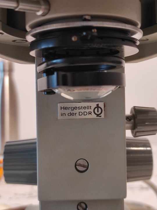
Zeiss Jena Laboval ?3? I think, documentation for the Laboval series online starts and ends with the Laboval 4. By all accounts this is their upper mid range lab scope, with Amplival being the top of the line before you get to big scopes that have to be installed by a technician.
There's a large variety of Zeiss scopes that were manufacturered on this side of the iron curtain, as you can see this is an East German piece. Pretty good condition, scratchy condenser optics but the objectives and eyepiece seem to be in great nick, from a quick inspection, and that's what matters. Eyepieces are 10×'s, Objectives are a 3.2 semiplanar, a 10, a 40 planar (which I think will get a lot of use), and a 100 oil immersion. Pretty normal setup.
I don't have slides and slips yet so I can't do a proper mount, but this is pretty promising for just sliding a sheet of paper into the slide holder. Proper mounting will improve the focus plane immensely. 32× and 100× so far.


The illumination is off-centre and uneven but that's resolvable and anyway it might be fun to move to LED. I also want to build some top illumination brackets for opaque subjects.
I had like. A kiddies toy microscope growing up and I got as far as trying to make it do darkfield with pieces of cardboard, but never something this professional, binocular optics is such a big step up on its own.
The only real issue I've seen so far is that the stage Z axis is very sloppy, huge backlash. Everything has been stuffed with new grease recently so at least it moves smoothly, old scopes and old typewriters both have a tendency to seize if they're forgotten for more than a few months at a time.
I'll swing by the lake and pick up some algae and protist samples later, and I need to order slides and slips. Also I can print some darkfield and oblique illumination filters.
Probably not going to fuck too much with oil immersion, but who knows, also I'll keep an eye out for water immersion objectives.
I think that with an appropriate head replacement and some filter hacking I could get phase contrast microscopy up and running, probably scavenging some Amplival parts. I'd need to see. I can definitely get fluorescence microscopy working with an illumination upgrade. It would also be nice to gut the electronics and put in a simple battery powered illumination system I can charge over USB so I don't have to rely on wall power. Even the stock tungsten lighting is only 5W at 6V so that's easy to swing.
Objectives are DIN 45mm I think, and it sounds like many Eastern Bloc microscopes use standardized head mounts. I'll also be able to print a lot of parts for this, but I'll probably want to get some black filament for optical reasons.
First I want to do some protist sketches, I picked up a protists book at a used bookstore a while ago and it got me really hyped to do protist watching. This is definitely at some level me trying to replace macroscopic wildlife spotting in my life.
20 notes
·
View notes
Text
Types of Microscopes
1. Simple Microscope
2. Compound Microscope
3. Phase Contrast Microscope
4. Fluorescence Microscope
5. Electron Microscope
6. Scanning Electron Microscope (SEM)
7. Transmission Electron Microscope (TEM)
8. Dark Field Microscope
9. Dissecting Microscope (Stereo Microscope)
10. Digital Microscope
11. Scanning Probe Microscope (SPM)
12. Atomic Force Microscope (ATM)
13. Inverted Microscope
14. Acoustic Microscope
15. X-Ray Microscope
16. Polarizing Microscope
17. Metallurgical Microscope
18. Pocket Microscope
19. USB Microscope
20. Confocal Microscope
21. Laser Scanning Microscope
22. Differential Interference Contrast Microscope (DIC)
23. Near-field Scanning Optical Microscope (NSOM)
24. Raman Microscope
25. Super-resolution Microscope
26. Cryo-electron Microscope
27. Time-lapse Microscope
There is a wide range of microscopy techniques and instruments used in various fields of science and research.
#forensic#forensics#criminology#forensic science#evidence#criminalistic#forensic field#crime#forensic science notes#crime scene investigation#electron microscope#microscope
8 notes
·
View notes
Text
Inhibition of EIF4E Downregulates VEGFA and CCND1 Expression to Suppress Ovarian Cancer Tumor Progression by Jing Wang in Journal of Clinical Case Reports Medical Images and Health Sciences
Abstract
This study investigates the role of EIF4E in ovarian cancer and its influence on the expression of VEGFA and CCND1. Differential expression analysis of VEGFA, CCND1, and EIF4E was conducted using SKOV3 cells in ovarian cancer patients and controls. Correlations between EIF4E and VEGFA/CCND1 were assessed, and three-dimensional cell culture experiments were performed. Comparisons of EIF4E, VEGFA, and CCND1 mRNA and protein expression between the EIF4E inhibitor 4EGI-1-treated group and controls were carried out through RT-PCR and Western blot. Our findings demonstrate elevated expression of EIF4E, VEGFA, and CCND1 in ovarian cancer patients, with positive correlations. The inhibition of EIF4E by 4EGI-1 led to decreased SKOV3 cell clustering and reduced mRNA and protein levels of VEGFA and CCND1. These results suggest that EIF4E plays a crucial role in ovarian cancer and its inhibition may modulate VEGFA and CCND1 expression, underscoring EIF4E as a potential therapeutic target for ovarian cancer treatment.
Keywords: Ovarian cancer; Eukaryotic translation initiation factor 4E; Vascular endothelial growth factor A; Cyclin D1
Introduction
Ovarian cancer ranks high among gynecological malignancies in terms of mortality, necessitating innovative therapeutic strategies [1]. Vascular endothelial growth factor (VEGF) plays a pivotal role in angiogenesis, influencing endothelial cell proliferation, migration, vascular permeability, and apoptosis regulation [2, 3]. While anti-VEGF therapies are prominent in malignancy treatment [4], the significance of cyclin D1 (CCND1) amplification in cancers, including ovarian, cannot be overlooked, as it disrupts the cell cycle, fostering tumorigenesis [5, 6]. Eukaryotic translation initiation factor 4E (EIF4E), central to translation initiation, correlates with poor prognoses in various cancers due to its dysregulated expression and activation, particularly in driving translation of growth-promoting genes like VEGF [7, 8]. Remarkably, elevated EIF4E protein levels have been observed in ovarian cancer tissue, suggesting a potential role in enhancing CCND1 translation, thereby facilitating cell cycle progression and proliferation [9]. Hence, a novel conjecture emerges: by modulating EIF4E expression, a dual impact on VEGF and CCND1 expression might be achieved. This approach introduces an innovative perspective to impede the onset and progression of ovarian cancer, distinct from existing literature, and potentially offering a unique therapeutic avenue.
Materials and Methods
Cell Culture
Human ovarian serous carcinoma cell line SKOV3 (obtained from the Cell Resource Center, Shanghai Institutes for Biological Sciences, Chinese Academy of Sciences) was cultured in DMEM medium containing 10% fetal bovine serum. Cells were maintained at 37°C with 5% CO2 in a cell culture incubator and subcultured every 2-3 days.
Three-Dimensional Spheroid Culture
SKOV3 cells were prepared as single-cell suspensions and adjusted to a concentration of 5×10^5 cells/mL. A volume of 0.5 mL of single-cell suspension was added to Corning Ultra-Low Attachment 24-well microplates and cultured at 37°C with 5% CO2 for 24 hours. Subsequently, 0.5 mL of culture medium or 0.5 mL of EIF4E inhibitor 4EGI-1 (Selleck, 40 μM) was added. After 48 hours, images were captured randomly from five different fields—upper, lower, left, right, and center—using an inverted phase-contrast microscope. The experiment was repeated three times.
GEPIA Online Analysis
The GEPIA online analysis tool (http://gepia.cancer-pku.cn/index.html) was utilized to assess the expression of VEGFA, CCND1, and EIF4E in ovarian cancer tumor samples from TCGA and normal samples from GTEx. Additionally, Pearson correlation coefficient analysis was employed to determine the correlation between VEGF and CCND1 with EIF4E.
RT-PCR
RT-PCR was employed to assess the mRNA expression levels of EIF4E, VEGF, and CCND1 in treatment and control group samples. Total RNA was extracted using the RNA extraction kit from Vazyme, followed by reverse transcription to obtain cDNA using their reverse transcription kit. Amplification was carried out using SYBR qPCR Master Mix as per the recommended conditions from Vazyme. GAPDH was used as an internal reference, and the primer sequences for PCR are shown in Table 1.
Amplification was carried out under the following conditions: an initial denaturation step at 95°C for 60 seconds, followed by cycling conditions of denaturation at 95°C for 10 seconds, annealing at 60°C for 30 seconds, repeated for a total of 40 cycles. Melting curves were determined under the corresponding conditions. Each sample was subjected to triplicate experiments. The reference gene GAPDH was used for normalization. The relative expression levels of the target genes were calculated using the 2-ΔΔCt method.
Western Blot
Western Blot technique was employed to assess the protein expression levels of EIF4E, VEGF, and CCND1 in the treatment and control groups. Initially, cell samples collected using RIPA lysis buffer were lysed, and the total protein concentration was determined using the BCA assay kit (Shanghai Biyuntian Biotechnology, Product No.: P0012S). Based on the detected concentration, 20 μg of total protein was loaded per well. Electrophoresis was carried out using 5% stacking gel and 10% separating gel. Subsequently, the following primary antibodies were used for immune reactions: rabbit anti-human polyclonal antibody against phospho-EIF4E (Beijing Boao Sen Biotechnology, Product No.: bs-2446R, dilution 1:1000), mouse anti-human monoclonal antibody against EIF4E (Wuhan Sanying Biotechnology, Product No.: 66655-1-Ig, dilution 1:5000), mouse anti-human monoclonal antibody against VEGFA (Wuhan Sanying Biotechnology, Product No.: 66828-1-Ig, dilution 1:1000), mouse anti-human monoclonal antibody against CCND1 (Wuhan Sanying Biotechnology, Product No.: 60186-1-Ig, dilution 1:5000), and mouse anti-human monoclonal antibody against GAPDH (Shanghai Biyuntian Biotechnology, Product No.: AF0006, dilution 1:1000). Subsequently, secondary antibodies conjugated with horseradish peroxidase (Shanghai Biyuntian Biotechnology, Product No.: A0216, dilution 1:1000) were used for immune reactions. Finally, super-sensitive ECL chemiluminescence reagent (Shanghai Biyuntian Biotechnology, Product No.: P0018S) was employed for visualization, and the ChemiDocTM Imaging System (Bio-Rad Laboratories, USA) was used for image analysis.
Statistical Analysis
GraphPad software was used for statistical analysis. Data were presented as (x ± s) and analyzed using the t-test for quantitative data. Pearson correlation analysis was performed for assessing correlations. A significance level of P < 0.05 was considered statistically significant.
Results
3D Cell Culture of SKOV3 Cells and Inhibitory Effect of 4EGI-1 on Aggregation
In this experiment, SKOV3 cells were subjected to 3D cell culture, and the impact of the EIF4E inhibitor 4EGI-1 on ovarian cancer cell aggregation was investigated. As depicted in Figure 1, compared to the control group (Figure 1A), the diameter of the SKOV3 cell spheres significantly decreased in the treatment group (Figure 1B) when exposed to 4EGI-1 under identical culture conditions. This observation indicates that inhibiting EIF4E expression effectively suppresses tumor aggregation.
Expression and Correlation Analysis of VEGFA, CCND1, and EIF4E in Ovarian Cancer Samples
To investigate the expression of VEGFA, CCND1, and EIF4E in ovarian cancer, we utilized the GEPIA online analysis tool and employed the Pearson correlation analysis method to compare expression differences between tumor and normal groups. As depicted in Figures 2A-C, the results indicate significantly elevated expression levels of VEGFA, CCND1, and EIF4E in the tumor group compared to the normal control group. Notably, the expression differences of VEGFA and CCND1 were statistically significant (p < 0.05). Furthermore, the correlation analysis revealed a positive correlation between VEGFA and CCND1 with EIF4E (Figures 2D-E), and this correlation exhibited significant statistical differences (p < 0.001). These findings suggest a potential pivotal role of VEGFA, CCND1, and EIF4E in the initiation and progression of ovarian cancer, indicating the presence of intricate interrelationships among them.
EIF4E, VEGFA, and CCND1 mRNA Expression in SKOV3 Cells
To investigate the function of EIF4E in SKOV3 cells, we conducted RT-PCR experiments comparing EIF4E inhibition group with the control group. As illustrated in Figure 3, treatment with 4EGI-1 significantly reduced EIF4E expression (0.58±0.09 vs. control, p < 0.01). Concurrently, mRNA expression of VEGFA (0.76±0.15 vs. control, p < 0.05) and CCND1 (0.81±0.11 vs. control, p < 0.05) also displayed a substantial decrease. These findings underscore the significant impact of EIF4E inhibition on the expression of VEGFA and CCND1, indicating statistically significant differences.
Protein Expression Profiles in SKOV3 Cells with EIF4E Inhibition and Control Group
Protein expression of EIF4E, VEGFA, and CCND1 was assessed using Western Blot in the 4EGI-1 treatment group and the control group. As presented in Figure 4, the expression of p-EIF4E was significantly lower in the 4EGI-1 treatment group compared to the control group (0.33±0.14 vs. control, p < 0.001). Simultaneously, the expression of VEGFA (0.53±0.18 vs. control, p < 0.01) and CCND1 (0.44±0.16 vs. control, p < 0.001) in the 4EGI-1 treatment group exhibited a marked reduction compared to the control group.
Discussion
EIF4E is a post-transcriptional modification factor that plays a pivotal role in protein synthesis. Recent studies have underscored its critical involvement in various cancers [10]. In the context of ovarian cancer research, elevated EIF4E expression has been observed in late-stage ovarian cancer tissues, with low EIF4E expression correlating to higher survival rates [9]. Suppression of EIF4E expression or function has been shown to inhibit ovarian cancer cell proliferation, invasion, and promote apoptosis. Various compounds and drugs that inhibit EIF4E have been identified, rendering them potential candidates for ovarian cancer treatment [11]. Based on the progressing understanding of EIF4E's role in ovarian cancer, inhibiting EIF4E has emerged as a novel therapeutic avenue for the disease. 4EGI-1, a cap-dependent translation small molecule inhibitor, has been suggested to disrupt the formation of the eIF4E complex [12]. In this study, our analysis of public databases revealed elevated EIF4E expression in ovarian cancer patients compared to normal controls. Furthermore, through treatment with 4EGI-1 in the SKOV3 ovarian cancer cell line, we observed a capacity for 4EGI-1 to inhibit SKOV3 cell spheroid formation. Concurrently, results from PCR and Western Blot analyses demonstrated effective EIF4E inhibition by 4EGI-1. Collectively, 4EGI-1 effectively suppresses EIF4E expression and may exert its effects on ovarian cancer therapy by modulating EIF4E.
Vascular Endothelial Growth Factor (VEGF) is a protein that stimulates angiogenesis and increases vascular permeability, playing a crucial role in tumor growth and metastasis [13]. In ovarian cancer, excessive release of VEGF by tumor cells leads to increased angiogenesis, forming a new vascular network to provide nutrients and oxygen to tumor cells. The formation of new blood vessels enables tumor growth, proliferation, and facilitates tumor cell dissemination into the bloodstream, contributing to distant metastasis [14]. As a significant member of the VEGF family, VEGFA has been extensively studied, and it has been reported that VEGFA expression is notably higher in ovarian cancer tumors [15], consistent with our public database analysis. Furthermore, elevated EIF4E levels have been associated with increased malignant tumor VEGF mRNA translation [16]. Through the use of the EIF4E inhibitor 4EGI-1 in ovarian cancer cell lines, we observed a downregulation in both mRNA and protein expression levels of VEGFA. This suggests that EIF4E inhibition might affect ovarian cancer cell angiogenesis capability through downregulation of VEGF expression.
Cyclin D1 (CCND1) is a cell cycle regulatory protein that participates in controlling cell entry into the S phase and the cell division process. In ovarian cancer, overexpression of CCND1 is associated with increased tumor proliferation activity and poor prognosis [17]. Elevated CCND1 levels promote cell cycle progression, leading to uncontrolled cell proliferation [18]. Additionally, CCND1 can activate cell cycle-related signaling pathways, promoting cancer cell growth and invasion capabilities [19]. Studies have shown that CCND1 gene expression is significantly higher in ovarian cancer tissues compared to normal ovarian tissues [20], potentially promoting proliferation and cell cycle progression through enhanced cyclin D1 translation [9]. Our public database analysis results confirm these observations. Furthermore, treatment with the EIF4E inhibitor 4EGI-1 in ovarian cancer cell lines resulted in varying degrees of downregulation in CCND1 mRNA and protein levels. This indicates that EIF4E inhibition might affect ovarian cancer cell proliferation and cell cycle progression through regulation of CCND1 expression.
In conclusion, overexpression of EIF4E appears to be closely associated with the clinical and pathological characteristics of ovarian cancer patients. In various tumors, EIF4E is significantly correlated with VEGF and cyclin D1, suggesting its role in the regulation of protein translation related to angiogenesis and growth [9, 21]. The correlation analysis results in our study further confirmed the positive correlation among EIF4E, VEGFA, and CCND1 in ovarian cancer. Simultaneous inhibition of EIF4E also led to downregulation of VEGFA and CCND1 expression, validating their interconnectedness. Thus, targeted therapy against EIF4E may prove to be an effective strategy for treating ovarian cancer. However, further research and clinical trials are necessary to assess the safety and efficacy of targeted EIF4E therapy, offering more effective treatment options for ovarian cancer patients.
Acknowledgments:
Funding: This study was supported by the Joint Project of Southwest Medical University and the Affiliated Traditional Chinese Medicine Hospital of Southwest Medical University (Grant No. 2020XYLH-043).
Conflict of Interest: The authors declare no conflicts of interest.
#Ovarian cancer#Eukaryotic translation initiation factor 4E#Vascular endothelial growth factor A#Cyclin D1#Review Article in Journal of Clinical Case Reports Medical Images and Health Sciences .#jcrmhs
2 notes
·
View notes
Text
X-Ray Grating Market: Key Players and Regional Insights

MARKET INSIGHTS
The global X-Ray Grating Market size was valued at US$ 145.6 million in 2024 and is projected to reach US$ 267.8 million by 2032, at a CAGR of 9.14% during the forecast period 2025-2032. The U.S. market accounted for approximately 32% of global revenue in 2024, while China’s market is expected to grow at a faster pace with 8.3% CAGR through 2032.
X-Ray gratings are precision optical components used to diffract X-rays in analytical instruments. These nanostructured devices play critical roles in phase-contrast imaging, spectroscopy, and medical diagnostics by manipulating X-ray beams at microscopic levels. The market primarily consists of absorption gratings and phase gratings, with absorption variants currently dominating 68% of total revenue share.
Growing adoption in synchrotron facilities and advancements in X-ray microscopy are driving market expansion. However, high manufacturing costs remain a challenge, with premium gratings costing upwards of USD 15,000 per unit. Key manufacturers like SMT and Shimadzu are investing in nanoimprint lithography to improve production efficiency. In 2023, the Paul Scherrer Institute demonstrated a breakthrough in high-efficiency grating fabrication, potentially reducing costs by 40% in coming years.
MARKET DYNAMICS
MARKET DRIVERS
Expanding Medical Imaging Applications Accelerate X-Ray Grating Demand
The global healthcare sector’s accelerating adoption of advanced X-ray imaging technologies is significantly boosting the X-ray grating market. Phase-contrast imaging techniques using X-ray gratings now enable early detection of soft tissue abnormalities with up to 100 times greater sensitivity than conventional radiography. This breakthrough is particularly transformative for mammography and pulmonary diagnostics, where current systems achieve resolutions below 50 micrometers. The technology’s ability to differentiate between tumor types without contrast agents is revolutionizing diagnostic pathways while reducing patient exposure to ionizing radiation by approximately 30-40% compared to traditional CT scans.
Materials Science Breakthroughs Create New Industrial Applications
Beyond healthcare, X-ray gratings are becoming indispensable tools in materials characterization across aerospace, semiconductor, and renewable energy sectors. Recent developments in nano-fabrication techniques allow gratings with periodicities below 100nm, enabling non-destructive testing of advanced composites and battery materials. The automotive industry’s shift toward lightweight materials has driven grating adoption for weld integrity testing, with some manufacturers reporting 25-35% reductions in quality control cycle times. Semiconductor producers increasingly rely on phase-shift gratings for sub-10nm chip defect detection, creating sustained demand from this high-value sector.
Synchrotron Facility Expansion Creates Specialist Demand
The synchronized global expansion of fourth-generation synchrotron facilities presents specialized opportunities for high-performance grating manufacturers. Next-generation light sources like the European XFEL and upgraded APS-U require gratings with dimensional stability below 1nm over meter-scale lengths. This technical challenge has spurred development of silicon carbide and monocrystalline tungsten gratings capable of withstanding 100W/mm² heat loads without deformation. With over 50 major synchrotron facilities operational worldwide and at least 12 upgrade projects underway, specialist grating providers are experiencing compound annual growth exceeding 9% in this niche segment.
MARKET RESTRAINTS
Precision Fabrication Challenges Limit Mass Production Capacity
Despite growing demand, X-ray grating adoption faces significant manufacturing bottlenecks. Producing grating structures with sub-micron periodicity requires specialized cleanroom facilities and e-beam lithography equipment costing upwards of $5 million per system. Even with advanced tools, typical production yields for high-performance gratings rarely exceed 70%, creating supply constraints. The industry’s reliance on small-batch manual alignment processes further exacerbates capacity limitations, with lead times for custom gratings frequently extending beyond six months.
Material Limitations Constrain Performance Parameters
Current grating materials struggle to simultaneously optimize three critical parameters: high diffraction efficiency, thermal stability, and radiation hardness. Silicon gratings offer excellent dimensional precision but degrade rapidly above 500W/mm² fluxes. Gold-coated gratings provide superior heat resistance but exhibit efficiency losses at high X-ray energies. These material limitations force difficult trade-offs in application-specific designs, particularly for emerging techniques like time-resolved X-ray diffraction that require both high flux tolerance and temporal resolution below 10 picoseconds.
MARKET CHALLENGES
Metrology Gaps Impede Quality Assurance Processes
The industry faces persistent challenges in verifying grating specifications after production. Conventional optical microscopy cannot resolve sub-100nm features, while atomic force microscopy throughput remains insufficient for production-quality inspections. This metrology gap creates uncertainties in performance validation, particularly for phase-shift gratings where structural errors as small as 5nm can degrade imaging contrast by 30% or more. Without standardized characterization methods, manufacturers and end-users frequently disagree on acceptance criteria, increasing project risks and warranty exposures.
Intellectual Property Barriers Slow Technology Transfer
Proprietary fabrication methods and overlapping patent claims create minefields for new market entrants. Several critical grating designs remain protected by university-held patents with complex licensing structures, while key processing techniques are closely guarded as trade secrets. This IP landscape discourages collaborative development and makes technology transfer between academic research and commercial production particularly challenging. The resulting innovation bottlenecks are evident in the gradual pace of manufacturing automation adoption across the sector.
MARKET OPPORTUNITIES
Compact Laboratory Sources Expand Addressable Market
The commercialization of benchtop X-ray sources with grating-compatible brilliance creates substantial growth potential. Modern laser-driven plasma sources now achieve spectral brightness exceeding 10¹⁰ photons/s/mm²/mrad² within laboratory footprints, eliminating the need for synchrotron access in many applications. Early adopters report successful grating-based phase contrast imaging implementations with these systems at 10-15% of traditional facility costs. As source technology matures, the total available market for X-ray gratings could expand by 40-60% into academic labs and industrial QA departments previously priced out of the technology.
Multi-layer Gratings Enable New Measurement Modalities
Emerging multi-layer grating architectures promise to unlock novel characterization techniques. Stacked grating designs combining absorption and phase components can simultaneously extract attenuation-, phase-, and dark-field contrast from single exposures – a capability already demonstrated in prototype mammography systems. Similarly, tunable grating systems incorporating MEMS actuators enable adjustable energy filtering, potentially replacing multiple fixed gratings in clinical CT scanners. These innovations could drive grating content per system upwards while creating technical differentiation opportunities for advanced manufacturers.
Additive Manufacturing Opens New Design Possibilities
Advances in nanoscale 3D printing present intriguing possibilities for next-generation grating production. Two-photon polymerization systems now achieve <100nm feature resolution suitable for certain grating applications, while electron beam melting shows promise for direct metal grating fabrication. Although current additive methods cannot yet match lithography-based approaches for critical parameters, they enable previously impossible geometries like tapered grating profiles and integrated mounting structures. Several research groups have demonstrated prototypes with 10-15% efficiency gains from these unconventional designs, suggesting a disruptive potential that warrants industry attention.
X-RAY GRATING MARKET TRENDS
Technological Advancements in X-Ray Imaging Driving Market Expansion
The X-Ray grating market is experiencing significant growth due to rapid advancements in X-ray imaging technologies, particularly in medical diagnostics and material science applications. The shift toward high-resolution phase-contrast imaging systems has created substantial demand for precision X-ray gratings. Recent developments include novel fabrication techniques using deep reactive ion etching (DRIE) and nanoimprint lithography, enabling production of gratings with sub-micron feature sizes. These innovations are critical for next-generation X-ray interferometry applications, where the global market is projected to grow at a CAGR of 8-10% through 2032. Furthermore, the integration of artificial intelligence in X-ray image reconstruction algorithms is enhancing the performance demands placed on grating components.
Other Trends
Expansion of Synchrotron and Laboratory-Based Applications
While medical imaging remains the dominant application segment, synchrotron facilities and laboratory X-ray systems are emerging as key growth areas. There are currently over 50 synchrotron light sources operational worldwide, with several new facilities under construction across Asia and Europe. These large-scale research installations require advanced grating systems for high-precision X-ray analysis techniques such as X-ray fluorescence and small-angle X-ray scattering. The market for laboratory X-ray instruments incorporating grating optics is estimated to reach $200-250 million annually by 2027, driven by increasing adoption in pharmaceutical research and nanotechnology characterization.
Materials Innovation and Manufacturing Challenges
The industry faces both opportunities and constraints in materials development. Silicon remains the predominant material for X-ray gratings, accounting for approximately 65-70% of all gratings produced. However, emerging materials such as diamond and high-Z metals are gaining traction for specialized applications requiring extreme durability or high-energy X-ray performance. The transition to these advanced materials presents manufacturing challenges, with yields for high-quality diamond gratings currently below 40% in most production facilities. Nevertheless, ongoing process optimization efforts are expected to improve both quality and cost-effectiveness as the technology matures.
The competitive landscape continues to evolve, with established players investing in large-area grating fabrication capabilities to meet the needs of whole-body phase-contrast medical imaging systems. Meanwhile, startup companies are pioneering novel approaches to grating design, including adaptive and tunable grating solutions that could revolutionize X-ray analysis methodologies in the coming decade.
COMPETITIVE LANDSCAPE
Key Industry Players
Leading Manufacturers Focus on Precision and Innovation in X-Ray Grating Production
The global X-ray grating market exhibits a semi-fragmented competitive structure, blending multinational corporations with specialized regional suppliers. SMT (Supermirror Technologies) has emerged as a dominant force due to its high-precision grating solutions and robust manufacturing capabilities in North America and Europe. Their technology enables applications in advanced synchrotron facilities and medical imaging systems.
NTT Advanced Technology Corporation and XRNanotech have carved significant market shares through their patented nano-fabrication techniques. These companies accounted for approximately 22% of combined revenue share in 2024, serving major research institutions and industrial clients across Asia-Pacific markets.
The competitive intensity is further amplified by ongoing R&D investments in phase contrast imaging technologies. Unlike conventional absorption gratings, phase grating solutions are gaining traction in materials science applications because of their superior sensitivity to low-density specimens.
Meanwhile, European players like Microworks GmbH and Gitterwerk GmbH differentiate through customized grating solutions for synchrotron beamlines. Their strategic collaborations with academic institutions have strengthened their footprint in the scientific research segment, which represents over 35% of total application demand.
Recent competitive developments include SHIMADZU’s January 2024 launch of their ultra-high resolution X-ray Talbot-Lau interferometry gratings, specifically engineered for compact laboratory systems. This mirrors broader industry trends where manufacturers balance performance enhancements with form factor optimization for benchtop applications.
List of Key X-Ray Grating Companies Profiled
SMT (Supermirror Technologies) (Germany)
NTT Advanced Technology Corporation (Japan)
XRNanotech (U.S.)
SHIMADZU Corporation (Japan)
Paul Scherrer Institute PSI (Switzerland)
ASICON Tokyo Ltd. (Japan)
HORIBA France SAS (France)
Inprentus (U.S.)
Microworks GmbH (Germany)
Gitterwerk GmbH (Germany)
Wasatch Photonics (U.S.)
LightTrans International (Germany)
Segment Analysis:
By Type
Absorption Grating Segment Leads Due to High Demand in Medical and Industrial Imaging Applications
The market is segmented based on type into:
Absorption Grating
Phase Grating
By Application
Science Segment Dominates Owing to Increased Utilization in Research Laboratories and Academic Institutions
The market is segmented based on application into:
Chemical
Science
Others
By End-User
Healthcare Sector Holds Significant Share Driven by Advancements in Medical Imaging Technologies
The market is segmented based on end-user into:
Healthcare
Industrial
Research institutes
Others
Regional Analysis: X-Ray Grating Market
North America The North American X-ray grating market is driven by robust healthcare expenditure and strong research & development activities in medical imaging technologies. The U.S. leads the region with a market size estimated at $ million in 2024, supported by advanced diagnostic infrastructure in hospitals and research institutions. Major players like SMT and Wasatch Photonics maintain strong market positions, catering to both medical and industrial applications. Phase gratings are gaining traction due to their superior resolution capabilities in synchrotron facilities, though absorption gratings remain dominant in conventional X-ray equipment. Challenges include high production costs and stringent FDA approval processes for medical-grade components.
Europe Europe’s market thrives on cutting-edge scientific research and precision engineering capabilities. Germany and France collectively account for over 40% of regional demand, with institutes like Paul Scherrer Institute PSI driving innovation in phase contrast imaging. The market benefits from cross-border academic collaborations and EU-funded research projects in nanotechnology. However, the fragmentation of standards across countries creates compliance complexities for manufacturers. Recent developments include the adoption of high-efficiency gratings in airport security scanners and automotive NDT applications. Environmental regulations on material usage (particularly lead-based components) are reshaping product specifications across the region.
Asia-Pacific Asia-Pacific exhibits the highest growth potential, projected to reach $ million by 2032 primarily due to China’s expanding healthcare infrastructure. Local manufacturers like XRNanotech and Top-Unistar Science & Technology are capturing market share through cost-competitive solutions, though Japanese firms (SHIMADZU, ASICON Tokyo) dominate premium segments. Two distinct trends emerge: budget-conscious hospitals opt for conventional absorption gratings, while research centers invest in advanced phase gratings for materials science applications. India’s market grows at 8% CAGR, fueled by public-private partnerships in medical imaging and government initiatives like Make in India. However, inconsistent quality standards and intellectual property concerns remain key challenges.
South America The region shows moderate growth, with Brazil accounting for 60% of market activity. Limited local manufacturing capabilities create dependence on imports from North America and Europe, particularly for specialized applications in oil & gas pipeline inspection. Economic instability in Argentina and Venezuela hinders market expansion, though Colombia and Chile demonstrate steady demand from mining and petrochemical industries. Market opportunities exist in upgrading aging hospital imaging equipment, but currency fluctuations and complex import procedures delay procurement cycles. The lack of regional technical expertise in grating maintenance also impacts aftermarket services.
Middle East & Africa This emerging market centers around GCC countries, where healthcare modernization projects and oilfield inspection needs drive demand. The UAE and Saudi Arabia collectively invest over $500 million annually in medical imaging equipment, creating opportunities for grating suppliers. However, the absence of local production facilities results in complete import reliance at premium prices. Key restraints include limited awareness of advanced grating technologies and budget prioritization toward complete imaging systems rather than components. South Africa shows potential in mining applications, though political and economic uncertainties curb sustained market growth.
Report Scope
This market research report provides a comprehensive analysis of the global and regional X-Ray Grating markets, covering the forecast period 2025–2032. It offers detailed insights into market dynamics, technological advancements, competitive landscape, and key trends shaping the industry.
Key focus areas of the report include:
Market Size & Forecast: Historical data and future projections for revenue, unit shipments, and market value across major regions and segments. The Global X-Ray Grating market was valued at USD 220.8 million in 2024 and is projected to reach USD 340.6 million by 2032.
Segmentation Analysis: Detailed breakdown by product type (Absorption Grating, Phase Grating), application (Chemical, Science, Others), and end-user industry to identify high-growth segments and investment opportunities. The Absorption Grating segment is expected to reach USD 198.2 million by 2032.
Regional Outlook: Insights into market performance across North America, Europe, Asia-Pacific, Latin America, and the Middle East & Africa, including country-level analysis. The U.S. market size is estimated at USD 78.4 million in 2024, while China is projected to reach USD 92.1 million by 2032.
Competitive Landscape: Profiles of leading market participants including SMT, NTT Advanced Technology Corporation, XRNanotech, and SHIMADZU, covering their product offerings, R&D focus, manufacturing capacity, pricing strategies, and recent developments.
Technology Trends & Innovation: Assessment of emerging technologies in X-ray optics, nano-fabrication techniques, and evolving industry standards for grating-based X-ray imaging.
Market Drivers & Restraints: Evaluation of factors driving market growth along with challenges such as high manufacturing costs and technical complexities in grating fabrication.
Stakeholder Analysis: Insights for component suppliers, OEMs, system integrators, investors, and policymakers regarding the evolving X-ray grating ecosystem and strategic opportunities.
Related Reports:https://semiconductorblogs21.blogspot.com/2025/06/laser-diode-cover-glass-market-valued.htmlhttps://semiconductorblogs21.blogspot.com/2025/06/q-switches-for-industrial-market-key.htmlhttps://semiconductorblogs21.blogspot.com/2025/06/ntc-smd-thermistor-market-emerging_19.htmlhttps://semiconductorblogs21.blogspot.com/2025/06/lightning-rod-for-building-market.htmlhttps://semiconductorblogs21.blogspot.com/2025/06/cpe-chip-market-analysis-cagr-of-121.htmlhttps://semiconductorblogs21.blogspot.com/2025/06/line-array-detector-market-key-players.htmlhttps://semiconductorblogs21.blogspot.com/2025/06/tape-heaters-market-industry-size-share.htmlhttps://semiconductorblogs21.blogspot.com/2025/06/wavelength-division-multiplexing-module.htmlhttps://semiconductorblogs21.blogspot.com/2025/06/electronic-spacer-market-report.htmlhttps://semiconductorblogs21.blogspot.com/2025/06/5g-iot-chip-market-technology-trends.htmlhttps://semiconductorblogs21.blogspot.com/2025/06/polarization-beam-combiner-market.htmlhttps://semiconductorblogs21.blogspot.com/2025/06/amorphous-selenium-detector-market-key.htmlhttps://semiconductorblogs21.blogspot.com/2025/06/output-mode-cleaners-market-industry.htmlhttps://semiconductorblogs21.blogspot.com/2025/06/digitally-controlled-attenuators-market.htmlhttps://semiconductorblogs21.blogspot.com/2025/06/thin-double-sided-fpc-market-key.html
0 notes
Text
Chapter 10 in Part 2 of Process and Reality by Alfred North Whitehead. Probably the singular most exciting and sophisticated passages I've ever read

Whitehead here introduces two poles of identity philosophy that runs through the Western tradition: movement or stasis. dynamic becoming or static being.

Whitehead further examines the notion of "flux" and the relationship of movement in the universe to consciousness with brief remarks on Plato, Hume, Aristotle, Descartes, and Bergson

Whitehead suggests that Western philosophy discovered but never made conscious of the discovery that there are actually two kinds of fluency in the world: the microcosm and the macrocosm. The flowing inward of the Many into the unique, novel One, and the flowing outward of the One into the Many. Concrescence is the name for this process of subjective novelty and unification within the diverse Universe

"Concrescence is the name for the process in which the universe of many things acquires an individual unity in a determinate relegation of each item of the Many to its subordination in the constitution of the novel One." So far as an actual occasion is analyzable into component parts, this includes a process of feeling constituting (1) the actual occasions felt; (2) the eternal objects felt; (3) the feelings felt; (4) Its own subjective forms of intensity culminating in a satisfaction: "This final unity is termed the tsatisfaction.' The satisfaction is the culmination of the concrescence into a completely determinate matter of fact. In any of its antecedent stages, the concrescence exhibits sheer indetermination as to the nexus between its many components.

This multistage process is broken down even more by Whitehead into (i) the responsive phase and (ii) the supplemental stage, that leads us finally to the satisfaction. In the responsive phase, "the phase of pure reception of the actual world in its guise of objective datum for aesthetic synthesis. In this phase there is the mere reception of the actual world as a multiplicity of private centres of feeling, implicated in a nexus of mutual presupposition."
Whereas in the supplemental phase, "the many feelings, derivatively felt as alien, are transformed into a unity of aesthetic appreciation immediately felt as private. This is the incoming of appetition, which in its higher exemplifications we term vision. In the language of physical science, the scalar form overwhelms the original vector form: the origins become subordinate to the individual experience. The vector form is not lost, but is submerged as the foundation of the scalar superstructure."


In this next part, Whitehead breaks down the supplemental phase into two subphases: (1) aesthetic supplement; and (2) intellectual supplement. As he notes, if both subphases are trivial, the whole transmission of feelings passes through with little modification and augmentation. This part of the Concrescence urges in the dimensional axis of width of contrast and depth of intensity. "There is an emotional appreciation of the contrasts and rhythms inherent in the unification of the objective content in the concrescence" meaning that there is an actual felt sensation of differentiation of sense data with a gradation of consciousness of its vector origin. This elicits the second subphase: An eternal object realized in respect to its pure potentiality as related to determinate logical subjects is termed a 'propositional feeling' in the mentality of the actual occasion in question. The consciousness belonging to an actual occasion is its sub-phase of intellectual supplementation, when that sub-phase is not purely trivial. This sub-phase is the eliciting, into feeling, of the full contrast between mere propositional potentiality and realized fact."

Thus each actual entity, although complete so far as concerns its microscopic process, is yet incomplete by reason of its objective inclusion of the macroscopicprocess. It really experiences a future which must be actual, although the completed actualities of that future are undetermined. In this sense, each actual occasion experiences its own objective immortality.
#morphogenesis#process philosophy#mesmerism#alfred north whitehead#platonic#metaphysics#panpsychism#panentheism#philosophy#ontology#epistemology
0 notes
Text
Live Cell Monitoring Market Expands Rapidly With Advances in Microscopy and Biosensor Applications
The live cell monitoring market has gained significant traction over the past decade, driven by rapid advances in cellular imaging technologies and increased demand for real-time, high-resolution data in biological research and drug development. This market focuses on technologies and systems that allow researchers to observe living cells over time, without disrupting their natural processes. It has applications across pharmaceutical development, cancer research, stem cell biology, immunology, and more.

Market Overview
Live cell monitoring involves tracking and analyzing the behavior, structure, and function of cells in real-time. Unlike fixed-cell methods, this technology enables researchers to study dynamic cellular processes such as proliferation, migration, apoptosis, and intracellular signaling under natural physiological conditions.
The global live cell monitoring market is witnessing robust growth, and analysts project a compound annual growth rate (CAGR) of over 8% through the next five years. The expansion of pharmaceutical R&D, increasing adoption of high-content screening methods, and growing interest in personalized medicine are key contributors to this upward trend.
Key Technologies Driving Growth
The market is fueled by several core technologies, including:
Live Cell Imaging Systems: These use advanced microscopy (fluorescence, phase contrast, confocal, etc.) to visualize living cells with high spatial and temporal resolution.
Cell-Based Assays: These assays measure biochemical or cellular functions and are essential for high-throughput screening in drug discovery.
Fluorescent Biosensors and Labels: These tools enable researchers to monitor specific molecular events inside cells in real time.
Automated Cell Analyzers and Incubation Systems: These integrated platforms allow continuous monitoring without disturbing cell cultures, enhancing efficiency and data quality.
Market Segmentation
The live cell monitoring market is segmented based on:
Product Type: Instruments (microscopes, image analysis systems), consumables (reagents, kits), and software.
Application: Cancer research, stem cell research, immunology, neuroscience, and drug discovery.
End User: Academic and research institutes, pharmaceutical and biotechnology companies, and contract research organizations (CROs).
Among these, pharmaceutical and biotechnology companies hold a dominant share due to the critical role of live cell assays in evaluating drug efficacy and toxicity in preclinical stages.
Regional Insights
North America remains the largest market, thanks to its well-established pharmaceutical industry, strong funding for life science research, and early adoption of advanced imaging tools. Europe follows closely, with countries like Germany and the UK leading in biomedical research.
The Asia-Pacific region is expected to witness the highest growth during the forecast period. Increasing government initiatives, expanding biopharma industry, and growing investment in academic research—especially in China, India, and South Korea—are the key factors driving regional expansion.
Challenges and Opportunities
Despite strong growth, the market faces several challenges. High equipment costs, complex data analysis requirements, and the need for skilled personnel can hinder adoption, especially in low-resource settings. Moreover, standardization issues in live cell assay protocols can lead to variability in results across labs.
However, ongoing developments in AI-driven image analysis, machine learning for pattern recognition, and cloud-based data sharing present exciting opportunities. These innovations aim to make live cell monitoring more accessible, automated, and user-friendly.
Additionally, the increasing focus on organ-on-a-chip technologies and 3D cell culture models is expected to complement live cell monitoring, expanding its utility in predictive toxicology and disease modeling.
Future Outlook
The future of the live cell monitoring market looks promising. As biological sciences continue to demand more precise, real-time insights, live cell monitoring is poised to become a standard tool in both basic and applied research settings.
Strategic collaborations between research institutions and technology developers, along with rising investment in precision medicine and biologics, will continue to shape the evolution of this market. With AI integration and automation enhancing the capabilities of live cell imaging systems, the next few years could usher in a new era of cell biology research that is faster, more accurate, and more insightful than ever before.
0 notes
Text
Electronic Grade HFE-347 Market, Global Outlook and Forecast 2025-2032
Market Size
The global Electronic Grade HFE-347 market stood at USD 46 million in 2023, and it is projected to reach USD 96.66 million by 2032, growing at a CAGR of 8.60% during the forecast period. This growth rate reflects increasing demand from the electronics and precision cleaning industries, which are seeking efficient and environmentally safer solvents.
North America alone accounted for USD 13.82 million in 2023 and is expected to grow at a CAGR of 7.37% from 2025 to 2032, underscoring strong regional investments in advanced electronics manufacturing and high-purity material use.
The upward trend is supported by the expansion of the semiconductor sector, where ultra-pure solvents like HFE-347 are indispensable. Historical data reveal a consistent demand growth over the past decade, driven by miniaturization in electronics and the increasing need for residue-free cleaning agents. The market trajectory is further catalyzed by tightening environmental regulations against traditional solvents, favoring fluorinated alternatives like HFE-347.
Unlock Data-Driven Decisions
Electronic Grade HFE-347, also known as HFE Electronic Grade, is a hydrofluoroether-based solvent known for its high purity, low toxicity, non-flammability, and excellent material compatibility. It is widely used as a cleaning agent in the electronics, aerospace, and precision equipment industries due to its ability to clean delicate surfaces without damaging them. HFE-347 is particularly valuable in removing oils, greases, and particulates from semiconductors, hard disk drives, circuit boards, and other sensitive electronics components.
This solvent is engineered to meet stringent purity standards required in cleanroom environments, making it suitable for processes where even microscopic contamination is unacceptable. Additionally, Electronic Grade HFE-347 is a preferred alternative to ozone-depleting substances and volatile organic compounds (VOCs), aligning with global sustainability and safety mandates.
Market Dynamics
The Electronic Grade HFE-347 market is currently experiencing a phase of accelerated transformation fueled by several key dynamics. The ongoing global transition toward miniaturized and high-performance electronic components is amplifying the need for superior cleaning agents capable of operating in controlled environments. The demand for high-purity solvents is particularly evident in semiconductor fabrication facilities and printed circuit board (PCB) manufacturing plants, where precision and contamination control are paramount.
One of the most prominent drivers of the market is the shift from conventional solvents to environmentally safer alternatives. Traditional chlorinated solvents, such as CFCs and HCFCs, have faced increasing regulatory scrutiny due to their ozone-depleting and global warming potentials. In contrast, HFE-347 is non-ozone depleting and has a low global warming potential (GWP), making it compliant with international environmental regulations like the Montreal Protocol and Kyoto Protocol. This regulatory support has significantly boosted its adoption.
Furthermore, consumer electronics and automotive electronics sectors are expanding rapidly, particularly in Asia-Pacific, thereby driving demand for high-purity solvents. The proliferation of advanced technologies like 5G, AI, and IoT has heightened the sensitivity of electronic components, necessitating meticulous cleaning processes. These trends reinforce the strategic role of HFE-347 in ensuring optimal product performance and reliability.
From a supply chain perspective, the production of Electronic Grade HFE-347 is concentrated among a few key manufacturers with advanced fluorochemical capabilities, such as AGC Chemicals and Daikin Industries. These companies are investing in research to enhance the solvent’s performance parameters and to reduce production costs, thereby making it more accessible for broader applications.
However, the market also faces certain restraints. The high production cost of fluorinated solvents and their dependency on specialized manufacturing infrastructure limit the entry of new players. Moreover, any changes in fluorochemical regulations or supply chain disruptions, such as those experienced during the COVID-19 pandemic, can significantly impact the global supply and pricing dynamics.
Nonetheless, opportunities are emerging in niche markets such as aerospace component cleaning, medical device manufacturing, and defense electronics, where performance and compliance outweigh cost considerations. The increasing importance of green chemistry and sustainability also opens doors for next-generation HFE solvents, reinforcing the growth trajectory of the Electronic Grade HFE-347 market.
Global Electronic Grade HFE-347 Market: Market Segmentation Analysis
This report provides a deep insight into the global Electronic Grade HFE-347 market, covering all its essential aspects. This ranges from a macro-overview of the market to micro details of the market size, competitive landscape, development trend, niche market, key market drivers and challenges, SWOT analysis, value chain analysis, etc.
The analysis helps the reader to shape the competition within the industries and strategies for the competitive environment to enhance the potential profit. Furthermore, it provides a simple framework for evaluating and assessing the position of the business organization. The report structure also focuses on the competitive landscape of the Global Electronic Grade HFE-347 Market. This report introduces in detail the market share, market performance, product situation, operation situation, etc., of the main players, which helps the readers in the industry to identify the main competitors and deeply understand the competition pattern of the market. In a word, this report is a must-read for industry players, investors, researchers, consultants, business strategists, and all those who have any kind of stake or are planning to foray into the Electronic Grade HFE-347 market in any manner.
Unlock Data-Driven Decisions
Market Segmentation (by Application)
Solvent
Cleaner
Others
Market Segmentation (by Type)
Purity 99%
Purity 99.5%
Others
Key Company
AGC Chemicals
Daikin Industries
Fujian Sannong New Materials
Zhejiang Juhua
ZhongFu Chemical Material Technology
Shandong Hua Fluorochemical
Geographic Segmentation
North America (USA, Canada, Mexico)
Europe (Germany, UK, France, Russia, Italy, Rest of Europe)
Asia-Pacific (China, Japan, South Korea, India, Southeast Asia, Rest of Asia-Pacific)
South America (Brazil, Argentina, Columbia, Rest of South America)
The Middle East and Africa (Saudi Arabia, UAE, Egypt, Nigeria, South Africa, Rest of MEA)
Regional Analysis
North America
North America holds a significant share in the Electronic Grade HFE-347 market, driven by strong demand from advanced electronics and aerospace industries in the U.S. and Canada. In 2023, the region contributed USD 13.82 million to the global market. The regional growth is reinforced by robust R&D activities, favorable regulatory frameworks supporting sustainable chemicals, and the presence of leading electronics manufacturers.
The U.S. in particular is seeing an increase in investments toward semiconductor fabs, such as the CHIPS and Science Act, which allocates substantial funds for domestic chip production. This is expected to further boost the demand for high-purity solvents like HFE-347 in the years ahead.
Europe
Europe remains a mature but steady market, supported by a focus on sustainability and precision engineering. Countries like Germany, France, and the UK are emphasizing clean manufacturing processes, which align with the use of HFE-347. The European Union's stringent chemical regulations (REACH) also push industries to adopt safer solvent alternatives.
Asia-Pacific
Asia-Pacific is the fastest-growing region, led by China, Japan, South Korea, and India. This region is the epicenter of electronics manufacturing, particularly semiconductors and consumer electronics. With increasing cleanroom facility setups and growing export of high-tech electronics, the demand for Electronic Grade HFE-347 is expected to surge.
In China, favorable industrial policies and investments in smart manufacturing have created a conducive environment for the adoption of high-purity cleaning agents. Similarly, Japan and South Korea continue to innovate in semiconductor technologies, further driving market growth.
South America and MEA
These regions are emerging markets with limited but growing adoption. Brazil and Saudi Arabia are investing in technology parks and electronics manufacturing, which may stimulate future demand. However, the lack of local manufacturing capabilities and higher import costs remain challenges.
FAQ Section:
1. What is the current market size of the Electronic Grade HFE-347 market?
As of 2023, the market size is estimated at USD 46 million, projected to reach USD 96.66 million by 2032.
2. Which are the key companies operating in the Electronic Grade HFE-347 market?
Major players include AGC Chemicals, Daikin Industries, Fujian Sannong New Materials, Zhejiang Juhua, ZhongFu Chemical Material Technology, and Shandong Hua Fluorochemical.
3. What are the key growth drivers in the Electronic Grade HFE-347 market?
The primary drivers are the rising demand for high-purity solvents in electronics manufacturing, increasing environmental regulations, and growth in semiconductor and precision device industries.
4. Which regions dominate the Electronic Grade HFE-347 market?
North America and Asia-Pacific are leading regions, with Asia-Pacific showing the fastest growth due to extensive electronics manufacturing.
5. What are the emerging trends in the Electronic Grade HFE-347 market?
Trends include the adoption of green solvents, investment in semiconductor fabs, and expanding use in aerospace and medical device cleaning applications.
Unlock Data-Driven Decisions
0 notes
Text
Evolution, Principle and Application of the Optical Microscope The application of optical microscopy has grown tremendously over the last few decades, this has been so in various disciplines where micron and submicron level investigations are applicable. The spreading out of fluorescence microscopy in research and laboratory applications has been fast-tracked by the instantaneous development of new fluorescent labels. Microscopists have also been able to get quantitative measurements faster and efficiently due to the developments in digital imaging and analysis. It is also possible to obtain very thin optical sections when optical microscopy is enhanced using digital video, the application of confocal optical systems is as well becoming common in a number of major research institutions. Before the nineteenth century, microscopists faced various shortcomings including, optical aberration, blurred images, and poor lens design (Davidson and Abramowitz, 2009). However, in the mid-nineteenth century there was partial correction to aberration through the use of Lister and Amici achromatic objectives. This led to a reduction of the chromatic aberration and raised numerical apertures to around 0.65 for dry objectives and up to 1.25 for homogenous immersion objectives (Bradbury, 1967). Ernst Abbe's and Carl Zeiss also worked together in 1886 to produce apochromatic objectives which were based on sound optical principles and lens design, this was a first one of its kind (Zeiss Group Microscopes Business Unit, 1996). With these advanced objectives, it was possible to obtain images having reduced spherical aberration without color distortions but at high numerical apertures. Evolution of the optical microscope Towards the end of the nineteenth century, Professor August Kohler developed a method of illumination which intended to optimize photomicrography thereby giving microscopists the opportunity of fully utilizing the resolving power of Abbe's objectives. It is within the last decade of the nineteenth century that various innovations in optical microscopy were made, such as metallographic microscopes, anastigmatic photo lenses, binocular microscopes with image-erecting prisms, and the first stereomicroscope (Zeiss Group Microscopes Business Unit, 1996). Further advancements were made in the early twentieth century such as par focalization of objectives by manufacturers which gave the microscopists the advantage of retaining the image in focus while exchanging objectives on the rotating nosepiece. In 1824, a LeChatelier-style metallograph with infinity-corrected optics was introduced by Zeiss, but this method took time to be widely applied. Zeiss later on, just before the beginning of Second World War came up with a number of prototype phase contrast microscopes based on Frits Zernike's optical principles, these microscopes were later modified leading to the development of the first time-lapse cinematography of cell division photographed with phase contrast optics (Davidson and Abramowitz, 2009). This technique which enhanced contrast was not immediately recognized until 1950s when it received a universal acceptance and many biologists still prefer it to-date. The Wollaston prism design was improved by physicist Georges Normarski giving rise to another strong contrast-generating microscopy theory in 1955. This new technique, commonly known as Nomarski interference or differential interference contrast (DIC) microscopy coupled with phase contrast has given scientists a chance of exploring various arenas in biology using living cells or unstained tissues. Another method of increasing contrast was introduced by Robert Hoffman (Hoffman, 1977), this utilized the advantage of phase gradients near cell membranes, a technique now referred to as Hoffman Modulation Contrast. Until the late 1980s, most microscopes had fixed mechanical tube lengths (between 160 to 210 millimeters), after which the infinity-corrected optics was largely adopted. Fundamentals of Image Formation In considering the optical microscope, when light produced by the microscope lamp is directed to go through the condenser and then through the specimen, a portion of the light will go around and through the specimen without experiencing any disturbance in its path, thus referred to as direct light or undeviated light. The light that passes around the specimen to form the background light is also undeviated light. A portion of the light that passes through the specimen encountering parts of the specimen is deviated. This deviated light compared to the undeviated light has half wavelength or is 180 degrees out of step. This leads to destructive interference with the direct light at the intermediate image plane found at the fixed diaphragm of the eyepiece. This image is further magnified by the eye lens of the eye piece and finally projected onto the retina, the film plane of a camera, or the surface of a light sensitive chip. Basically, the objective projects the direct or undeviated light spreading it evenly across the whole image plane at the diaphragm of the eyepiece. This diffracted light is then focused at various localized points on the same image plane where there occurs destructive interference and reduction of intensity giving rise to relatively dark areas. It is these light and dark patterns that are recognized as image of the specimen (Davidson and Abramowitz). Since human eyes are sensitive to variations in brightness, the image is seen as a relatively realistic reconstitution of the original specimen. Image formation is thus based on the principle combining or manipulating direct and diffracted light. The rear focal plane of the objective and the front focal plane of the substage condenser then become significant locations for such manipulation. Various contrast improvement methods in optical microscopy are based on this core principle, this is particularly important when it comes to high magnification of small details whose size are close to the wavelength of light. The figure below shows a diffraction spectra generated at the rear focal plane of the objective by undeviated and diffracted light (Davidson and Abramowitz, 2009). Figure 1 : (a) Spectra visible through a focusing telescope at the rear focal plane of an objective. (b) Schematic diagram of light both diffracted and undeviated by a line grating on the microscope Kohler Illumination In microscopy and critical photomicrography it is very important that specimen is properly illuminated for purposes of achieving high-quality images. August Kohler first introduced an elaborate procedure for microscope illumination in 1893, this was to give optimum specimen illumination. With this technique, users of the microscope were able to achieve a uniformly bright and glare free specimen thus utilizing the microscope adequately. In most modern microscopes, the collector lens and other optical parts built into the base are such that they will project an enlarged and focused image of the lamp filament onto the plane of the aperture diaphragm of a properly positioned substage condenser. The angle of the light rays emerging from the condenser is controlled by closing and opening the condenser diaphragm thus reaching the specimen from all azimuths. Since the focusing of the light source is not done at the specimen level, a grainless and extended illumination at specimen level is achieved, this is free from deterioration caused by dust and imperfections on the glass surfaces of the condenser (Davidson and Abramowitz, 2009). The resulting numerical aperture of the microscope system is determined by the opening size of the condenser aperture diaphragm and the aperture of the objective. On opening the condenser diaphragm, the numerical aperture of the microscope is increased giving rise to greater light transmittance and resolving power. The parallel light rays that pass through and illuminate the specimen are focused at the rear focal plane of the objective where there is simultaneous observation of the image of the variable condenser aperture diaphragm and the light source. Figure 2 : Light paths in Kohler Illumination The figure below shows light paths in Kohler illumination. The left side illustrates illuminating ray paths while the right side are image-forming ray paths. When the lamp emits light it goes through a collector lens and subsequently field diaphragm. The size and shape of the illumination cone on the specimen plane is determined by the aperture diaphragm in the condenser. Before the light is focused at the back focal plane of the objective, it passes through the specimen and eventually is magnified by the ocular and finally into the eye (Davidson and Abramowitz, 2009). Microscope Objectives, Eyepieces, Condensers, and Optical Aberrations Objectives The design of the finite microscope objectives is such that they should project a diffraction-limited image at a fixed plane that is determined by the microscope tube length and located at a pre-specified distance from the rear focal plane of the objective. The imaging of the specimens happens at a very short distance beyond the front focal plane of the objective through a medium of defined refractive index, normally air, water, glycerin, or specialized immersion oils (Davidson and Abramowitz, 2009). In order to meet the performance needs of specialized imaging methods, microscope manufacturers provide a wide range of objective designs. These designs also compensate for thickness of cover glass and increase the effective working distance of the objective. The most commonly used design now is the infinity-corrected objectives which project imaging rays in parallel bundles from every azimuth to infinity. In order to focus the image at the intermediate image plane, a tube lens is necessary in the light path. Optical Aberrations Artifacts arising from the interaction of light with glass lenses lead to what is known as aberrations or lens errors in optical microscopy. There are two major causes of aberration that have been identified: geometrical or spherical aberrations, and chromatic aberrations. The first cause relates to the spherical nature of the lens and approximation used to obtain the Gaussian lens equation, while the second one arises from the variation in the refractive indices of the wide range of frequencies existing in visible light (Davidson and Abramowitz, 2009). Generally, optical aberrations bring about faults in the features of an image that is being observed under a microscope. Spherical aberration: These artifacts are experienced when light waves passing through the periphery and those passing closer to the center are not brought into identical focus. The waves passing closer to the center undergo a slight refraction while those in the periphery are greatly refracted giving rise to different focal points along the optical axis (Davidson and Abramowitz, 2009). Since this artifact makes the image of the specimen to spread out instead of being focused, it is considered as one of the most serious resolutions artifacts. In order to reduce these lens defects, the outer edged of the lens can be limited from exposure to light using diaphragms and also by using aspherical lens surfaces within the system. Chromatic aberration: The fact that lights is composed of numerous wavelengths is the cause of this optical defect. These different wavelengths of light are refracted differently when they pass through a convex lens depending on their frequency. Blue light experiences the greatest refraction then green and red lights, this is referred to as dispersion. Since the lens is not capable of bringing all colors into a common focus, the resultant is a slightly different image size and focal point for each predominant wavelength group. The outcome will be an image surrounded by color fringes (Davidson and Abramowitz, 2009). When the lens thickness, curvature, refractive index and dispersion are properly combined then the doublet reduces chromatic aberration by bringing two of the wavelength groups into a common focal plane. Introducing fluorspar into the glass formulation used to fabricate the lens will bring the three colors red, green, and blue into a single focal point resulting in a negligible amount of chromatic aberration. Eyepieces Eyepieces or oculars are used together with microscope objectives to increase the magnification of the intermediate image so that specimen details can be observed. In order to get best results in microscopy, objectives must be used together with the appropriate eyepieces. There are two types of eyepieces which are categorized using the lens and diaphragm arrangement, these are the negative and positive eyepieces. The negative eyepiece have the internal diaphragm located between the lenses while that of the positive eyepiece is located below the lenses. The negative eyepieces have two lenses: the upper lens closest to the observer's eyes (eye-lens) and the lower lens (field lens). The positive eyepiece has an eye lens, but the field lens is mounted with the curved surface facing towards the eye lens (Davidson and Abramowitz, 2009). Condensers The work of the substage condenser is to gather light from the microscope light source and concentrate it into a cone of light. This cone of light will then illuminate the specimen through parallel beams having uniform intensity from all azimuths in the whole viewfield. Adjusting the condenser light cone properly is critical in order to achieve the optimal intensity and angle of light entering the objective front lens (Davidson and Abramowitz, 2009). Whenever a change is made on the objective, a corresponding adjustment on the substage condenser aperture iris diaphragm must follow, this provides the appropriate light cone for the numerical aperture of the new objective. Numerical aperture and Resolution This value is very significant in microscope objectives as it gives the indication of light acceptance angle, which then determines the light gathering power, the resolving power, and depth of field of the objective. Some objectives which are specifically designed for transmitted light fluorescence and darkfield imaging are equipped with internal iris diaphragm thus allowing for adjustment of the effective numerical aperture. When dealing with resolution in optical microscopy, emphasis is mostly placed on point-to-point resolution in the plane perpendicular to the optical axis. Axial resolution power of an objective is also an important aspect to resolution, this is measured parallel to the optical axis and is usually referred to as depth of field. Axial resolution is determined by the numerical aperture of the objective only, the work of the eyepiece is just magnification of details resolved and then this is projected in the intermediate image plane. The following formula can be used to calculate resolution, this is a formula that was introduced by Ernst Abbe. Resolution = ?/2, Where; is the wavelength of light, ? is the refractive index of the imaging medium, and the combined term ?.sin (?) represents the objective numerical aperture (Webb, 1996). Confocal microscopy and Multiphoton microscopy This is a technique that increases the contrast of microscope images, particularly in specimens that are thick. This technique keeps the overlying or nearby scatters from contributing to the detected signal through the restriction of the observed volume. The condition therefore is that only one point must be observed by the machine at a time (laser version) or the machine can observe a group of separated points with very little light (disc version) (Webb, 1996). The alternative to confocal microscopy is multiphoton microscopy. This technique provides a three-dimensional imaging which is an obvious advantage. Multiphoton microscopy particularly does well where living cells imaging is done, more so when there are intact tissues such as embryos, brain slices, and even whole organs. Whenever thick specimens are used, the effective sensitivity of fluorescence microscopy is reduced by out-of-focus flare. The confocal microscope reduces this limitation by using confocal pinhole which rejects out-of-focus background fluorescence giving rise to thin and clear optical sections. Confocal microscopy makes use of a pinhole in excluding out-of-focus background fluorescence from detection thereby allowing three-dimensional sectioning into thicker tissues. However, fluorescence is generated by the excitation light thereby producing photobleaching and phototoxicity in the whole specimen, even though the collection of the signal just happens within the plane of focus. In addition to this, there is limited penetration depth in confocal microscopy due to absorption of excitation energy throughout the beam path, and by scattering of specimen of both the excitation and emission photons (Webb, 1996). Multiphoton microscopy on the other hand provides the three dimensional optical sectioning without absorption above and below the plane of focus. Consequently, there is increased depth penetration as compared to confocal microscopy, and can have less toxicity. However, since these two excitation methods are governed by different photophysics, negative effects are occasionally experienced with multi-photon excitation of certain fluorophores which then limit the application of multiphoton microscopy for optical sectioning in thin specimens. Application of optical microscope The common application is in microelectronics, nanophysics, biotechnology, pharmaceutic research, mineralogy and microbiology. It is also applied in medical diagnosis especially where tissues or smear tests on free cells are involved. In the industrial sector it is commonly presented as the binocular microscopes. In the pharmaceutical research, optical microscopy has been recommended for particle characterization and is preferred for characterizing and identifying particulate matter in medical products (Herman and Lemasters, 1993). This is very important in quality control where it helps in examination of liquid dosage forms for undissolved particles of the active pharmaceutical ingredient. Another application in quality control is the comparison of particle characteristics of incoming material, for lot-to-lot variation. Optical microscopy is also important in the characterization of extraneous matter or particulate matter, through optical microscopy extraneous matter can be identified whenever good reference materials are available (Herman and Lemasters, 1993). This is made possible because microscopic images have greater clarity, the details revealed are far much beyond the human eye resolution and there are additional optical data which cannot be realized through unaided eye. The combination of clarity and fine details gives an easy understanding of optical data by the end users. Conclusion Optical microscopy has been very instrumental in laboratory science and other fields in the industrial sector. It has advanced over time since the early 1880s. Even though microscopists faced various challenges initially, there were several developments that eliminated these challenges and led to better results for the microscopists. The use of optical and confocal microscopes also became wider as their efficiency increased and they have more popular in the current world. References Bradbury, S, 1967.The Evolution of the Microscope. New York: Pergamon Press. Davidson, M.W., & Abramowitz, M. 2009. Optical Microscopy. Olympus America, Inc., 2 Corporate Center Dr., Melville, New York Herman, B. And Lemasters J.J. (eds.), 1993. Optical Microscopy: Emerging Methods and Applications. Academic Press, New York, 1993. Hoffman, R, 1977, "Journal of Microscopy," 110: 205-222. Nikon MicroscopyU, Fluorescence Microscopy, Multiphoton Excitation. 2015. Read the full article
0 notes
Photo
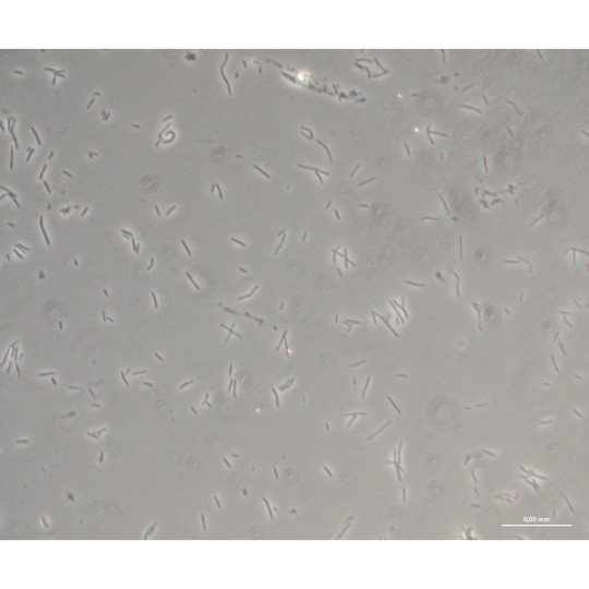
Lactobacillus Casei (friendly bacteria found in dairy products) captured under the microscope using phase contrast microscopy.
#lactobacillus#lactobacillus casei#phase contrast#phase contrast microscopy#microscope#microscopy#science#gut health
20 notes
·
View notes
Text
how to tell if your pot plant will bud?
Cannabis cultivation requires a nuanced understanding of plant physiology, environmental factors, and growth cycles. One of the most critical phases in a cannabis plant’s life cycle is the transition from vegetative growth to flowering (budding). For growers—whether commercial cultivators or home gardeners—accurately identifying pre-flowering signs ensures optimal yield and potency. This 4,000-word guide explores the biological markers, environmental triggers, and cultivation techniques to determine if your cannabis plant is preparing to bud.
1. Understanding Cannabis Growth Stages
To recognize budding readiness, one must first understand the plant’s life cycle. Cannabis progresses through four primary stages:
Germination (5–10 days)
Seedling (2–3 weeks)
Vegetative Growth (3–16 weeks)
Flowering (6–12 weeks).
The shift from vegetative to flowering is triggered by hormonal changes influenced by photoperiodism (light exposure) in photoperiod-dependent strains. Autoflowering varieties, by contrast, transition automatically based on age.
2. Pre-Flowering Indicators: Sex Determination and Early Bud Development
2.1 Sexual Dimorphism in Cannabis
Cannabis is dioecious, meaning plants are either male (produce pollen sacs) or female (develop buds). Hermaphroditic traits may also appear under stress.
Female Pre-Flowers:
Stigma and Pistils: The first sign of female pre-flowers is the emergence of pistils—hair-like structures (white or pink) protruding from small bracts at node junctions.
Calyx Formation: A teardrop-shaped calyx (seed pod) forms at the base of pistils.
Male Pre-Flowers:
Pollen Sacs: Male plants develop clusters of round, grape-like sacs at nodes. These lack pistils and eventually release pollen.
Timing: Pre-flowers typically appear 4–6 weeks into vegetative growth, but environmental stress or genetic factors may accelerate this.
2.2 Structural Changes
Internode Spacing: As flowering approaches, internode gaps shorten, creating denser foliage.
Apical Dominance Shift: The plant redirects energy from vertical growth to lateral branch and bud site development.
3. Environmental Triggers for Flowering
3.1 Photoperiod Manipulation
Photoperiod-sensitive strains (e.g., Indica, Sativa) require specific light schedules to initiate flowering:
Indoor Cultivation: Reduce light exposure from 18–24 hours (vegetative) to 12 hours of light/12 hours of uninterrupted darkness.
Outdoor Cultivation: Flowering begins naturally as daylight hours shorten after the summer solstice.
Light Leaks: Even brief light interruptions during dark periods can disrupt flowering via phytochrome signaling. Use blackout curtains or sealed grow tents.
3.2 Temperature and Humidity
Day/Night Temperature Differential: A 10–15°F (5–8°C) drop at night mimics autumn conditions, stimulating bud development.
Ideal Ranges:
Vegetative: 70–85°F (21–30°C), 40–70% RH
Flowering: 65–80°F (18–26°C), 40–50% RH
High humidity (>60%) in flowering increases mold risk (e.g., botrytis).
3.3 Nutrient Availability
Nitrogen (N) Reduction: During flowering, reduce nitrogen to prevent excessive foliage. Increase phosphorus (P) and potassium (K) for bud formation.
Bloom Boosters: Use fertilizers with NPK ratios like 1-3-2 or 0-5-4.
4. Advanced Diagnostic Tools
4.1 Microscopic Analysis
Trichome Development: Use a 60x–100x jeweler’s loupe to monitor trichomes (resin glands):
Clear: Immature
Cloudy: Peak THC
Amber: Degrading THC to CBN (sedative effects)
4.2 Spectral Sensors
Advanced growers use PAR (Photosynthetically Active Radiation) meters to ensure optimal light intensity (600–900 µmol/m²/s for flowering).
5. Stress-Induced Flowering and Troubleshooting
5.1 Low-Stress Training (LST)
Bending stems to expose bud sites to light can accelerate flowering.
5.2 Common Issues
Light Burn: Bleached buds from excessive intensity.
Nutrient Lockout: Incorrect pH (ideal: 6.0–6.5 for soil, 5.5–6.0 for hydroponics) prevents nutrient uptake.
Hermaphroditism: Caused by light stress, physical damage, or temperature extremes. Remove male flowers immediately.
6. Genetic and Strain-Specific Variations
Indica vs. Sativa: Indica strains flower faster (8–10 weeks) vs. Sativa (10–12 weeks).
Autoflowers: Begin flowering at 2–4 weeks regardless of light cycles.
7. Conclusion: Integrating Science and Observation
Successful cannabis cultivation hinges on synthesizing environmental control, nutritional management, and vigilant observation. By recognizing pre-flowering signs early, growers can optimize conditions for robust bud development, maximizing both yield and cannabinoid content.
Appendices
Glossary of Terms
Recommended pH Adjustment Products
Lighting Schedules by Strain Type
This guide combines botanical science with practical insights, equipping growers to confidently navigate the flowering phase. For further reading, consult peer-reviewed studies in Journal of Cannabis Research or horticultural textbooks such as The Cannabis Grow Bible.
Thump Weed Vertical Grow
https://www.mobilegrowsystem.com
0 notes
Text

Crystallizing time
In their ongoing efforts to push the boundaries of quantum possibilities, physicists in Arts & Sciences at Washington University in St. Louis have created a new type of “time crystal,” a novel phase of matter that defies common perceptions of motion and time.
The WashU research team includes Kater Murch, the Charles M. Hohenberg Professor of Physics, Chong Zu, an assistant professor of physics, and Zu’s graduate students Guanghui He, Ruotian “Reginald” Gong, Changyu Yao, and Zhongyuan Liu. Bingtian Ye from the Massachusetts Institute of Technology and Harvard University’s Norman Yao are also authors of the research, which has been published in the prestigious journal Physical Review X.
Zu, He, and Ye spoke about their achievement and the implications of catching time in a crystal.
What is a time crystal?
To understand a time crystal, it helps to think about familiar crystals such as diamonds or quartz. Those minerals owe their shape and shine to their highly organized structures. The carbon atoms in a diamond interact with each other to form repeated, predictable patterns.
Much like the atoms in a normal crystal repeat patterns in space, the particles in a time crystal repeat patterns over time, Zu explained. In other words, they vibrate or “tick” at constant frequencies, making them crystalized in four dimensions: the three physical dimensions plus the dimension of time.
What makes a time crystal special?
Time crystals are like a clock that never needs winding or batteries. “In theory, it should be able to go on forever,” Zu said. In practice, time crystals are fragile and sensitive to the environment. “We were able to observe hundreds of cycles in our crystals before they broke down, which is impressive.”
Time crystals have been around for a little while; the first one was created at the University of Maryland in 2016. The WashU-led team has gone one step further to build something even more incredible: a time quasicrystal. “It’s an entirely new phase of matter,” Zu said.
How is a time quasicrystal different from a time crystal?
In material science, quasicrystals are recently discovered substances that are highly organized even though their atoms don’t follow the same patterns in every dimension. In the same way, the different dimensions of time quasicrystals vibrate at different frequencies, explained He, the lead author of the paper. The rhythms are very precise and highly organized, but it’s more like a chord than a single note. “We believe we are the first group to create a true time quasicrystal,” He said.
How are time quasicrystals created?
The team built their quasicrystals inside a small, millimeter-sized chunk of diamond. They then bombarded the diamond with beams of nitrogen that were powerful enough to knock out carbon atoms, leaving atom-sized blank spaces. Electrons move into those spaces, and each electron has quantum-level interactions with its neighbors. Zu and colleagues used a similar approach to build a quantum diamond microscope.
The time quasicrystals are made up of more than a million of these vacancies in the diamond. Each quasicrystal is roughly one micrometer (one-thousandth of a millimeter) across, which is too small to be seen without a microscope. “We used microwave pulses to start the rhythms in the time quasicrystals,” Ye said. “The microwaves help create order in time.”
What are the potential uses of time crystals or quasicrystals?
The mere existence of time crystals and quasicrystals confirms some basic theories of quantum mechanics, so they’re useful in that way, Zu said. But they might have practical applications as well. Because they are sensitive to quantum forces such as magnetism, time crystals could be used as long-lasting quantum sensors that never need to be recharged.
Time crystals also offer a novel route to precision timekeeping. Quartz crystal oscillators in watches and electronics tend to drift and require calibration. A time crystal, by contrast, could maintain a consistent tick with minimal loss of energy. A time quasicrystal sensor could potentially measure multiple frequencies at once, creating a fuller picture of the lifetime of a quantum material. First, researchers would need to better understand how to read and track the signal. They can’t yet precisely tell time with a time crystal; they can only make it tick.
Because time crystals can theoretically tick forever without losing energy, there’s a lot of interest in harnessing their power for quantum computers. “They could store quantum memory over long periods of time, essentially like a quantum analog of RAM,” Zu said. “We’re a long way from that sort of technology, but creating a time quasicrystal is a crucial first step.”
IMAGE: WashU physicists shine a microwave laser into a chunk of diamond to create a time quasicrystal, a new phase of matter that repeats precise patterns in time and space. Credit Chong Zu laboratory, Washington University in St. Louis
1 note
·
View note
Text
Physicists magnetize a material with light
New Post has been published on https://sunalei.org/news/physicists-magnetize-a-material-with-light/
Physicists magnetize a material with light

MIT physicists have created a new and long-lasting magnetic state in a material, using only light.
In a study appearing today in Nature, the researchers report using a terahertz laser — a light source that oscillates more than a trillion times per second — to directly stimulate atoms in an antiferromagnetic material. The laser’s oscillations are tuned to the natural vibrations among the material’s atoms, in a way that shifts the balance of atomic spins toward a new magnetic state.
The results provide a new way to control and switch antiferromagnetic materials, which are of interest for their potential to advance information processing and memory chip technology.
In common magnets, known as ferromagnets, the spins of atoms point in the same direction, in a way that the whole can be easily influenced and pulled in the direction of any external magnetic field. In contrast, antiferromagnets are composed of atoms with alternating spins, each pointing in the opposite direction from its neighbor. This up, down, up, down order essentially cancels the spins out, giving antiferromagnets a net zero magnetization that is impervious to any magnetic pull.
If a memory chip could be made from antiferromagnetic material, data could be “written” into microscopic regions of the material, called domains. A certain configuration of spin orientations (for example, up-down) in a given domain would represent the classical bit “0,” and a different configuration (down-up) would mean “1.” Data written on such a chip would be robust against outside magnetic influence.
For this and other reasons, scientists believe antiferromagnetic materials could be a more robust alternative to existing magnetic-based storage technologies. A major hurdle, however, has been in how to control antiferromagnets in a way that reliably switches the material from one magnetic state to another.
“Antiferromagnetic materials are robust and not influenced by unwanted stray magnetic fields,” says Nuh Gedik, the Donner Professor of Physics at MIT. “However, this robustness is a double-edged sword; their insensitivity to weak magnetic fields makes these materials difficult to control.”
Using carefully tuned terahertz light, the MIT team was able to controllably switch an antiferromagnet to a new magnetic state. Antiferromagnets could be incorporated into future memory chips that store and process more data while using less energy and taking up a fraction of the space of existing devices, owing to the stability of magnetic domains.
“Generally, such antiferromagnetic materials are not easy to control,” Gedik says. “Now we have some knobs to be able to tune and tweak them.”
Gedik is the senior author of the new study, which also includes MIT co-authors Batyr Ilyas, Tianchuang Luo, Alexander von Hoegen, Zhuquan Zhang, and Keith Nelson, along with collaborators at the Max Planck Institute for the Structure and Dynamics of Matter in Germany, University of the Basque Country in Spain, Seoul National University, and the Flatiron Institute in New York.
Off balance
Gedik’s group at MIT develops techniques to manipulate quantum materials in which interactions among atoms can give rise to exotic phenomena.
“In general, we excite materials with light to learn more about what holds them together fundamentally,” Gedik says. “For instance, why is this material an antiferromagnet, and is there a way to perturb microscopic interactions such that it turns into a ferromagnet?”
In their new study, the team worked with FePS3 — a material that transitions to an antiferromagnetic phase at a critical temperature of around 118 kelvins (-247 degrees Fahrenheit).
The team suspected they might control the material’s transition by tuning into its atomic vibrations.
“In any solid, you can picture it as different atoms that are periodically arranged, and between atoms are tiny springs,” von Hoegen explains. “If you were to pull one atom, it would vibrate at a characteristic frequency which typically occurs in the terahertz range.”
The way in which atoms vibrate also relates to how their spins interact with each other. The team reasoned that if they could stimulate the atoms with a terahertz source that oscillates at the same frequency as the atoms’ collective vibrations, called phonons, the effect could also nudge the atoms’ spins out of their perfectly balanced, magnetically alternating alignment. Once knocked out of balance, atoms should have larger spins in one direction than the other, creating a preferred orientation that would shift the inherently nonmagnetized material into a new magnetic state with finite magnetization.
“The idea is that you can kill two birds with one stone: You excite the atoms’ terahertz vibrations, which also couples to the spins,” Gedik says.
Shake and write
To test this idea, the team worked with a sample of FePS3 that was synthesized by colleages at Seoul National University. They placed the sample in a vacuum chamber and cooled it down to temperatures at and below 118 K. They then generated a terahertz pulse by aiming a beam of near-infrared light through an organic crystal, which transformed the light into the terahertz frequencies. They then directed this terahertz light toward the sample.
“This terahertz pulse is what we use to create a change in the sample,” Luo says. “It’s like ‘writing’ a new state into the sample.”
To confirm that the pulse triggered a change in the material’s magnetism, the team also aimed two near-infrared lasers at the sample, each with an opposite circular polarization. If the terahertz pulse had no effect, the researchers should see no difference in the intensity of the transmitted infrared lasers.
“Just seeing a difference tells us the material is no longer the original antiferromagnet, and that we are inducing a new magnetic state, by essentially using terahertz light to shake the atoms,” Ilyas says.
Over repeated experiments, the team observed that a terahertz pulse successfully switched the previously antiferromagnetic material to a new magnetic state — a transition that persisted for a surprisingly long time, over several milliseconds, even after the laser was turned off.
“People have seen these light-induced phase transitions before in other systems, but typically they live for very short times on the order of a picosecond, which is a trillionth of a second,” Gedik says.
In just a few milliseconds, scientists now might have a decent window of time during which they could probe the properties of the temporary new state before it settles back into its inherent antiferromagnetism. Then, they might be able to identify new knobs to tweak antiferromagnets and optimize their use in next-generation memory storage technologies.
This research was supported, in part, by the U.S. Department of Energy, Materials Science and Engineering Division, Office of Basic Energy Sciences, and the Gordon and Betty Moore Foundation.
0 notes
Text
Physicists magnetize a material with light
New Post has been published on https://thedigitalinsider.com/physicists-magnetize-a-material-with-light/
Physicists magnetize a material with light

MIT physicists have created a new and long-lasting magnetic state in a material, using only light.
In a study appearing today in Nature, the researchers report using a terahertz laser — a light source that oscillates more than a trillion times per second — to directly stimulate atoms in an antiferromagnetic material. The laser’s oscillations are tuned to the natural vibrations among the material’s atoms, in a way that shifts the balance of atomic spins toward a new magnetic state.
The results provide a new way to control and switch antiferromagnetic materials, which are of interest for their potential to advance information processing and memory chip technology.
In common magnets, known as ferromagnets, the spins of atoms point in the same direction, in a way that the whole can be easily influenced and pulled in the direction of any external magnetic field. In contrast, antiferromagnets are composed of atoms with alternating spins, each pointing in the opposite direction from its neighbor. This up, down, up, down order essentially cancels the spins out, giving antiferromagnets a net zero magnetization that is impervious to any magnetic pull.
If a memory chip could be made from antiferromagnetic material, data could be “written” into microscopic regions of the material, called domains. A certain configuration of spin orientations (for example, up-down) in a given domain would represent the classical bit “0,” and a different configuration (down-up) would mean “1.” Data written on such a chip would be robust against outside magnetic influence.
For this and other reasons, scientists believe antiferromagnetic materials could be a more robust alternative to existing magnetic-based storage technologies. A major hurdle, however, has been in how to control antiferromagnets in a way that reliably switches the material from one magnetic state to another.
“Antiferromagnetic materials are robust and not influenced by unwanted stray magnetic fields,” says Nuh Gedik, the Donner Professor of Physics at MIT. “However, this robustness is a double-edged sword; their insensitivity to weak magnetic fields makes these materials difficult to control.”
Using carefully tuned terahertz light, the MIT team was able to controllably switch an antiferromagnet to a new magnetic state. Antiferromagnets could be incorporated into future memory chips that store and process more data while using less energy and taking up a fraction of the space of existing devices, owing to the stability of magnetic domains.
“Generally, such antiferromagnetic materials are not easy to control,” Gedik says. “Now we have some knobs to be able to tune and tweak them.”
Gedik is the senior author of the new study, which also includes MIT co-authors Batyr Ilyas, Tianchuang Luo, Alexander von Hoegen, Zhuquan Zhang, and Keith Nelson, along with collaborators at the Max Planck Institute for the Structure and Dynamics of Matter in Germany, University of the Basque Country in Spain, Seoul National University, and the Flatiron Institute in New York.
Off balance
Gedik’s group at MIT develops techniques to manipulate quantum materials in which interactions among atoms can give rise to exotic phenomena.
“In general, we excite materials with light to learn more about what holds them together fundamentally,” Gedik says. “For instance, why is this material an antiferromagnet, and is there a way to perturb microscopic interactions such that it turns into a ferromagnet?”
In their new study, the team worked with FePS3 — a material that transitions to an antiferromagnetic phase at a critical temperature of around 118 kelvins (-247 degrees Fahrenheit).
The team suspected they might control the material’s transition by tuning into its atomic vibrations.
“In any solid, you can picture it as different atoms that are periodically arranged, and between atoms are tiny springs,” von Hoegen explains. “If you were to pull one atom, it would vibrate at a characteristic frequency which typically occurs in the terahertz range.”
The way in which atoms vibrate also relates to how their spins interact with each other. The team reasoned that if they could stimulate the atoms with a terahertz source that oscillates at the same frequency as the atoms’ collective vibrations, called phonons, the effect could also nudge the atoms’ spins out of their perfectly balanced, magnetically alternating alignment. Once knocked out of balance, atoms should have larger spins in one direction than the other, creating a preferred orientation that would shift the inherently nonmagnetized material into a new magnetic state with finite magnetization.
“The idea is that you can kill two birds with one stone: You excite the atoms’ terahertz vibrations, which also couples to the spins,” Gedik says.
Shake and write
To test this idea, the team worked with a sample of FePS3 that was synthesized by colleages at Seoul National University. They placed the sample in a vacuum chamber and cooled it down to temperatures at and below 118 K. They then generated a terahertz pulse by aiming a beam of near-infrared light through an organic crystal, which transformed the light into the terahertz frequencies. They then directed this terahertz light toward the sample.
“This terahertz pulse is what we use to create a change in the sample,” Luo says. “It’s like ‘writing’ a new state into the sample.”
To confirm that the pulse triggered a change in the material’s magnetism, the team also aimed two near-infrared lasers at the sample, each with an opposite circular polarization. If the terahertz pulse had no effect, the researchers should see no difference in the intensity of the transmitted infrared lasers.
“Just seeing a difference tells us the material is no longer the original antiferromagnet, and that we are inducing a new magnetic state, by essentially using terahertz light to shake the atoms,” Ilyas says.
Over repeated experiments, the team observed that a terahertz pulse successfully switched the previously antiferromagnetic material to a new magnetic state — a transition that persisted for a surprisingly long time, over several milliseconds, even after the laser was turned off.
“People have seen these light-induced phase transitions before in other systems, but typically they live for very short times on the order of a picosecond, which is a trillionth of a second,” Gedik says.
In just a few milliseconds, scientists now might have a decent window of time during which they could probe the properties of the temporary new state before it settles back into its inherent antiferromagnetism. Then, they might be able to identify new knobs to tweak antiferromagnets and optimize their use in next-generation memory storage technologies.
This research was supported, in part, by the U.S. Department of Energy, Materials Science and Engineering Division, Office of Basic Energy Sciences, and the Gordon and Betty Moore Foundation.
#antiferromagnets#atom#atomic#atoms#author#beam#birds#change#chip#chips#classical#Collective#crystal#data#devices#direction#domains#double#dynamics#easy#Electronics#energy#engineering#Foundation#Fraction#Future#Germany#Giving#how#how to
0 notes