#Scanning Tunneling Microscopy
Explore tagged Tumblr posts
Visit Tumblr Blog
Explore Tumblr blogs with no restrictions, modern design and the best experience.
Last Seen Tumblr Blogs


Fun Fact
Tumblr’s website traffic is steadily declining.
Text

Physicists take a step closer to controlling single-molecule chemical reactions
Controlling matter at the atomic level has taken a major step forward, thanks to nanotechnology research by an international team of scientists led by physicists at the University of Bath. This advancement has profound implications for fundamental scientific understanding. It is also likely to have important practical applications, such as transforming the way researchers develop new medications. Controlling single-outcome single-molecule reactions is now almost routine in research laboratories across the world. For example, more than a decade ago, researchers from the technology giant IBM showcased their ability to manipulate individual atoms by creating "A boy and his atom," the world's smallest movie. In the film, single molecules, consisting of two atoms bonded together, were magnified 100-million times and positioned frame-by-frame to tell a stop-motion story on an atomic scale.
Read more.
#Materials Science#Science#Reactions#Molecules#Chemistry#Scanning tunneling microscopy#University of Bath
16 notes
·
View notes
Note
Do you have any formal published work for your OC's? Like is there a comic somewhere or some fics? I'd really love to learn more about the narrative, the characters are gorgeous 🎀
there is not _(:3」∠)_
but I've tried! i've honest to god written all the issues of a would-be transient comic and thumbnailed/storyboarded several of them out, but when i went to actually make them proper, it was too much to do on top of my job/other interests. plus I just...didnt like them. i couldnt settle on a consistent style and the rendering type i chose both looked overwhelming and took too much time.
for an example of what i meant, heres two example pages from my last attempt.


The thing is if i never actually make the comic, then in my head it can be the coolest, raddest, thing ever, but once pen meets paper the hypothetical has to clash with the reality that its not going to be as funny or polished as i dreamt it'd be. but ive been building up more illustrative art confidence and solved some of the problems i had on that above attempt (not understanding the style i want, rendering woes) so ??? ?????? who knows.
of all the OCverses, transient is the most actionable since 1) its fully written. like im literally looking at the full script right now. i just need to do it. and 2) its inherently episodic so i could publish issue-by-issue without having to commit to some ~50 cohesive, continuous chapters that would be needed for something like stitch in the ditch.
but thank you!!!! i would like to make it someday but its a matter of getting the mind and body to be fully willing lol.
#my favorite one i wrote was called STM: shrimp time motherfucker#which is a play on my job STM or scanning tunneling microscopy#instead of tunneling electrons across a tip and sample- shrimp were quantum tunneling into places they're classically forbidden to be#which was intended to teach about first principles of QM and tunneling across finite barriers
14 notes
·
View notes
Text

A Fourier transform of an image obtained using scanning tunneling microscopy of electrons on the surface of a crystal of zirconium silicon sulfide, showing the symmetry of the electron system. Reproduced from Ref. 1 and licensed under CC BY 4.0. @ 2025 C. J. Butler et al.
https://www.nanotechnologyworld.org/post/spontaneous-symmetry-breaking-in-electron-systems-proves-elusive
7 notes
·
View notes
Note
What do you have the male/male cables in the lab for?
a method of electron microscopy we do in the lab is called STM, or scanning tunneling microscope. STMs involve electrons quantum tunneling between an atomically sharp tip and a sample of interest. The flow of hopping electrons, ie the magnitude of the tunneling current, is later interpreted as an atomic image. This is a useful technique for understanding the surface structure and electrical properties of materials.
thats all fine and dandy but to get true atomic resolution, you need an insanely sharp tip since you want the electrons to tunnel around as small of a point as possible. Theres a number of ways to do this, however one of the methods we used for a long time was well........We'd have some very fine tungsten wire. we hook the wire up to one end of the widow maker (ie the male/male cable) that's plugged into an AC power supply, and hook the other end around a little gold hoop...and then they both get submerged into KOH, which is highly corrosive and has a ph anywhere from 10-13. we let them sit in the corrosive base for a small period of time until the base and the AC current cause the tungsten wire to etch away and eventually break off at the surface, which generates a very fine, precise tip point that can be used for imaging.
so dont worry folks, not only am i working with male/male cables that are open and supplied with an active AC current, we're also putting that current through a liquid corrosive enough to immediately burn your skin on contact.
#in case youre wondering there are a million safer ways to do this#our PI just loves hunting us for sport#between making us work on a live 20k powerbox and running 35 amps of current through open wires
37 notes
·
View notes
Text
The Revolutionary History of Nanotechnology

Nanotechnology, a groundbreaking field that has revolutionized numerous industries, continues to shape the world as we know it. In this article, we delve into the rich history of nanotechnology, exploring its origins, major milestones, and transformative applications. Join us on this captivating journey through the nano realm and discover how this remarkable technology has reshaped various sectors, from healthcare and electronics to energy and materials science.
Origins of Nanotechnology
Unveiling the Nanoscale
Nanotechnology finds its roots in the exploration of the minuscule world at the nanoscale. The concept of nanoscale was first introduced by physicist Richard Feynman in his visionary lecture in 1959, where he discussed the potential for manipulating matter at the atomic and molecular levels. This groundbreaking concept laid the foundation for the birth of nanotechnology.
The Birth of Nanotechnology
In 1981, the term "nanotechnology" was officially coined by engineer K. Eric Drexler in his influential book, "Engines of Creation." Drexler envisioned a future where nanomachines could manipulate matter at the atomic scale, leading to remarkable advancements in various fields. His work served as a catalyst for the rapid development of nanotechnology research and applications.

Major Milestones in Nanotechnology
Scanning Probe Microscopy
In the early 1980s, the invention of scanning probe microscopy revolutionized nanotechnology research. The scanning tunneling microscope (STM) and atomic force microscope (AFM) allowed scientists to visualize and manipulate individual atoms and molecules with unprecedented precision. These breakthroughs opened up new possibilities for studying nanoscale phenomena and laid the groundwork for further advancements in the field.
Fullerenes and Nanotubes
In 1985, a significant discovery shook the scientific community—the identification of fullerenes. Researchers Robert Curl, Harold Kroto, and Richard Smalley stumbled upon these unique carbon molecules, marking the birth of a new class of nanomaterials. Fullerenes paved the way for the development of carbon nanotubes, cylindrical structures with remarkable strength and conductivity. These nanotubes would go on to become key building blocks in various nanotechnology applications.
Nanotechnology in Medicine
Nanotechnology's potential to revolutionize healthcare became evident with the advent of targeted drug delivery systems. Nanoparticles, such as liposomes and polymeric nanoparticles, can be designed to encapsulate drugs and deliver them precisely to targeted cells or tissues. This approach minimizes side effects and maximizes therapeutic efficacy. Additionally, nanotechnology plays a vital role in imaging techniques, enabling highly sensitive and precise detection of diseases at the molecular level.
Nanoelectronics and Quantum Computing
The relentless pursuit of smaller, faster, and more energy-efficient electronics led to the emergence of nanoelectronics. By utilizing nanoscale materials and devices, researchers have pushed the boundaries of traditional silicon-based technology. Nanoscale transistors, quantum dots, and nanowires have paved the way for advancements in computing power, memory storage, and energy efficiency. Furthermore, the field of quantum computing, which harnesses quantum phenomena at the nanoscale, holds the promise of solving complex problems that are currently beyond the capabilities of classical computers.
Nanomaterials and Energy
Nanotechnology has also played a significant role in addressing global energy challenges. By developing advanced nanomaterials, scientists have made strides in enhancing solar cell efficiency, enabling the production of clean and renewable energy. Nanomaterials have also been employed in energy storage devices, such as batteries and supercapacitors, to improve their performance and longevity. Additionally, nanotechnology has opened up avenues for energy harvesting and energy conversion, contributing to a more sustainable future.

Transformative Applications of Nanotechnology
Nanomedicine and Disease Treatment
Nanotechnology has revolutionized medicine, offering innovative solutions for disease diagnosis, treatment, and prevention. Targeted drug delivery systems, nanoscale imaging techniques, and nanobiosensors have transformed the landscape of healthcare, enabling personalized and precise interventions. From cancer therapy to regenerative medicine, nanotechnology has the potential to revolutionize patient care and improve outcomes.
Nanoelectronics and Wearable Technology
The marriage of nanotechnology and electronics has given rise to the era of wearable technology. Nanoscale sensors, flexible displays, and energy-efficient components have paved the way for smartwatches, fitness trackers, and augmented reality devices. These advancements in nanoelectronics have made it possible to integrate technology seamlessly into our everyday lives, enhancing convenience and connectivity.
Nanomaterials and Advanced Manufacturing
Nanotechnology has propelled advancements in materials science and manufacturing. Nanomaterials with tailored properties and enhanced performance characteristics have found applications in aerospace, automotive, and construction industries. From lightweight and high-strength composites to self-cleaning surfaces and energy-efficient coatings, nanomaterials have revolutionized product design, durability, and sustainability.
In Conclusion
Nanotechnology's journey from its conceptualization to its present-day applications has been nothing short of extraordinary. The field's remarkable achievements in diverse domains, including medicine, electronics, and energy, continue to drive innovation and shape the future. As we delve deeper into the nanoscale world, the possibilities seem boundless. With ongoing research and collaboration, nanotechnology will undoubtedly unlock new frontiers, leading to breakthroughs that will reshape industries and improve lives across the globe.
#history of nanotechnology#richard feynman#chemestry#green chemistry#nanotechnology#science#nanomaterials#nanocoating#nanomedicine#probe microscopy#revolutionary
3 notes
·
View notes
Text
Postdoctoral Research Associate- Thin Film Synthesis and Characterization of Quantum Materials
Job title: Postdoctoral Research Associate- Thin Film Synthesis and Characterization of Quantum Materials Company: Oak Ridge National Laboratory Job description: , you will focus on the growth of thin film and heterostructure quantum materials utilizing molecular beam epitaxy, and probing the… thin film synthesis, ultrahigh vacuum techniques such as scanning tunneling microscopy and…
0 notes
Text
2412.18332v1
저자: PyAtoms: An interactive tool for rapidly simulating atomic scanning tunneling microscopy images of 2D materials, moir´e systems and superlattices C. Guti´errez and A. G. Prado Department of Physics and Astronomy, University of California, Los Angeles, Los Angeles, California, 90095 USA E-mail: [email protected] Abstract. We present PyAtoms, an interactive open-source software that…
0 notes
Text
Innovations and Techniques in Analytical Sciences
Analytical sciences are constantly evolving, driven by the need for more precise, efficient, and cost-effective methods to analyze and characterize substances across various industries. From pharmaceuticals to environmental monitoring, innovations in analytical techniques have revolutionized the way we understand materials, chemicals, and biological systems. This article explores the latest advancements in analytical sciences, highlighting innovative techniques that are shaping the future of research, development, and quality control.
The Growing Importance of Analytical Sciences
Analytical sciences are pivotal in multiple sectors, from healthcare to manufacturing, as they provide the tools to measure, identify, and analyze chemical compositions with remarkable precision. With the increasing complexity of research and industry needs, analytical methods must continuously adapt to address challenges such as real-time monitoring, data volume, and miniaturization of tools for portable applications.
Recent breakthroughs in analytical techniques promise to enhance the speed, accuracy, and reliability of scientific discoveries, impacting everything from drug development to environmental conservation. Let’s explore some of the key innovations and cutting-edge techniques in analytical sciences.

Innovations in Analytical Techniques
1. High-Resolution Mass Spectrometry (HRMS)
Mass spectrometry (MS) is already a cornerstone of analytical chemistry, but high-resolution mass spectrometry (HRMS) has taken this technique to new heights. HRMS allows for the detection and characterization of ions with unparalleled accuracy and resolution, making it indispensable in complex molecular analyses, such as proteomics, metabolomics, and drug testing.
Benefits:
Enhanced sensitivity for detecting low-abundance compounds.
High resolution allows for the identification of structural isomers with minimal interference.
Essential for analyzing complex mixtures in pharmaceuticals and environmental testing.
2. Raman Spectroscopy for Real-Time Analysis
Raman spectroscopy is a non-destructive technique that provides rapid, real-time analysis of molecular structures. Recent advancements in Raman spectrometers have made them more portable and accessible for in-field applications. This innovation is crucial in industries like pharmaceuticals, food safety, and environmental monitoring, where timely data is essential.
Applications:
Pharmaceuticals: Verifying the chemical composition of drugs in real time during production.
Food: Detecting contaminants or adulterants without the need for complex sample preparation.
Environmental Science: Monitoring air and water quality by analyzing molecular fingerprints of pollutants.
3. Nano-Analytical Tools
Nanotechnology is expanding the boundaries of analytical sciences by providing tools that can analyze materials at the molecular and atomic scale. Techniques such as atomic force microscopy (AFM) and scanning tunneling microscopy (STM) allow scientists to directly observe surfaces, structures, and even individual atoms with incredible precision.
Benefits:
Detailed imaging and analysis of nanoparticles, which are essential in drug delivery and materials science.
Understanding surface properties at the atomic level, crucial for designing new materials and enhancing the performance of electronic devices.
Unlocking new possibilities in biomolecular research, including protein folding and molecular interactions.
4. Integration of Artificial Intelligence (AI) and Machine Learning (ML)
The integration of AI and machine learning (ML) in analytical sciences has opened new frontiers in data interpretation and analysis. With the ability to process vast datasets and recognize complex patterns, AI-driven approaches significantly improve the accuracy and efficiency of analytical techniques.
Applications:
Pharmaceuticals: Predicting drug interactions and identifying potential drug candidates using large chemical datasets.
Environmental Monitoring: Analyzing environmental data to detect subtle patterns in air and water quality that may indicate emerging risks.
Manufacturing: Predicting material failure or optimizing production processes based on data analytics.
AI and ML algorithms can also aid in automating tedious and repetitive tasks, reducing human error and speeding up analytical workflows.
5. Portable Analytical Devices
One of the most transformative innovations in analytical sciences is the development of portable devices that allow for in-field analysis. These handheld instruments are compact, easy to use, and capable of providing real-time results, making them invaluable in environmental, forensic, and pharmaceutical applications.
Examples:
Portable Raman Spectrometers: For field-based chemical analysis, especially in remote areas.
Handheld X-ray Fluorescence (XRF) Spectrometers: Used in geological surveys and material science to analyze elemental composition on-site.
Portable DNA Analyzers: For quick genetic analysis in medical diagnostics or wildlife research.
These devices enable researchers and professionals to make critical decisions without the need for laboratory settings, improving the speed and efficiency of data collection.
Future Trends in Analytical Sciences
1. Sustainability in Analytical Chemistry
As environmental concerns grow, the need for sustainable analytical practices has become more pressing. Innovations in green chemistry and eco-friendly analytical methods are now taking center stage. Techniques such as green solvents, energy-efficient instruments, and non-toxic reagents are increasingly being incorporated into laboratory practices to reduce waste and energy consumption.
Green Analytical Chemistry: Emphasizes the use of renewable materials and eco-friendly methodologies, helping to minimize environmental impact while maintaining analytical precision.
2. Miniaturization and Lab-on-a-Chip
The miniaturization of analytical instruments, especially in the form of lab-on-a-chip devices, promises to revolutionize fields like medical diagnostics and environmental monitoring. These micro-scale devices integrate multiple analytical functions on a single chip, making them portable, affordable, and capable of performing complex analyses quickly.
Applications:
Medical Diagnostics: Rapid point-of-care testing for disease markers and pathogens.
Environmental Monitoring: Real-time pollution detection and analysis in air and water systems.
3. 3D Imaging and Spectroscopy
3D imaging techniques are gaining popularity in analytical sciences, particularly in material science and biology. These methods, including 3D electron microscopy and 3D Raman spectroscopy, enable researchers to study samples in three dimensions, providing more detailed and accurate insights into structures at the molecular level.
Applications:
Drug Development: Mapping the structure of biological targets and evaluating how drug molecules interact with them.
Material Science: Investigating the properties of complex materials and composites in 3D, leading to better product designs.
Conclusion
Innovations in analytical sciences are continuously pushing the boundaries of what is possible in research and industry. From high-resolution mass spectrometry to AI-driven analysis, these advancements are revolutionizing how we approach complex scientific challenges. With growing demand for precision, efficiency, and sustainability, the future of analytical sciences promises even more transformative techniques and applications across diverse fields, including pharmaceuticals, environmental monitoring, and materials science. The ongoing developments in this field are not just improving existing processes but also creating new possibilities for scientific discovery and innovation.
1 note
·
View note
Text
Microscopy Market: Illuminating the Future of Research
The Microscopy market is pivotal in advancing scientific research and medical diagnostics by providing detailed and precise imaging of samples at microscopic levels. As technology evolves and research demands increase, the microscopy market is expanding rapidly. This article explores the latest trends, market segmentation, key growth drivers, and leading companies in the microscopy industry.
Market Overview
According to SkyQuest’s Microscopy Market report, the global microscopy market is valued at USD 7.2 billion in 2023, with a projected CAGR of 5.8% during the forecast period. The market growth is driven by technological advancements in microscopy techniques, increasing research activities, and the rising demand for detailed imaging in medical diagnostics.
Request Your Free Sample: - https://www.skyquestt.com/sample-request/microscopy-market
Market Segmentation
By Type:
Optical Microscopes: Includes light microscopes such as brightfield, darkfield, and fluorescence microscopes for various imaging needs.
Electron Microscopes: Includes scanning electron microscopes (SEM) and transmission electron microscopes (TEM) for high-resolution imaging at the nanometer scale.
Scanning Probe Microscopes: Includes atomic force microscopes (AFM) and scanning tunneling microscopes (STM) for surface characterization at the atomic level.
Others: Includes specialized microscopy techniques like confocal and multiphoton microscopy.
By Application:
Biomedical Research: Essential for studying cellular and molecular structures, disease mechanisms, and drug development.
Material Science: Used for analyzing the structure and properties of materials at microscopic levels.
Semiconductor Industry: Critical for inspecting and analyzing semiconductor materials and devices.
Pharmaceuticals: Supports drug discovery and development through detailed imaging of biological samples.
Others: Includes applications in environmental science, forensics, and education.
By End-User:
Research Laboratories: Major users of advanced microscopy techniques for scientific investigations.
Healthcare and Clinical Laboratories: Utilize microscopy for diagnostic purposes and disease research.
Academic Institutions: Engage in fundamental research and educational activities involving microscopy.
Industrial Sector: Applies microscopy for quality control, material analysis, and product development.
Read More at: - https://www.skyquestt.com/report/microscopy-market
Key Growth Drivers
Technological Advancements: Innovations such as super-resolution microscopy and digital imaging are enhancing microscopy capabilities and driving market growth.
Increasing Research and Development Activities: The expansion of research activities across various fields, including biology and material science, fuels the demand for advanced microscopy solutions.
Rising Demand in Medical Diagnostics: The need for precise imaging in diagnostics, particularly in cancer and neurological diseases, is increasing the adoption of advanced microscopy techniques.
Growth in Nanotechnology: Advances in nanotechnology require sophisticated microscopy tools to observe and manipulate materials at the nanoscale.
Leading Companies in the Market
SkyQuest’s report highlights key players in the Microscopy market, including:
Nikon Corporation
Olympus Corporation
Leica Microsystems
Carl Zeiss AG
Hitachi High-Technologies Corporation
Bruker Corporation
JEOL Ltd.
Thermo Fisher Scientific Inc.
Keyence Corporation
FEI Company
Take Action Now: Secure Your Report Today - https://www.skyquestt.com/buy-now/microscopy-market
Challenges and Opportunities
The microscopy market faces challenges such as high equipment costs and the need for specialized training. However, opportunities exist in developing affordable solutions, expanding applications in emerging fields like nanotechnology, and integrating AI for enhanced image analysis.
Future Outlook
The microscopy market is set for strong growth driven by continuous technological advancements and increasing research needs. Companies that innovate with new microscopy technologies and focus on expanding their applications will be well-positioned to lead the market. For comprehensive insights and strategic recommendations, consult SkyQuest’s Microscopy Market report.
The Microscopy market is crucial for advancing research and medical diagnostics by providing detailed imaging at microscopic levels. As technology progresses and research demands evolve, microscopy will play an increasingly significant role in various fields. Decision-makers in research and healthcare should leverage the latest advancements to stay competitive in this dynamic market. For more in-depth analysis, refer to SkyQuest’s comprehensive Microscopy Market report.
0 notes
Text
Exploring Careers: Jobs in Nanotechnology

Nanotechnology might sound like something out of a sci-fi novel, but it’s very much a part of our present and shaping our future. Whether you’re fascinated by the minute scale of atoms and molecules or you’re excited about revolutionary applications in medicine, energy, and electronics, a career in nanotechnology can be incredibly rewarding. In this guide, we’ll explore the vibrant world of nanotechnology careers, breaking down everything you need to know to get started and thrive in this cutting-edge field.
Understanding Nanotechnology
Definition and Scope
At its core, nanotechnology involves manipulating matter at an incredibly small scale—typically at the level of atoms and molecules. This means working with materials at dimensions between 1 and 100 nanometers. To put that in perspective, a nanometer is one-billionth of a meter. Nanotechnology encompasses various scientific disciplines, including physics, chemistry, materials science, and biology, all converging to create new tools, materials, and technologies.
Historically, the concept of nanotechnology was popularized by physicist Richard Feynman in the 1950s. However, it wasn’t until the 1980s, with the advent of scanning tunneling microscopy and other advanced techniques, that the field began to take shape. Today, nanotechnology is a rapidly evolving field with applications across numerous industries, from healthcare and electronics to energy and environmental science.
Applications of Nanotechnology
Nanotechnology’s versatility is evident in its wide array of applications:
Healthcare: Nanotechnology is revolutionizing medicine with advancements in drug delivery systems, targeted therapies, and diagnostic tools. For instance, nanoparticles can be engineered to deliver drugs directly to cancer cells, minimizing side effects and improving treatment efficacy.
Electronics: In the realm of electronics, nanotechnology enables the creation of smaller, faster, and more efficient devices. Nanomaterials like carbon nanotubes and graphene are pushing the boundaries of electronics, leading to innovations such as flexible displays and ultra-fast transistors.
Energy: Nanotechnology is also playing a critical role in energy. From enhancing the efficiency of solar panels to improving battery performance and developing new methods for energy storage, the field is making significant strides in creating sustainable energy solutions.
Environmental Protection: Nanotechnology offers promising solutions for environmental challenges, including pollution control and waste management. Nanomaterials can help remove contaminants from water and soil or capture harmful gases from the atmosphere.
Educational Pathways and Qualifications
Academic Requirements
If you’re considering a career in nanotechnology, a solid educational foundation is essential. Most roles in this field require a background in science or engineering. Typically, you’ll need at least a bachelor’s degree in a relevant field such as physics, chemistry, materials science, or engineering.
Pursuing advanced degrees like a master’s or PhD can open doors to more specialized roles and research opportunities. These programs often involve a combination of coursework and hands-on research, allowing you to dive deep into nanotechnology and its applications.
Skills and Competencies
To excel in nanotechnology, you’ll need a blend of technical and soft skills:
Technical Skills: Familiarity with nanofabrication techniques, microscopy methods (like scanning electron microscopy), and computational modeling is crucial. These skills enable you to manipulate materials at the nanoscale and analyze their properties.
Soft Skills: Beyond technical know-how, problem-solving, critical thinking, and teamwork are vital. Nanotechnology projects often involve interdisciplinary collaboration, so being able to work effectively with others and approach problems from various angles is important.
Certifications and Training
While formal education provides the foundation, additional certifications and specialized training can enhance your qualifications. Look for certifications in areas like nanofabrication or nanomaterials, and consider attending workshops and seminars to stay updated on the latest developments in the field.
Career Opportunities in Nanotechnology
Research and Development
Research and Development (R&D) roles are at the heart of nanotechnology innovation. As a research scientist or R&D engineer, you’ll be involved in designing experiments, developing new materials, and testing applications. This role often requires a deep understanding of both theoretical concepts and practical techniques.
Industry Roles
Nanotechnology is applied across various industries, leading to diverse career opportunities. In the pharmaceutical industry, for example, you might work as a product development specialist, developing new drug delivery systems. In electronics, you could be involved in improving the performance of nano-enabled devices as a quality control analyst or a product engineer.
Academic and Government Positions
Academia and government institutions offer opportunities for those interested in research and teaching. Positions such as university professor or research coordinator allow you to contribute to the field through teaching and conducting research. These roles often involve securing research grants and publishing findings in scientific journals.
Entrepreneurship and Startups
If you’re entrepreneurial, nanotechnology offers exciting opportunities to start your own business. Entrepreneurs in nanotechnology may focus on creating innovative products or services based on nanoscale materials and techniques. This path requires not only technical expertise but also business acumen and the ability to navigate the startup landscape.
Notable Employers and Organizations
Leading Companies
Numerous companies are at the forefront of nanotechnology, driving innovation across various sectors. These organizations work on everything from advanced materials to new medical technologies. Joining such companies can provide you with hands-on experience and opportunities to work on cutting-edge projects.
Research Institutions
Research institutions are pivotal in advancing nanotechnology. These institutions conduct fundamental research, develop new technologies, and collaborate with industry partners. Working at a research institution can offer a collaborative environment where you can contribute to groundbreaking discoveries.
Government and Non-Profit Organizations
Government agencies and non-profit organizations play a crucial role in supporting nanotechnology research through funding and policy-making. These entities often work on large-scale projects and initiatives aimed at addressing global challenges using nanotechnology.
Trends and Future Directions
Emerging Technologies
The field of nanotechnology is constantly evolving, with new technologies emerging all the time. Advances in areas like quantum dots, nanomedicine, and nanoelectronics are pushing the boundaries of what’s possible. Staying informed about these trends can help you position yourself at the forefront of the industry.
Impact of Nanotechnology on Society
Nanotechnology has the potential to address many societal challenges, from improving healthcare outcomes to creating more sustainable energy solutions. However, it also raises ethical and environmental questions that need to be addressed. Being aware of these issues and engaging in discussions about responsible development is important for anyone in the field.
Predictions for Career Growth
The demand for nanotechnology professionals is expected to grow as the field continues to expand. With applications in diverse industries and ongoing research, there are ample opportunities for those with the right skills and qualifications. Keeping up with industry developments and continuously improving your expertise will be key to advancing your career.
Real-Life Success Stories
Interviews with Professionals
Speaking with professionals currently working in nanotechnology can provide valuable insights into the field. These conversations can reveal the day-to-day responsibilities, challenges, and rewards of working in nanotechnology. Engaging with these individuals through networking events or informational interviews can offer a clearer picture of what to expect.
Case Studies
Case studies of successful projects can illustrate the real-world impact of nanotechnology. Whether it’s a breakthrough in cancer treatment or a new type of nano-enabled sensor, these examples showcase the transformative potential of the field. Learning from these successes can inspire and guide your own career path.
How to Get Started in Nanotechnology
Educational Pathways
To embark on a career in nanotechnology, start by pursuing relevant educational programs. Look for courses and degrees that offer a strong foundation in nanoscience and engineering. Engage in research opportunities during your studies to gain hands-on experience.
Networking and Professional Development
Networking is crucial in nanotechnology, as it allows you to connect with professionals, stay informed about industry trends, and discover job opportunities. Attend conferences, workshops, and join professional organizations related to nanotechnology to expand your network and enhance your knowledge.
Job Search Strategies
When searching for jobs in nanotechnology, tailor your resume to highlight relevant skills and experiences. Seek internships or entry-level positions that provide practical experience in the field. Utilize online job boards, company websites, and professional networks to find opportunities that match your interests and qualifications.
Nanotechnology is a field full of possibilities, offering exciting career opportunities across various sectors. By understanding the scope of nanotechnology, pursuing the right education and skills, and staying informed about industry trends, you can position yourself for a successful and fulfilling career. Embrace the challenge, and you could be at the forefront of innovations that shape the future.
FAQs
What is nanotechnology?
Nanotechnology involves manipulating matter at the atomic and molecular scale, typically between 1 and 100 nanometers, to create new materials and devices with unique properties.
What educational background is needed for a career in nanotechnology?
A bachelor’s degree in a relevant field such as physics, chemistry, materials science, or engineering is typically required. Advanced degrees like a master’s or PhD can be beneficial for specialized roles.
What skills are important for working in nanotechnology?
Key skills include technical expertise in nanofabrication and microscopy, as well as soft skills like problem-solving, critical thinking, and teamwork.
What career opportunities are available in nanotechnology?
Careers in nanotechnology include roles in research and development, industry positions, academic and government roles, and opportunities in entrepreneurship and startups.
What are some applications of nanotechnology?
Nanotechnology has applications in healthcare (e.g., drug delivery), electronics (e.g., miniaturized devices), energy (e.g., improved solar panels), and environmental protection (e.g., pollution control).
How can I gain practical experience in nanotechnology?
Engage in internships, research projects, and hands-on labs during your education. Networking and attending industry events can also provide valuable opportunities.
What are the future trends in nanotechnology?
Emerging trends include advancements in quantum dots, nanomedicine, and nanoelectronics. The field is also exploring sustainable energy solutions and addressing ethical concerns.
What types of organizations are involved in nanotechnology?
Organizations include leading companies in various industries, research institutions, and government and non-profit entities involved in funding and policy-making.
How can I find a job in nanotechnology?
Tailor your resume to highlight relevant skills, seek internships or entry-level positions, and utilize online job boards and professional networks to find opportunities.
What impact does nanotechnology have on society?
Nanotechnology has the potential to revolutionize healthcare, energy, and environmental protection, but it also raises ethical and environmental questions that need to be addressed.
Nanotechnology is a dynamic and rapidly evolving field with vast potential. By following the steps outlined in this guide, you can embark on a rewarding career that not only pushes the boundaries of science and technology but also has a tangible impact on the world.
0 notes
Photo

Top 10 Technologies for Producing Cultured Diamonds Article Contents The leading technologies for creating lab-grown diamonds are Chemical Vapor Deposition (CVD) and High Pressure High Temperature (HPHT), known for their ability to produce diamonds with exceptional clarity and vibrant colours. These methods are complemented by Microwave Plasma Technology and Laser Technology, which refine the quality of the diamonds. The Ultrasonic Cavitation Method and Electrochemical Deposition contribute to precise control over diamond growth. Advanced Optical Spectroscopy and Scanning Tunneling Microscopy ensure that each diamond meets strict standards of purity and structural integrity. Finally, Seed Crystal Development and Flux Growth Techniques maintain the distinctiveness and quality…
0 notes
Text

A single atom can change the directional profile of the light emitted in scanning tunneling microscopes
Researchers from Madrid explain a phenomenon that allows the direction of light emission to be controlled at the atomic scale. The paper provides a detailed explanation of how the profile of the light collected in a scanning tunneling microscope (STM) experiments changes when the tip is placed on an atomic step. The properties of light in the far field are determined by what happens in the near field. The manipulation of light at the nanometer scale, below its wavelength, can be carried out in STM microscopes because the electromagnetic field is extremely confined between two metal nanostructures, the tip of the microscope and the sample, both separated by a typical distance of 1 nanometer. This configuration is called a nanocavity. If an element is introduced into this nanocavity, such as an atomic defect, the system becomes a picocavity and has unique properties. It has been observed that, by introducing atomic steps into the nanocavities, it is possible to modify the direction of light emission in the experiments. This phenomenon, which researchers had previously observed, lacked a scientific explanation until now.
Read more.
13 notes
·
View notes
Text
Nanoart is a contemporary art form that fuses science and technology to produce unique visual works. Nanoart refers to the creation of works of art using nanotechnology, which operates at a nanometer scale (a nanometer is one billionth of a meter). It is a constantly evolving field that reflects the convergence between scientific and artistic disciplines. Here are some techniques and concepts related to nanoart: Manipulation at the Atomic and Molecular Scale: Nanomanipulation: Uses techniques to manipulate and assemble atoms and molecules individually to create specific structures. Scanning Probe Microscopy: Atomic Force Microscopy (AFM): It allows you to visualize and manipulate nanoscale structures using an extremely fine probe. Scanning Tunneling Microscopy (STM): Measures the electrical current between the probe and the surface, creating images of the topography of the sample at the atomic level. Nanopaint and Nanobrushes: Nanobrushes: Instruments that allow you to apply or "paint" materials at a nanometric scale. Nanosculpture: Electron Lithography: Uses beams of electrons to carve or modify nanometer-level structures on substrates. Molecular Autensassembly: Self-assembly: Allows molecules to organize and form three-dimensional structures spontaneously. Nanoparticles and Nanotubes: Metallic Nanoparticles: Small metallic particles that exhibit unique optical properties and are used in the creation of nanometric colors and patterns. Carbon Nanotubes: Cylindrical carbon structures with special mechanical and electrical properties. Virtual Reality and Computational Modeling: Computational Simulation: Use of software to model and simulate nanoscale structures before their physical creation. Biological Inspiration: Biomimesis: Inspired by biological structures and processes to create art at the nanometric level. Nanoart not only explores the aesthetics of the extremely small, but also challenges conventional perceptions of art by incorporating science and technology into the creation of works.
---
Microscopic view , from Pesquisa FAPESP Magazine <img src="https://revistapesquisa.fapesp.br/wp-content/uploads/2024/02/RPF-fotolab-olho-de-formiga-2024-02-1140.jpg" class="attachment-post- thumbnail size-post-thumbnail wp-post-image" alt="" loading="lazy" srcset="https://revistapesquisa.fapesp.br/wp-content/uploads/2024/02/RPF-fotolab-olho- de-formiga-2024-02-1140.jpg 1140w, https://revistapesquisa.fapesp.br/wp-content/uploads/2024/02/RPF-fotolab-olho-de-formiga-2024-02-1140-250x152 .jpg 250w, https://revistapesquisa.fapesp.br/wp-content/uploads/2024/02/RPF-fotolab-olho-de-formiga-2024-02-1140-700x425.jpg 700w,
.fapesp.br/wp-content/uploads/2024/02/RPF-fotolab-olho-de-formiga-2024-02-1140-120x73.jpg 120w" sizes="(max-width: 1140px) 100vw, 1140px" ><p> When science and art meet, the effect can be surprising and inspiring. This is what chemist Márcio de Paula bets on when he shows the scanning electron microscope to students in school groups. “They are amazed to see something that they constantly encounter in their daily lives, but they never imagined it was like this”, says he, who produces images from insects, leaves, pollen grains and other small items that he collects. Above, the eye of an ant that walked through the sugar jar in his house. The image was colored using nanoart techniques and was awarded third place, in November, in the international Nanoartography competition, among 306 competing works from 36 countries. </p><p><em>Image sent by Márcio de Paula, electron microscopy technician at the Chemistry Institute of the University of São Paulo in São Carlos (IQSC-USP)</em></p><p class= "bibliography tab-bibliography">Does your research yield pretty photos? Send it to <a href="[email protected]" target="_blank" rel="noopener">[email protected]</a>. His work may be published in the magazine. </ P> <br> <p> This text was originally published by <a href='
'>Pesquisa FAPESP</a> in accordance with <a href='https://creativecommons.org/licenses/by- nd/4.0/'> Creative Commons license CC-BY-NC-ND</a>. Read the <a href='https://revistapesquisa.fapesp.br/visao-microscopica/' target='_blank'>original here</a>.</p><script>var img = new Image(); img.src='https://revistapesquisa.fapesp.br/republicacao_frame?id=502003&referer=' + window.location.href;</script>
---
#edisonmariotti
edison mariotti
.br
Nanoarte é uma forma de arte contemporânea que funde ciência e tecnologia para produzir obras visuais únicas. Nanoarte refere-se à criação de obras de arte utilizando a nanotecnologia, que opera em escala nanométrica (um nanômetro equivale a um bilionésimo de metro). É um campo em constante evolução que reflete a convergência entre disciplinas científicas e artísticas. Aqui estão algumas técnicas e conceitos relacionados à nanoarte: Manipulação em Escala Atômica e Molecular: Nanomanipulação: Utiliza técnicas para manipular e montar átomos e moléculas individualmente para criar estruturas específicas. Microscopia de Varredura por Sonda: Microscopia de Força Atômica (AFM): Ele permite visualizar e manipular estruturas em nanoescala usando uma sonda extremamente fina. Microscopia de Varredura por Tunelamento (STM): Mede a corrente elétrica entre a sonda e a superfície, criando imagens da topografia da amostra em nível atômico. Nanopintura e Nanopincéis: Nanoescovas: Instrumentos que permitem aplicar ou “pintar” materiais em escala nanométrica. Nanoescultura: Litografia Eletrônica: Usa feixes de elétrons para esculpir ou modificar estruturas de nível nanométrico em substratos. Montagem molecular de Autens: Auto-montagem: Permite que as moléculas se organizem e formem estruturas tridimensionais espontaneamente. Nanopartículas e Nanotubos: Nanopartículas Metálicas: Pequenas partículas metálicas que exibem propriedades ópticas únicas e são utilizadas na criação de cores e padrões nanométricos. Nanotubos de carbono: Estruturas cilíndricas de carbono com propriedades mecânicas e elétricas especiais. Realidade Virtual e Modelagem Computacional: Simulação Computacional: Uso de software para modelar e simular estruturas em nanoescala antes de sua criação física. Inspiração Biológica: Biomimese: Inspirado em estruturas e processos biológicos para criar arte em nível nanométrico. A nanoarte não apenas explora a estética do extremamente pequeno, mas também desafia as percepções convencionais da arte, incorporando ciência e tecnologia na criação de obras.

0 notes
Text
#science#physic#news#technology#space#Astronomy#NASA#Night#Sky#Stars#Space#Science#Universe#Cosmos#Cosmic#Solar System#Milky Way#Bioluminescence#Galaxy#Nebula#Constellations#Constellation#Rainbow#Bright
13 notes
·
View notes
Photo
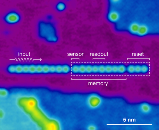
Remote detection and recording of atomic-scale spin dynamics
Atomic spin structures assembled by means of scanning tunneling microscopy (STM) provide valuable insight into the understanding of atomic-scale magnetism. Among the major challenges are the detection and subsequent read-out of ultrafast spin dynamics due to a dichotomy in travel speed of these dynamics and the probe tip. Here, we present a device composed of individual Fe atoms that allows for remote detection of spin dynamics. We have characterized the device and used it to detect the presence of spin waves originating from an excitation induced by the STM tip several nanometres away; this may be extended to much longer distances. The device contains a memory element that can be consulted seconds after detection, similar in functionality to e.g. a single photon detector. We performed statistical analysis of the responsiveness to remote spin excitations and corroborated the results using basic calculations of the free evolution of coupled quantum spins.
15 notes
·
View notes
Text
Postdoctoral Research Associate- Thin Film Synthesis and Characterization of Quantum Materials
Job title: Postdoctoral Research Associate- Thin Film Synthesis and Characterization of Quantum Materials Company: Oak Ridge National Laboratory Job description: , you will focus on the growth of thin film and heterostructure quantum materials utilizing molecular beam epitaxy, and probing the… thin film synthesis, ultrahigh vacuum techniques such as scanning tunneling microscopy and…
0 notes