#VHDL combinational logic
Explore tagged Tumblr posts
Visit Tumblr Blog
Explore Tumblr blogs with no restrictions, modern design and the best experience.
Last Seen Tumblr Blogs


Fun Fact
Total funding amounts to $125.3M.
Text
youtube
VHDL Tutorial - Complete Guide to VHDL Process Statement for Beginners [20 mins] [Easy Way]
Welcome to this comprehensive VHDL tutorial where we will dive into the VHDL process statement. In this easy-to-follow guide, we will take you through the syntax and usage of the VHDL process statement, catering especially to beginners. This tutorial will provide you with a thorough understanding of the VHDL process and how it can be effectively implemented in your projects.
Subscribe to "Learn And Grow Community"
YouTube : https://www.youtube.com/@LearnAndGrowCommunity
LinkedIn Group : https://www.linkedin.com/groups/7478922/
Blog : https://LearnAndGrowCommunity.blogspot.com/
Facebook : https://www.facebook.com/JoinLearnAndGrowCommunity/
Twitter Handle : https://twitter.com/LNG_Community
DailyMotion : https://www.dailymotion.com/LearnAndGrowCommunity
Instagram Handle : https://www.instagram.com/LearnAndGrowCommunity/
Follow #LearnAndGrowCommunity
#VHDL tutorial#VHDL process statement#VHDL syntax#VHDL beginner's guide#VHDL tutorial for beginners#VHDL process explained#VHDL process tutorial#VHDL sequential logic#VHDL combinational logic#VHDL development#VHDL design#VHDL FPGA#VHDL ASIC#VHDL circuits#VHDL learning#VHDL education#VHDL digital design#VHDL programming#HDL Design#Digital Design#Verilog#VHDL#FPGA#Simulation#Project#Synthesis#Training#Career#Programming Language#Xilinx
1 note
·
View note
Text
Understanding FPGA Architecture: Key Insights
Introduction to FPGA Architecture
Imagine having a circuit board that you could rewire and reconfigure as many times as you want. This adaptability is exactly what FPGAs offer. The world of electronics often seems complex and intimidating, but understanding FPGA architecture is simpler than you think. Let’s break it down step by step, making it easy for anyone to grasp the key concepts.
What Is an FPGA?
An FPGA, or Field Programmable Gate Array, is a type of integrated circuit that allows users to configure its hardware after manufacturing. Unlike traditional microcontrollers or processors that have fixed functionalities, FPGAs are highly flexible. You can think of them as a blank canvas for electrical circuits, ready to be customized according to your specific needs.
How FPGAs Are Different from CPUs and GPUs
You might wonder how FPGAs compare to CPUs or GPUs, which are more common in everyday devices like computers and gaming consoles. While CPUs are designed to handle general-purpose tasks and GPUs excel at parallel processing, FPGAs stand out because of their configurability. They don’t run pre-defined instructions like CPUs; instead, you configure the hardware directly to perform tasks efficiently.
Basic Building Blocks of an FPGA
To understand how an FPGA works, it’s important to know its basic components. FPGAs are made up of:
Programmable Logic Blocks (PLBs): These are the “brains” of the FPGA, where the logic functions are implemented.
Interconnects: These are the wires that connect the logic blocks.
Input/Output (I/O) blocks: These allow the FPGA to communicate with external devices.
These elements work together to create a flexible platform that can be customized for various applications.
Understanding Programmable Logic Blocks (PLBs)
The heart of an FPGA lies in its programmable logic blocks. These blocks contain the resources needed to implement logic functions, which are essentially the basic operations of any electronic circuit. In an FPGA, PLBs are programmed using hardware description languages (HDLs) like VHDL or Verilog, enabling users to specify how the FPGA should behave for their particular application.
What are Look-Up Tables (LUTs)?
Look-Up Tables (LUTs) are a critical component of the PLBs. Think of them as small memory units that can store predefined outputs for different input combinations. LUTs enable FPGAs to quickly execute logic operations by “looking up” the result of a computation rather than calculating it in real-time. This speeds up performance, making FPGAs efficient at performing complex tasks.
The Role of Flip-Flops in FPGA Architecture
Flip-flops are another essential building block within FPGAs. They are used for storing individual bits of data, which is crucial in sequential logic circuits. By storing and holding values, flip-flops help the FPGA maintain states and execute tasks in a particular order.
Routing and Interconnects: The Backbone of FPGAs
Routing and interconnects within an FPGA are akin to the nervous system in a human body, transmitting signals between different logic blocks. Without this network of connections, the logic blocks would be isolated and unable to communicate, making the FPGA useless. Routing ensures that signals flow correctly from one part of the FPGA to another, enabling the chip to perform coordinated functions.
Why are FPGAs So Versatile?
One of the standout features of FPGAs is their versatility. Whether you're building a 5G communication system, an advanced AI model, or a simple motor controller, an FPGA can be tailored to meet the exact requirements of your application. This versatility stems from the fact that FPGAs can be reprogrammed even after they are deployed, unlike traditional chips that are designed for one specific task.
FPGA Configuration: How Does It Work?
FPGAs are configured through a process called “programming” or “configuration.” This is typically done using a hardware description language like Verilog or VHDL, which allows engineers to specify the desired behavior of the FPGA. Once programmed, the FPGA configures its internal circuitry to match the logic defined in the code, essentially creating a custom-built processor for that particular application.
Real-World Applications of FPGAs
FPGAs are used in a wide range of industries, including:
Telecommunications: FPGAs play a crucial role in 5G networks, enabling fast data processing and efficient signal transmission.
Automotive: In modern vehicles, FPGAs are used for advanced driver assistance systems (ADAS), real-time image processing, and autonomous driving technologies.
Consumer Electronics: From smart TVs to gaming consoles, FPGAs are used to optimize performance in various devices.
Healthcare: Medical devices, such as MRI machines, use FPGAs for real-time image processing and data analysis.
FPGAs vs. ASICs: What’s the Difference?
FPGAs and ASICs (Application-Specific Integrated Circuits) are often compared because they both offer customizable hardware solutions. The key difference is that ASICs are custom-built for a specific task and cannot be reprogrammed after they are manufactured. FPGAs, on the other hand, offer the flexibility of being reconfigurable, making them a more versatile option for many applications.
Benefits of Using FPGAs
There are several benefits to using FPGAs, including:
Flexibility: FPGAs can be reprogrammed even after deployment, making them ideal for applications that may evolve over time.
Parallel Processing: FPGAs excel at performing multiple tasks simultaneously, making them faster for certain operations than CPUs or GPUs.
Customization: FPGAs allow for highly customized solutions, tailored to the specific needs of a project.
Challenges in FPGA Design
While FPGAs offer many advantages, they also come with some challenges:
Complexity: Designing an FPGA requires specialized knowledge of hardware description languages and digital logic.
Cost: FPGAs can be more expensive than traditional microprocessors, especially for small-scale applications.
Power Consumption: FPGAs can consume more power compared to ASICs, especially in high-performance applications.
Conclusion
Understanding FPGA architecture is crucial for anyone interested in modern electronics. These devices provide unmatched flexibility and performance in a variety of industries, from telecommunications to healthcare. Whether you're a tech enthusiast or someone looking to learn more about cutting-edge technology, FPGAs offer a fascinating glimpse into the future of computing.
2 notes
·
View notes
Text
Mastering VLSI Design: The Path to a Promising Career in Semiconductor Industry
The Rising Demand for VLSI Professionals
The semiconductor industry is experiencing a dramatic shift, powered by the growing demand for smaller, faster, and more efficient chips in everything from smartphones to electric vehicles. Very-Large-Scale Integration (VLSI) design plays a critical role in this transformation, enabling the integration of millions of transistors onto a single chip. As technology continues to evolve, the need for skilled VLSI engineers is expanding at an unprecedented rate. This demand has opened up a world of opportunities for those interested in chip design and semiconductor engineering. Companies worldwide are investing in VLSI talent to maintain a competitive edge, making this an ideal time for students and professionals to build a career in the field. Whether it’s designing system-on-chip (SoC) solutions or optimizing embedded systems, VLSI experts are becoming increasingly vital to the tech ecosystem.
Understanding the Fundamentals of VLSI Design
VLSI design involves the process of creating integrated circuits by combining thousands or even millions of transistors into a single chip. This complex engineering task requires a deep understanding of electronic circuit design, semiconductor physics, and design tools like Verilog, SystemVerilog, and VHDL. The curriculum in most vlsi training institutes includes modules on front-end and back-end design, logic synthesis, timing analysis, and verification methods. The end goal is to produce high-performance chips that are also power-efficient and cost-effective. VLSI engineers must possess strong analytical skills, a deep interest in electronics, and a passion for solving real-world problems. As technology nodes continue to shrink from 7nm to 3nm and beyond, the challenges in VLSI design grow more complex—demanding not just theoretical knowledge but also hands-on experience in state-of-the-art tools and practices.
Exploring Career Opportunities in VLSI
A career in VLSI is not only intellectually rewarding but also financially lucrative. From design engineers to physical design experts and verification engineers, the job roles in this domain are diverse and highly specialized. Each position plays a crucial part in bringing a semiconductor product from concept to fabrication. What makes VLSI especially appealing is the steady demand from both startups and tech giants involved in AI, IoT, and 5G innovation. Particularly in India, the ecosystem around semiconductor design is growing, creating an urgent need for competent professionals. The rise of online vlsi training institutes in bangalore has made it easier for aspiring engineers to access high-quality education and training without geographical constraints. With remote learning tools, recorded sessions, and access to simulators, these platforms are revolutionizing how VLSI education is delivered, allowing learners to gain industry-relevant skills from the comfort of their homes.
Key Skills and Tools Every VLSI Engineer Should Learn
To thrive in the VLSI domain, aspiring engineers must master a combination of technical skills and practical tools. On the technical side, knowledge of digital electronics, CMOS design principles, and signal integrity is foundational. On the software front, proficiency in EDA (Electronic Design Automation) tools like Cadence, Synopsys, and Mentor Graphics is a must. Additionally, scripting languages such as Perl, Python, and Tcl are used to automate repetitive design and verification tasks. Industry expectations are high, and candidates are often evaluated not just for their academic background but for their problem-solving ability, project experience, and understanding of real-time design constraints. VLSI is a continuously evolving field, and engineers must commit to lifelong learning to stay ahead. Regularly updating one’s knowledge through webinars, certifications, and self-guided projects is crucial to success in this fast-paced industry.
Choosing the Right Institute for VLSI Training
Given the complexity and depth of the VLSI field, selecting the right training institute becomes a vital step in one’s professional journey. The ideal institute offers a blend of theoretical instruction and practical exposure, mentored by industry veterans. It should provide access to real-world design tools, capstone projects, and placement support. Moreover, flexibility in learning schedules and a structured curriculum aligned with industry requirements can make a significant difference. One such platform that offers all these features is takshila-vlsi.com, a trusted name in the VLSI education space. With a commitment to quality and innovation, Takshila VLSI equips learners with the skills needed to succeed in the semiconductor industry, bridging the gap between academic knowledge and practical application.
0 notes
Text
Hardware Reconfigurable Devices
Hardware reconfigurable devices, such as Field-Programmable Gate Arrays (FPGAs) and Complex Programmable Logic Devices (CPLDs), enable dynamic customization of hardware functionality. Unlike traditional Application-Specific Integrated Circuits (ASICs), which have fixed designs, reconfigurable devices can be programmed to perform a wide range of tasks post-manufacturing. This flexibility is achieved through programmable logic blocks and interconnects.
FPGAs are particularly powerful, offering high parallelism and configurability for tasks such as digital signal processing, artificial intelligence, and cryptography. They excel in applications requiring low latency, real-time processing, or iterative prototyping. In contrast, CPLDs are simpler and used for control-oriented applications like glue logic or signal routing.
Reconfigurable hardware combines the performance of hardware solutions with the adaptability of software. Designs are typically implemented using hardware description languages (HDLs) like VHDL or Verilog and can be updated as requirements evolve.
These devices are widely used in industries such as telecommunications, automotive, and aerospace, where they provide a cost-effective solution to meet changing standards or improve system performance. Advances in tools and technologies continue to enhance their usability, enabling faster deployment of custom hardware solutions.
For More : https://tinyurl.com/u3r79skd

0 notes
Text
Learning ASIC Design Online to Advance a Rewarding Career
The need for qualified ASIC (Application-Specific Integrated Circuit) designers has skyrocketed in line with the fast technological changes. Designed to satisfy individuals driven to succeed in electronics and embedded systems, an ASIC design course provides a portal into the fascinating field of custom chip design. Unlike general-purpose integrated circuits, ASICs are specialist circuits tailored for a certain application. From consumer electronics to healthcare and automotive, these chips are very essential in devices of many kinds. Learning ASIC design gives engineers the technical tools they need to create customized solutions, hence providing interesting career routes in sectors in demand.
Essential Learning Materials for an ASIC Design Course
Usually covering both basic and advanced subjects, an ASIC design course combines theory with useful design methods. Starting with the foundations of digital design, students next explore hardware description languages (HDLs) such as Verilog and VHDL, which are important for specifying circuit behavior. To guarantee circuits satisfy high-performance criteria, the course moves through logic synthesis, functional verification, and timing analysis. Emphasizing practical laboratories, students get real-world experience working with instruments of industrial standard. This extensive course guarantees that students grasp the design process completely, therefore equipping them for the demanding requirements of ASIC development employment.
Online ASIC Design Training's advantages
Online ASIC design training has made it simpler than ever in recent years to gain these specialist abilities free from geographical restrictions. Online courses let students and professionals study at their speed by offering flexible scheduling. These classes are meant to fit working professionals, students, and even amateurs hoping to become ASIC designers. Online training offers a collaborative learning environment using interactive modules, live sessions, and forums. Expert advice and peer conversations help students create a dynamic environment that replicates real-world situations while keeping flexibility for their hectic lives.
Employment Prospectives and Professional Development Using ASIC Design Skills
Demand for ASIC designers is strong in many areas, but especially in tech-driven sectors such as IoT, 5G, and artificial intelligence. Businesses always want talented ASIC designers to provide effective, small-sized, high-performance processors. Completing an ASIC design course lets professionals work as physical design experts, verification engineers, and ASIC design engineers with employment paying attractive rates and opportunities for career development. Furthermore, given the growing complexity of digital goods, ASIC knowledge of new technologies is always in demand, so this ability is not only useful but also future-proof in a sector that is always changing.
Selecting the Correct Platform for ASIC Design Education
Achieving one's professional objectives depends on choosing the right platform to learn ASIC design. Prospective students should search for courses offering a theoretical background as well as real-world industry tool experience like Cadence, Synopsys, and Mentor Graphics. The learning process may be improved with thorough assistance via digital laboratories, lecture recordings, and Q&A sessions, among other online tools. Many online ASIC design training courses include certificates that enhance a candidate's profile and provide credibility, therefore helping them stand out to companies in a crowded employment market. Selecting a respectable course guarantees students' readiness for the expectations of the sector.
Conclusion
Following an ASIC design course—especially via online resources—opens a world of possibilities in integrated circuit design. Those with specific expertise and useful abilities may boldly join the market in fields dependent on high-performance, customized chips. For novices as well as seasoned experts, the adaptability of online ASIC design training lets students acquire industry-relevant knowledge from anywhere. Platforms like takshila-vlsi.com provide priceless training materials for people wanting to improve their VLSI abilities and flourish in ASIC design, therefore bridging the knowledge gap between expertise required in today's tech scene.
0 notes
Text
COMP4300 Lab Exercise Three solved
Objective This lab develops some remaining datapath building blocks for the Aubie processor . It will be combined with the Aubie control logic to make a working cpu in Lab 4. Instructions Develop VHDL for the following components. You should define an architecture for each of the entities given below. You should test each entity by developing simulation files for the entity. Your architecture…
0 notes
Text
Solved CENG2010 Lab 1: Introduction to VHDL
1. Given the following combinational logic circuit: a. Implement the circuit using VHDL. Use four switches (i.e. sw0 to sw3) as the inputs, and use one LED (i.e. led0) as the output. [20 marks] 2. Using VHDL, turn on the LEDs (i.e. led0 to led7) by the switches (i.e. sw0 to sw7) in the following manners: a. led0 will be ON when sw0 is ON b. led1 will be ON when sw1 is ON c. led2 will be ON when…
0 notes
Text
Understanding FPGA Architecture: Key Insights
Introduction to FPGA Architecture
Imagine having a circuit board that you could rewire and reconfigure as many times as you want. This adaptability is exactly what FPGAs offer. The world of electronics often seems complex and intimidating, but understanding FPGA architecture is simpler than you think. Let’s break it down step by step, making it easy for anyone to grasp the key concepts.
What Is an FPGA?
An FPGA, or Field Programmable Gate Array, is a type of integrated circuit that allows users to configure its hardware after manufacturing. Unlike traditional microcontrollers or processors that have fixed functionalities, FPGAs are highly flexible. You can think of them as a blank canvas for electrical circuits, ready to be customized according to your specific needs.
How FPGAs Are Different from CPUs and GPUs
You might wonder how FPGAs compare to CPUs or GPUs, which are more common in everyday devices like computers and gaming consoles. While CPUs are designed to handle general-purpose tasks and GPUs excel at parallel processing, FPGAs stand out because of their configurability. They don’t run pre-defined instructions like CPUs; instead, you configure the hardware directly to perform tasks efficiently.
Basic Building Blocks of an FPGA
To understand how an FPGA works, it’s important to know its basic components. FPGAs are made up of:
Programmable Logic Blocks (PLBs): These are the “brains” of the FPGA, where the logic functions are implemented.
Interconnects: These are the wires that connect the logic blocks.
Input/Output (I/O) blocks: These allow the FPGA to communicate with external devices.
These elements work together to create a flexible platform that can be customized for various applications.
Understanding Programmable Logic Blocks (PLBs)
The heart of an FPGA lies in its programmable logic blocks. These blocks contain the resources needed to implement logic functions, which are essentially the basic operations of any electronic circuit. In an FPGA, PLBs are programmed using hardware description languages (HDLs) like VHDL or Verilog, enabling users to specify how the FPGA should behave for their particular application.
What are Look-Up Tables (LUTs)?
Look-Up Tables (LUTs) are a critical component of the PLBs. Think of them as small memory units that can store predefined outputs for different input combinations. LUTs enable FPGAs to quickly execute logic operations by “looking up” the result of a computation rather than calculating it in real-time. This speeds up performance, making FPGAs efficient at performing complex tasks.
The Role of Flip-Flops in FPGA Architecture
Flip-flops are another essential building block within FPGAs. They are used for storing individual bits of data, which is crucial in sequential logic circuits. By storing and holding values, flip-flops help the FPGA maintain states and execute tasks in a particular order.
Routing and Interconnects: The Backbone of FPGAs
Routing and interconnects within an FPGA are akin to the nervous system in a human body, transmitting signals between different logic blocks. Without this network of connections, the logic blocks would be isolated and unable to communicate, making the FPGA useless. Routing ensures that signals flow correctly from one part of the FPGA to another, enabling the chip to perform coordinated functions.
Why are FPGAs So Versatile?
One of the standout features of FPGAs is their versatility. Whether you're building a 5G communication system, an advanced AI model, or a simple motor controller, an FPGA can be tailored to meet the exact requirements of your application. This versatility stems from the fact that FPGAs can be reprogrammed even after they are deployed, unlike traditional chips that are designed for one specific task.
FPGA Configuration: How Does It Work?
FPGAs are configured through a process called “programming” or “configuration.” This is typically done using a hardware description language like Verilog or VHDL, which allows engineers to specify the desired behavior of the FPGA. Once programmed, the FPGA configures its internal circuitry to match the logic defined in the code, essentially creating a custom-built processor for that particular application.
Real-World Applications of FPGAs
FPGAs are used in a wide range of industries, including:
Telecommunications: FPGAs play a crucial role in 5G networks, enabling fast data processing and efficient signal transmission.
Automotive: In modern vehicles, FPGAs are used for advanced driver assistance systems (ADAS), real-time image processing, and autonomous driving technologies.
Consumer Electronics: From smart TVs to gaming consoles, FPGAs are used to optimize performance in various devices.
Healthcare: Medical devices, such as MRI machines, use FPGAs for real-time image processing and data analysis.
FPGAs vs. ASICs: What’s the Difference?
FPGAs and ASICs (Application-Specific Integrated Circuits) are often compared because they both offer customizable hardware solutions. The key difference is that ASICs are custom-built for a specific task and cannot be reprogrammed after they are manufactured. FPGAs, on the other hand, offer the flexibility of being reconfigurable, making them a more versatile option for many applications.
Benefits of Using FPGAs
There are several benefits to using FPGAs, including:
Flexibility: FPGAs can be reprogrammed even after deployment, making them ideal for applications that may evolve over time.
Parallel Processing: FPGAs excel at performing multiple tasks simultaneously, making them faster for certain operations than CPUs or GPUs.
Customization: FPGAs allow for highly customized solutions, tailored to the specific needs of a project.
Challenges in FPGA Design
While FPGAs offer many advantages, they also come with some challenges:
Complexity: Designing an FPGA requires specialized knowledge of hardware description languages and digital logic.
Cost: FPGAs can be more expensive than traditional microprocessors, especially for small-scale applications.
Power Consumption: FPGAs can consume more power compared to ASICs, especially in high-performance applications.
Conclusion
Understanding FPGA architecture is crucial for anyone interested in modern electronics. These devices provide unmatched flexibility and performance in a variety of industries, from telecommunications to healthcare. Whether you're a tech enthusiast or someone looking to learn more about cutting-edge technology, FPGAs offer a fascinating glimpse into the future of computing.
0 notes
Text
Intel’s Silicon Mobility OLEA U310 SoC Boosts EV Progress
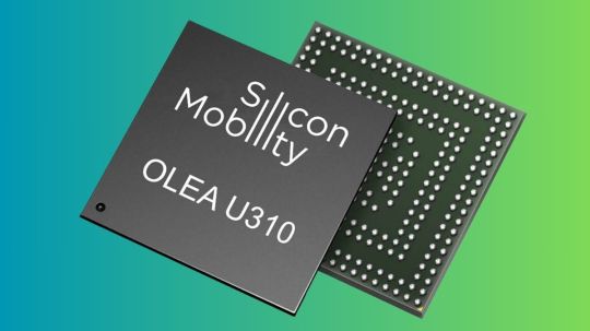
Silicon Mobility OLEA U310
One of the main obstacles to purchasing an electric vehicle (EV) is still its expensive cost, which deters many prospective consumers worldwide. Due in large part to the high expense of developing improved battery and e-motor technologies, electric vehicles (EVs) are now more expensive to construct than conventional gasoline-powered vehicles. Improving the efficiency of current battery technology at the vehicle level through energy savings and better interaction with EV station infrastructure is the short-term solution.
With the release of the new OLEA U310 system-on-chip (SoC) today, Silicon Mobility, an Intel company, has successfully addressed this precise difficulty. The entire performance of electric cars (EVs) will be greatly enhanced by this next-generation technology, which will also expedite the design and production processes and expand SoC services to guarantee smooth operation across a variety of EV station platforms.
Mobility in Silicon
The new SoC, which is a first for the industry, is the first all-in-one solution that combines software and hardware, and it is designed to meet the requirements of distributed software-based electrical architectures for powertrain domain control. With its distinct hybrid and heterogeneous architecture, the OLEA 310 FPCU can take the place of up to six conventional microcontrollers in a system configuration that includes an on-board charger, a gearbox, an inverter, a motor, and a DC-DC converter. Original equipment manufacturers (OEMs) and Tier 1 suppliers can regulate a variety of power and energy functions simultaneously and in real time with the 310 FPCU.
Create a function grouping for your e-powertrain
The OLEA U310 is a recent addition to the Silicon Mobility FPCU line. Its design matches distributed software requirements for powertrain domain control in electrical/electronic designs. Beyond the capabilities of conventional microcontrollers, the OLEA U310 is constructed with a novel hybrid and heterogeneous architecture that embeds numerous software and hardware programmable processing and control units seamlessly integrating functional safety and the cybersecurity into its fundamental design. It hosts and connects, on a single chip, the essential event-based multifunction control requirements with the time-based and multitask software application needs.
Created with the newest demands in automobile control in mind
The OLEA U310 can do more than only powertrain tasks. Additional uses for this adaptable system-on-a-chip include:
Systems for Chassis Control
Fusion of Data
Compressor air
System for Thermal Management
Different Control Mechanisms
EV makers may create a more integrated and effective control system that improves control and performance by utilising the adaptability of the OLEA U310.
Authority of the AxEC
For direct sensor and actuator interfacing, the Advanced eXecution & Event Control (AxEC) unit integrates programmable hardware, mathematical coprocessors, and adjustable peripherals. The core of the FPCU architecture is the programmable hardware known as the Flexible Logic Units (FLU). It is a programmable logic fabric that can be designed using common hardware description languages like Verilog or VHDL. It is furnished with flip-flops, SRAM, lookup tables, and signal processing units. 1-4 FLU partitions are a notion that is introduced by the OLEA U Series.
CPUs are in charge of high-level and low-response-time software, while AxEC deals with real-time control and fast-response processing. For particular jobs, designers have the option of using CPU or AxEC; nevertheless, AxEC usually performs sophisticated processing, minimising CPU utilisation. Regardless of the number or frequency of events, hardware processing guarantees prompt, accurate responses.
Protected by OLEA SiLant
The greatest level of automotive safety integrity specified by the ISO 26262 functional safety standard, ASIL-D design ready, is met by the FPCU. The OLEA U Series Safety Integrity Agent (SiLant) is in charge of identifying, containing, and responding to errors in nanoseconds. It is the key hub for all safety measures integrated within the FPCU. SiLant detects software and system faults in addition to latent and transient faults at the semiconductor level.
OLEA U FLU provides safe multitasking and function grouping with unified firmware virtualization from CPU down to FLU level with the advent of multi-CPU and multi-FLU. OLEA U offers assurances and a deterministic architecture. Worst-Scene Performance It’s time to create applications that require safety.
Protected by OLEA FHSM
For the best defence against current and potential threats, the latest generation of FPCU is available. A subsystem integrated into the OLEA U Series that complies with the ISO 21434 automotive cybersecurity standard and EVITA Full is called the Flexible Hardware Security Module (FHSM). Its specialised programmable hardware allows it to contain hardware-accelerated security functions that can be used to improve protection or keep an eye out for any system security breaches. This special feature makes use of a wider range of cryptographic techniques to enable safe real-time communications as well as secure software updates and execution.
Mobility of Silicon
Together with the bill of material (BoM) reduction, preliminary data indicates that compared to current EVs, there will be a 5% increase in energy efficiency, a 25% reduction in motor size for the same power, a 35% decrease in cooling requirements, and a 30% reduction in passive component size. With fewer components to incorporate, the new Silicon Mobility technology enables EV makers to develop software-defined electric vehicles with superior performance, increased range, and potentially cheaper production costs. The industry’s transition to an all-electric and software-defined future will be accelerated by the new solution, which also enhances Intel Automotive’s current line of AI-enhanced software-defined vehicle (SDV) SoCs.
Silicon Mobility OLEA U310 Features
2nd generation of FPCU
3x Cortex-R52 @ 350MHz – 2196 DMIPS
AxEC 2.0: 2x FLUs @ 175Mhz – 400 GOPS + 9.1 GMAC
SILant 2.0: Safe and Determinist Multi-Core/FLU
Flexible HSM: HW & SW EVITA Full
8MB of P-Flash, 256kB of D-Flash, 1MB of SRAM
CAN FD, CAN XL, Ethernet
ISO/SAE 21434 certifieISO 26262 ASIL-D & ISO/SAE 21434 compliant
AEC-Q100 Grade 1
292 BGA
Read more on Govindhtech.com
0 notes
Text
VHDL Assignment #2: Combinational Circuit Using VHDL Concurrent Statements
Instructions Due date: Friday, October 9, 2020 by 5pm. Submission is in teams using myCourses (only one team member submits). In the report, provide the names and McGill IDs of the team members. Late submissions will incur penalties as described in the course syllabus. 2 Introduction In this assignment you will be required to write simple logic functions in VHDL employing the techniques you…

View On WordPress
0 notes
Text
That is a very neat idea!
If you like things like that you might want to look into VHDL ( I learned that... some years ago, but have not touched it since ) or Verilog.
They are... programming languages for making logic gate logic.
You combine that with an FPGA, which is essentially a whole lot of NAND gates ( Which as I said, can represent any logic gate system ), and then you can make hardware... via software.
And yes, these essentially do things like your idea. Things that would take a CPU aaaaages to do, can be done very very fast. So you "just" have normal C code, but if it runs onto one of the problems it have hardware for, it uses the hardware.
This is also how graphics cards work, or just floating point operations!
It is insanely cool! :D
What is half-adder and full-adder combinational circuits?
So this question came up in the codeblr discord server, and I thought I would share my answer here too :3
First, a combinational circuit simply means a circuit where the outputs only depends on its input. ( combinational means "Combine" as in, combining the inputs to give some output )
It is a bit like a pure function. It is opposed to circuits like latches which remembers 1 bit. Their output depends on their inputs AND their state.
These circuits can be shown via their logic gates, or truth tables. I will explain using only words and the circuits, but you can look up the truth tablet for each of the circuits I talk about to help understand.

Ok, so an in the case of electronics is a circuit made with logic gates ( I... assume you know what they are... Otherwise ask and I can explain them too ) that adds 2 binary numbers, each which have only 1 character.
So one number is 1 or 0
And the other number is 1 or 0
So the possible outputs are are 0, 1 and 2.
Since you can only express from 0 to 1 with one binary number, and 0 to 3 with 2, we need to output 2 binary numbers to give the answer. So the output is 2 binary numbers
00 = 0
01 = 1
10 = 2
11 = 3 // This can never happen with a half adder. The max possible result is 2
Each character will be represented with a wire, and a wire is a 0 if it is low voltage (usually ground, or 0 volts) and a 1 if it is high voltage (Voltage depends. Can be 5 volts, 3.3, 12 or something else. )
BUT if you only use half adders, you can ONLY add 2 single character binary numbers together. Never more.
If you want to add more together, you need a full adder. This takes 3 single character binary numbers, and adds them and outputs a single 2 character number.
This means it have 3 inputs and 2 outputs.

We have 2 outputs because we need to give a result that is 0, 1, 2 or 3
Same binary as before, except now we CAN get a 11 (which is 3)
And we can chain full adders together to count as many inputs as we want.
So why ever use a half adder? Well, every logic gate cirquit can be made of NAND (Not and) gates, so we usually compare complexity in how many NAND gates it would take to make a circuit. More NAND gates needed means the circuit is slower and more expensive to make.
A half adder takes 5 NAND gates to make
A full adder takes 9 NAND gates.
So only use a full adder if you need one.
Geeks for Geeks have a page for each of the most normal basic cirquits:
I hope that made sense, and was useful :3
41 notes
·
View notes
Text
How To Choose Frontend Vs. Backend? A guide for Freshers

#VLSI frontend and backend are nothing but two different domains in the field of VLSI. The classification is based on the different steps involved in a typical ASIC design flow. Following diagram shows a typical design flow for an ASIC or SOC.
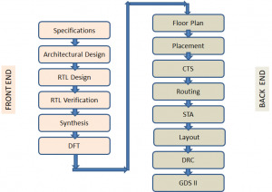
As it shows the design flow starts with a specification document which lists out the technical requirements needed in the chip design. It is followed by translating the specification to Architectural design. The architectural design involves designing the functional blocks and the communication protocol between them and translating them into actual modules that contain FSMs, combinational and sequential circuits etc. The architectural design is then modelled using a Hardware description language like Verilog/VHDL/System Verilog, which is the RTL design stage. The Functional Verification stage starts with a verification plan and a corresponding verification environment which describes and implements the method of proving the design correctness, using different Verification techniques. The design is refined until the HDL model is proved to be meeting the specifications.This stage is followed by Synthesis – a process of transforming the HDL design into a technology specific gate-level netlist, given all the specified constraints and optimization settings. DFT is a structural technique which facilitates a design to become testable after production. All the works till this stage are normally called as the Frontend of VLSI design and are executed by Frontend Engineers.
The next step in the ASIC Design flow is Placement and Routing which involves arranging approximate locations of a set of modules that need to be placed on a layout. Clock tree synthesis is a process which makes sure that the clock gets distributed evenly to all sequential elements in a design to fix the timing violations. This is followed by routing in which exact paths for the interconnection of standard cells and macros and I/O pins are determined.The file produced at the output of the layout is the GDSII (GDS2) file which is the file used by the foundry to fabricate the silicon. Gate level simulations and Static Timing Analysis (a method of validating the timing performance of a design by checking all possible paths for timing violations without having to simulate) are also done to make sure that the gate level design meets the timing requirements for correct design operations. All steps after logic synthesis are performed by Backend engineers and forms the Backend jobs.
Work of a Frontend Engineer
RTL Design/Coding
Synthesis
Functional Verification
DFT
Work of a Backend Engineer
Floor Planning
Placement
Clock Tree Synthesis
STA
Physical Verification
Which one has more career Opportunities?
With the advances being made in technologies like process geometries, feature size and product innovations on a daily basis, there is a constant need to design, develop and re-engineer integrated circuits (ICs). Since electronic products like mobile phones are being released with new features in shorter cycles, there is a healthy demand for qualified VLSI engineers to work on these products. Therefore, there is good scope for a career in the VLSI industry. The important point is that both the domains, front end and back end have their own advantages and have great career prospects. It is completely up to you which one to choose depending on your interest and confidence level, as both offer a great deal of learning and growth.
How to choose?
In order to become a front end engineer, one needs to have good knowledge of HDLs(Verilog/VHDL/SystemVerilog). It will be an added advantage if you have industry related protocol knowledge. So if you have ample digital fundamental knowledge, are fond of HDL coding, love debugging and want to have a sound understanding about the functionality of IC or chip you should definitely go for Front End. With the recent emergence of Artificial intelligence and its application towards VLSI opens up a huge scope for Front end engineers. In order to become a back end engineer, one needs to be well equipped with the concepts of digital electronics, CMOS and Analog Circuits, Scripting knowledge for automation, Hands on Tools for physical design, layout etc. If the above mentioned skills fascinates you then you can opt for Backend and there might be a chance to work in Foundry as well.
Challenges faced by a fresher to get into VLSI industry
Even though VLSI industry is a niche and has lots of career opportunities, on the flip side, industry is currently somewhat less reachable for fresh graduates, compared to other areas due to some particular reasons. Firstly, VLSI or chip design requires a deeper level of knowledge and skills than other electronics related fields .But our Universities are not catering 100% to the VLSI industry requirements. Secondly, VLSI chip design is expensive and requires access to high-cost, specialised electronic design automation (EDA) tools.
How can Chipedge help?
Chipedge offers various courses for fresh graduates both in frontend and backend domains, to choose from. The courses are well structured starting from building a strong foundation by emphasising on fundamental subjects like Digital, CMOS etc. Once the candidate becomes confident with the fundamental knowledge, we impart all the domain specific skills required for the VLSI industry, by giving hands on training on industry standard EDA tools (Synopsys).
1 note
·
View note
Text
VHDL Assignment #2: Combinational Circuit Using VHDL Concurrent Statements
Instructions Due date: Friday, October 9, 2020 by 5pm. Submission is in teams using myCourses (only one team member submits). In the report, provide the names and McGill IDs of the team members. Late submissions will incur penalties as described in the course syllabus. 2 Introduction In this assignment you will be required to write simple logic functions in VHDL employing the…

View On WordPress
0 notes
Text
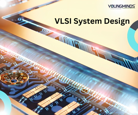
YoungMinds - VLSI System Design and It’s Importance
Full-form of VLSI is Very Large-Scale Integration, is the process of creating an integrated circuits (IC’s) by combining millions or billions of MOS transistors onto a single chip.
VLSI began in the 1970s when MOS integrated circuit (Metal Oxide Semiconductor) chips were developed and then widely adopted, enabling complex semiconductor and telecommunication technologies. The microprocessor and memory chips are VLSI devices.
VLSI is one of the most widely used technologies for microchip processors, integrated circuits (IC) and component designing. It was initially designed to support hundreds of thousands of transistor gates on a microchip which, as of 2012, exceeded several billion.
In VLSI, the programming languages for IC design are called hardware description languages (HDLs). These include VHDL, Verilog, System Verilog, C, and scripting languages like Perl and TCL. In VLSI, the development methodology a team follows is as important as the HDL used to build a new product.
Few Important Points of VLSI System Design: -
VLSI is a measure of the complexity of an integrated circuit
It deals with the Software
It deals with reading and converting signals from digital to analog and vice versa for a task
Need knowledge of computer programming languages like C, C++
Deals with Internet of things Machine Learning, UI design, Networking
Moreover, as the new-age technologies like machine learning, artificial intelligence, edge computing, cloud, etc. becomes mainstream, it needs to be backed up with highly efficient and specialized chip design. Typically, electronic circuits incorporate a CPU, RAM, ROM, and other peripherals on a single PCBA.
If anyone searching VLSI System Design Services to make your ideas into reality – my best suggestion is “Youngminds” - Realizing product and software development for a wide range of application areas on cutting-edge technologies like electronic chip design flow from specification to GDSII on latest node technologies, with special focus on RTL/FPGA Design, design verification and FPGA emulation.
“Young Minds” VLSI System Design Services: -
Micro-Architecture development for given specifications
SoC Design / ARM-based SoC architecture designs
RTL Integration & IP subsystem development
Full-Chip / SoC Level Design with Verilog, VHDL, System Verilog
Migration from FPGA to ASIC
Lint, CDC Checks and writing waivers
Integration of digital and analog blocks (Like SERDES PMA + PCS or DDR + Phy etc.,)
Synthesis, STA Constraints for both ASIC and FPGA
Logic equivalency and formality checks
Hands-on experience on Various Industrial EDA tools
Optimization of Power, Area and timing tradeoff
FPGA Prototyping on Xilinx / Altera FPGA Boards
High-Speed protocol Interfaces: -
PCIe Gen1,2,3,4,5 With PIPE / SERDES
Ethernet 100G, 40G, 10G, 1G
USB 3.0, USB 2.0 host and device controllers
AXI, AHB
Other Interfaces like APB / SPI / UART / I2C
Not only VLSI System Design and Development Services, the best thing is “Youngminds” is also provides Training Programs to help students / Engineers and customers get to productivity faster.
Still need more information about “Young Minds” – Visit https://ymtsindia.com/
VLSI System Design Services: - https://ymtsindia.com/VLSI-system-design
Tomorrow will be too late, it’s now or never - Call / WhatsApp us for any Queries @ +91-8688400282
vlsi system design, vlsi design services, vlsi system design services, youngminds vlsi system design
0 notes
Text
Getting Started with VHDL Coding
Introduction In this lab you will learn the basics of the Altera Quartus II FPGA design software through following a step-by-step tu-torial, and use it to implement combinational logic circuits described in VHDL. You will also learn the basics of digital simulation using the ModelSim simulation program. Learning Outcomes After completing this lab you should know how to: Run the Intel Quartus…

View On WordPress
0 notes
Text
Parallel Input Serial Output Shift Register Verilog Code

8-bit parallel-in/serial-out shift register
The testbech for the Serial shift register Serial Input Serial Output Shift Register Exercizes 1. In test bench the shift register is instantiated with N=2. Verify that it behaves as expected. Repead the testbench and verification for N=4 2. Write the above code for left shift in place of right shift. The data now comes out of the MSB. Design of 4 Bit Parallel IN.Output. Need vhdl code for 16 bit serial-in, serial-out shift register. 4-bit parallel shift register code. Bit serial arithmetic Vs Digit serial Arithmetic. 4 Bit Sipo Shift Register Vhdl Code Vhdl code for 4 bit shift register allaboutfpgacom, vhdl code for shift register can be categorised in serial in serial out shift. The following code models a four-bit parallel in shift left register with load and shift enable signal. Module Parallelinserialoutloadenablebehavior(input Clk, input ShiftIn, input 3:0 ParallelIn, input load, input ShiftEn, output ShiftOut, output. The following code models a four-bit parallel in shift left register with load and shift enable signal. Module Parallelinserialoutloadenablebehavior(input Clk, input ShiftIn, input 3:0 ParallelIn, input load, input ShiftEn, output ShiftOut, output. In Parallel In Serial Out (PISO) shift registers, the data is loaded onto the register in parallel format while it is retrieved from it serially.Figure 1 shows a PISO shift register which has a control-line. And combinational circuit (AND and OR gates) in addition to the basic register components fed with clock and clear pins.

The 74LV165 is an 8-bit parallel-load or serial-in shift register with complementary serial outputs (Q7 and Q7) available from the last stage. When the parallel-load input (PL) is LOW, parallel data from the inputs D0 to D7 are loaded into the register asynchronously. When input PL is HIGH, data enters the register serially at the input DS. It shifts one place to the right (Q0→Q1→Q2, etc.) with each positive-going clock transition. This feature allows parallel-to-serial converter expansion by tying the output Q7 to the input DS of the succeeding stage.
The clock input is a gate-OR structure which allows one input to be used as an active LOW clock enable input (CE) input. The pin assignment for the inputs CP and CE is arbitrary and can be reversed for layout convenience. The LOW-to-HIGH transition of the input CE should only take place while CP HIGH for predictable operation. Either the CP or the CE should be HIGH before the LOW-to-HIGH transition of PL to prevent shifting the data when PL is activated.
Features and benefits
Wide supply voltage range from 1.0 V to 5.5 V
Synchronous parallel-to-serial applications
Optimized for low voltage applications: 1.0 V to 3.6 V
Synchronous serial input for easy expansion
Latch-up performance exceeds 250 mA
5.5 V tolerant inputs/outputs
Direct interface with TTL levels (2.7 V to 3.6 V)
Power-down mode
Complies with JEDEC standards:
JESD8-5 (2.3 V to 2.7 V)
JESD8B/JESD36 (2.7 V to 3.6 V)
JESD8-1A (4.5 V to 5.5 V)
ESD protection:
HBM JESD22-A114-A exceeds 2000 V
MM JESD22-A115-A exceeds 200 V
Specified from -40°C to +85°C and from -40°C to +125°C
Parametrics
Type numberVCC (V)Logic switching levelsOutput drive capability (mA)tpd (ns)fmax (MHz)No of bitsTamb (°C)Rth(j-c) (K/W)74LV165DProduction1.0 - 5.5TTL± 1218788low-40~125919.351SO1674LV165DB NRNDNot for design inSSOP1674LV165PWProduction1.0 - 5.5TTL± 1218788low-40~1251203.348.7TSSOP16
Package
PackagePackage informationReflow-/Wave solderingStatus74LV165D SO16 (SOT109-1)SOT109-1SO-SOJ-REFLOW SO-SOJ-WAVE Reel 13' Q1/T1Active74LV165D74LV165D,118 (9351 560 60118)Bulk PackActive74LV165D74LV165D,112 (9351 560 60112)74LV165DB NRND SSOP16 (SOT338-1)SOT338-1SSOP-TSSOP-VSO-REFLOW SSOP-TSSOP-VSO-WAVE Reel 13' Q1/T1ActiveLV16574LV165DB,118 (9351 660 30118)Bulk PackActiveLV16574LV165DB,112 (9351 660 30112)74LV165PW TSSOP16 (SOT403-1)SOT403-1SSOP-TSSOP-VSO-WAVE Reel 13' Q1/T1ActiveLV16574LV165PW,118 (9351 745 40118)Bulk PackActiveLV16574LV165PW,112 (9351 745 40112)
Quality, reliability & chemical content
Leadfree conversion date74LV165D74LV165D,11874LV165Dweek 6, 2004144.910.239.78E71174LV165D74LV165D,11274LV165Dweek 6, 2004144.910.239.78E71174LV165DB NRND74LV165DB,11874LV165DBweek 12, 20051174LV165DB NRND74LV165DB,11274LV165DBweek 12, 20051174LV165PW74LV165PW,11874LV165PWweek 17, 2005144.910.239.78E71174LV165PW74LV165PW,11274LV165PWweek 17, 2005144.910.239.78E711
Quality and reliability disclaimer
Documentation (10)
File nameTitleTypeDate74LV1658-bit parallel-in/serial-out shift registerData sheet2017-03-17Nexperia_Selection_guide_2020Nexperia Selection Guide 2020Selection guide2020-01-31SO-SOJ-REFLOWFootprint for reflow solderingReflow soldering2009-10-08SO-SOJ-WAVEFootprint for wave solderingWave soldering2009-10-08SOT109-1plastic, small outline package; 16 leads; 1.27 mm pitch; 9.9 mm x 3.9 mm x 1.35 mm bodyPackage information2020-04-21SSOP-TSSOP-VSO-WAVEFootprint for wave solderingWave soldering2009-10-08SOT403-1plastic, thin shrink small outline package; 16 leads; 5 mm x 4.4 mm x 1.1 mm bodyPackage information2020-04-21SSOP-TSSOP-VSO-REFLOWFootprint for reflow solderingReflow soldering2009-10-08SSOP-TSSOP-VSO-WAVEFootprint for wave solderingWave soldering2009-10-08SOT338-1plastic, shrink small outline package; 16 leads; 0.65 mm pitch; 6.2 mm x 5.3 mm x 2 mm bodyPackage information2020-04-21
Support
If you are in need of design/technical support, let us know and fill in the answer form, we'll get back to you shortly.
Ordering, pricing & availability
Sample
As a Nexperia customer you can order samples via our sales organization or directly via our Online Sample Store: https://extranet.nexperia.com.
Sample orders normally take 2-4 days for delivery.
If you do not have a direct account with Nexperia our network of global and regional distributors is available and equipped to support you with Nexperia samples.
greatworks.netlify.com › Parallel Input Serial Output Shift Register Verilog Code ▄
Shift Register using verilog
I wrote a parallel in serial out shift register, which I present here. Module shiftreg32b (clk, reset, shift, carrega, in, regout); input clk; input reset, shift; input to an output in a combinational module in Verilog Verilog Illegal Reference to net 'OUT' What does this Verilog module do? It contains many explicit features which include parallel inputs, parallel outputs, synchronous reset, bidirectional serial input and bidirectional serial output. The below presented verilog code for 4-bit universal shift register acts as a uni-directional shift register for serial-in and serial-out mode,. Verilog Code for Parallel in Parallel Out Shift Register - Free download as Word Doc (.doc /.docx), PDF File (.pdf), Text File (.txt) or read online for free.
We will now consider a shift register. Our shift register has an s_in input entering on its left hand side. At each clock cycle, the content of the register shifts to the right and s_in enters into the leftmost bit or the MSB bit. The whole design also has and output that we are c calling s_out. At each clock cyccle the right most bit of the register comes out. The picture shows the scheme of the shift register. Here is the verilog implemmentation of shift register.
Explanation
Initially the reg value of undefined and hence we have placed 4'bxxxx in its value. Because of the assign statement the initial value of s_reg[0] is also 0. When the reset pulse is applied the r_reg becomes 0000 at the next rising edge of clock. Note that the period of the negative level of the reset sould last at least to the next rising edge of the clock At this stage, the value of s_out also becomes 0 ( right after the rising edge of the clock). Now the s_in value is supplied sometimes before the next rising edge of the clock. Now because of the assign statement the wire r_next is driven by the value of s_in and [3:1] bits of r_reg. And so, after the application of the s_in, at the next rising edge of the clock, the statement in the always loop takes effect. which essentially results in updating the r_reg value with its value shifted to right and s_in coming in at its MSB. The testbech for the Serial shift register
Serial Input Serial Output Shift Register
Exercizes 1. In test bench the shift register is instantiated with N=2. Verify that it behaves as expected. Repead the testbench and verification for N=4
Shift Register In Verilog
2. Write the above code for left shift in place of right shift. The data now comes out of the MSB. The data enters from LSB.
Parallel Load Shift Left Register verilog code
4 Bit Shift Register Verilog
This page covers Parallel Load Shift Left Register verilog code and test bench code of Parallel Load Shift Left Register.
Parallel Load Shift Left Register verilog code
Following is the verilog code of Parallel Load Shift Left Register.
module plsl(pl, sl, slin, Din, clk, reset, Q); input pl, sl, slin, clk, reset; input [7:0] Din; output [7:0] Q; reg [7:0] Q; always @ (posedge clk) begin if (~reset) begin if (sl) begin Q <= 'TICK {Q[6:0],slin}; end else if (pl) begin Q <= 'TICK Din; end end end always @ (posedge reset) begin Q <= 8'b00000000; end endmodule
Test code for Parallel Load Shift Left Register
Following is the test bench code of Parallel Load Shift Left Register.
I checked with Auto Installer. Edited 22 Feb 2017 by lamboom. And get this: After loading data, this window pops up stating that Sysmac is Up-to-Date. Then what's going on with 'Windows Configuring Sysmac Studio???? Sysmac studio v1.19.
module main; reg clk, reset, slin, sl, pl; reg [7:0] Din; wire [7:0] q; plsl plsl1(pl, sl, slin, Din, clk, reset, Q); initial begin forever begin clk <= 0; #5 clk <= 1; #5 clk <= 0; end end initial begin reset = 1; #12 reset = 0; #90 reset = 1; #12 reset = 0; end initial begin sl = 1; pl = 0; Din = 8'h42; #50 sl = 0; #12 pl = 1; #5 Din = 8'h21; #20 pl = 0; sl = 1; end initial begin forever begin slin = 0; #7 slin = 1; #8 slin = 0; end end endmodule
Verilog source codes
Low Pass FIR Filter Asynchronous FIFO design with verilog code D FF without reset D FF synchronous reset 1 bit 4 bit comparator All Logic Gates
RF and Wireless tutorials
WLAN802.11ac802.11adwimaxZigbeez-waveGSMLTEUMTSBluetoothUWBIoTsatelliteAntennaRADAR Drivers ed 4.02 assignment answers.
Share this page
Translate this page
ARTICLEST & M sectionTERMINOLOGIESTutorialsJobs & CareersVENDORSIoTOnline calculatorssource codesAPP. NOTEST & M World Website
0 notes