#Verilog
Explore tagged Tumblr posts
Visit Tumblr Blog
Explore Tumblr blogs with no restrictions, modern design and the best experience.
Last Seen Tumblr Blogs


Fun Fact
Tumblr has 16.74 million mobile monthly users in the US.
Note
I am not an EE but I have a live-in one installed in my house and rn I’m having to check that he’s not secretly verilog-official
also, metal + machines + tape measures (+ if you’re me also spaaaaace)
what's your favorite part of mechanical engineering & why are you not an electrical engineer (clearly superior /j)
Despite my immense enjoyment of ham radio and math, I really really really really love working with metal and machines. In all honesty if I weren't already not going to graduate on time I'd be double majoring :3
46 notes
·
View notes
Note
Assembly is not enough, i need to fuck my processor
VHDL or Verilog. I don't have any experience in Verilog, but have made some simple stuff on FPGAs with VHDL; it's pretty cool, but also quite frustrating since it's simultaneously the lowest level programming you'll probably ever do (as it is changing real hardware), but it's also quite abstract, so you don't really know what the compiler does; this makes fixing (heisen) bugs real tricky.
If you ment 'fuck my processor' more literally I recommend something with a LGA socket, because you will bend the pins of a PGA CPU. Also dry it off before reinserting it in your motherboard. I don't know how you'll get any real pleasure from it, but feel free to try!
5 notes
·
View notes
Text
i think i just found the single worst, most unreadable, least maintainable piece of code i have ever written
its an entire module built out of assign statements to output ports and ?: multiplexers

official middle finger to past me for making present me try to understand this
2 notes
·
View notes
Text
youtube
How to Download ModelSim Simulator for FREE! | Step by Step Guide in HINDI - [4 Min]
Welcome to our comprehensive tutorial on how to download ModelSim Simulator, the leading industry-standard digital simulation tool. In this step-by-step guide, we will walk you through the entire process, ensuring a hassle-free installation experience. ModelSim offers advanced simulation capabilities for digital designs, making it indispensable for hardware engineers, students, and enthusiasts alike.
In this video, we provide you with detailed instructions to download ModelSim Simulator effortlessly. Starting from checking the system requirements to ensuring optimal performance, we cover every essential aspect. We also discuss the licensing process and provide solutions to common installation errors that you may encounter. Our aim is to equip you with the knowledge and confidence to successfully install and utilize ModelSim Simulator in your projects.
Don't miss out on harnessing the power of ModelSim Simulator for your digital simulation needs. Watch this tutorial now and kickstart your journey towards efficient hardware design and verification!
🔔 Subscribe to our channel for more informative tutorials and updates! 🔔
Subscribe to "Learn And Grow Community"
YouTube : https://www.youtube.com/@LearnAndGrowCommunity
LinkedIn Group : linkedin.com/company/LearnAndGrowCommunity
Blog : https://LearnAndGrowCommunity.blogspot.com/
Facebook : https://www.facebook.com/JoinLearnAndGrowCommunity/
Twitter Handle : https://twitter.com/LNG_Community
DailyMotion : https://www.dailymotion.com/LearnAndGrowCommunity
Instagram Handle : https://www.instagram.com/LearnAndGrowCommunity/
Follow #LearnAndGrowCommunity
#ModelSimSimulator#DigitalSimulation#HardwareEngineering#InstallationGuide#Tutorial#SystemRequirements#SimulationSoftware#HardwareDesign#vhdltutorial#vhdl#vhdlprogramming#verilog#veriloghdl#verilogtutorial#fpga#simulationsoftware#howtodownload#Youtube
3 notes
·
View notes
Text
Verilog users DNI
Verilog users please interact! Is it less bad? From what I've seen it seems a little nicer, but I'm pretty sure hardware description is never nice. Can you prove me wrong?
0 notes
Video
youtube
Implement/Add Multiple Time Delays to 1-bit Signals, RTL Code and Testbe...
0 notes
Text
Speculative Decoding for Verilog:
Excerpt from PDF: Speculative Decoding for Verilog: Speed and Quality, All in One Changran Xu1,3,†, Yi Liu1,3,†, Yunhao Zhou1,3, Shan Huang2,3, Ningyi Xu2, and Qiang Xu1,3 1The Chinese University of Hong Kong, Shatin, Hong Kong S.A.R. 2Shanghai Jiao Tong University, Shanghai, China 3National Technology Innovation Center for EDA, Nanjing, Jiangsu, China Abstract—The rapid advancement of large…
1 note
·
View note
Text
celebrating fall with fletcher's checksum
This post originally appeared on my website.
why are checksums useful for fpga development?
Checksum functions are useful for error detection and data integrity. With respect to FPGA architecture development, a checksum can ensure the system is able to retain its state. For example, an FPGA programmed to behave like an AND gate should not start to act like an OR gate due fluctuations in voltage or temperature. Such problems may be caught by computing the checksum of the bitstream before configuring the FPGA, operating the device in the lab, and then extracting the bitstream and re-computing the checksum to ensure it has not changed.
The last two FPGAs that I worked on-with Indiana University's SAIL-IN Lab and the QuickLogic Corporation-used a scan chain configuration interface which lent itself well to bitstream verification via checksum. The scan chain acts like a serial shift register, stringing together all the configuration chain flip-flops in the FPGA fabric. As the bitstream flows through the head of the scan chain, one bit at a time, its checksum may be computed; and later re-computed as it flows out of the tail. For context, imagine a small, thirty-two flop scan chain and the corresponding bitstream, 0xdeadbeef. On the way in, the Fletcher's (32-bit) checksum will be 0xf13b. If the post-configuration checksum does not match, the engineers would know that there is an issue with the FPGA architecture.
Fletcher's checksum also produces check bytes (or a "tag"), which can be appended to the end of the original data, such that the new checksum of the data and the check bytes is zero. For the example bitstream 0xdeadbeef, the resulting check bytes are 0xd2f1. And the checksum of 0xdeadbeefd2f1 is 0x0.
fletcher's checksum in systemverilog
Based mostly on the Wikipedia entry for Fletcher's checksum, I produced a parameterized, three-state module which computes the checksum and check bytes of a data stream. The SystemVerilog closesly follows the below psuedo-code. For the Fletcher-32 checksum, data arrives as 16-bit half-words.
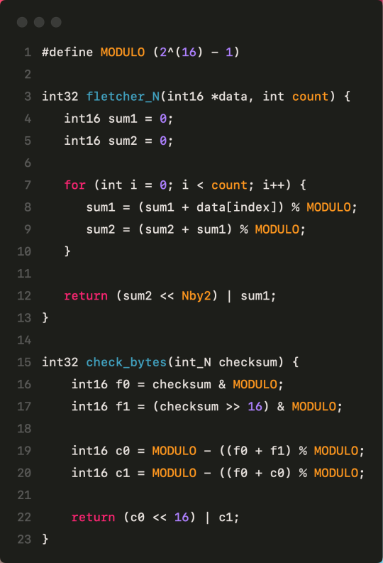
Eventually, I'd like to wrap it in a SPI interface and submit it to TinyTapeout, but for now here's the bare RTL. The most up-to-date code is also available on GitHub:
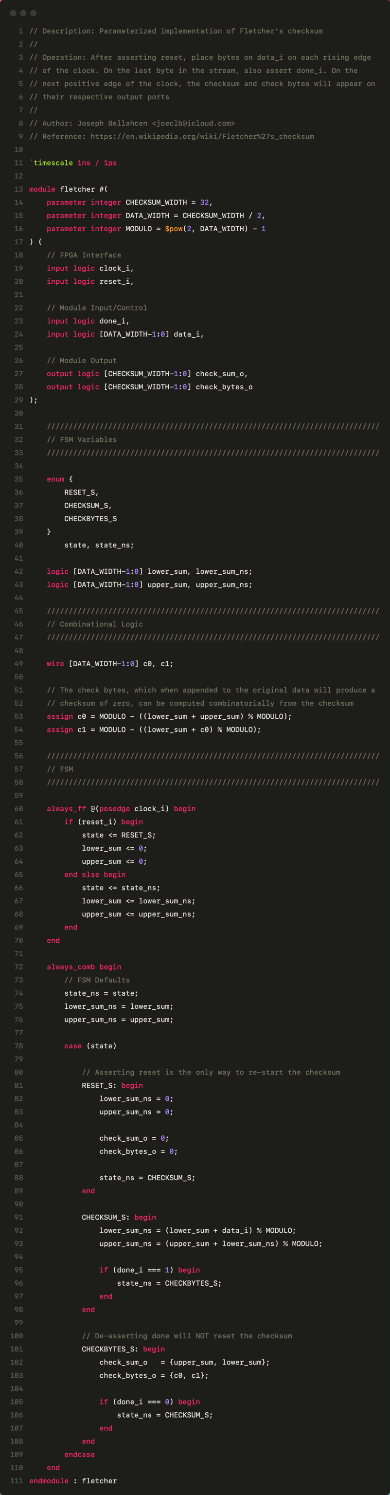
#engineering#computer engineering#fpga#verilog#systemverilog#hardware design#engineering student#studyblr
1 note
·
View note
Text
update:


cant wait to divide in verilog :D this is so easy!
17 notes
·
View notes
Note
ey boss fellow fpga liker here! whats your favourite toolchain?
ayy so sorry I didn't see this a long time ago
tbqh I'm still kinda new to FPGA development, so far I've only ever worked with Lattice FPGAs using Lattice Diamond and their toolchain, which has their own synthesis engine (or you can choose to use Synplify Pro which is included for some reason), and also includes QuestaSim for simulation.
though, I did first start learning verilog using 8bitworkshop.com, they have a great IDE and it's great for beginners, but being a webapp it's RTL simulation only, so you can't even check if the code is even synthesizable.
2 notes
·
View notes
Text
having a day where i just want to give up on literally everything
#i dont want to read about grammar anymore. its boring as fuck and trying to understand how to form a proper sentence#just leads me down this endless void of accusatives and datives and infinitives and transitives and participates and particles and#i come out of it feeling like i learned nothing helpful. and like i have to study this entire other area of stuff#just to even have the *potential* to learn how not to sound like an idiot when i form sentences#i dont want to constantly look up the 73 conjugates every verb has either (and then not be able to find the correct one because i#need to have a master's degree in grammar to understand which one to use!)#I'm also dead tired of this circuits course. All it's done is put some sense into me and convinced me to revert back to my focus on digital#signal processing. I'm no long having any fun with this. I'm also tired of my digital logic class because I'm not interested in building#a new CPU architecture from scratch out of CMOS chips and as a result most of this shit means nothing to me. It's also convinced me that#the advantages of FPGAs are not at all worth the trade-offs compared to microcontrollers. at least not for me.#Verilog is a shitty ass language and Vivado is a shitty ass software#i wanna rip my own head off while doing a backflip
4 notes
·
View notes
Text
youtube
Use this trick to Save time : HDL Simulation through defining clock
Why is this trick useful? Defining a clock in your simulation can save you time during simulation because you don't have to manually generate the clock signal in your simulation environment. Wanted to know how to define and force clock to simulate your digital system. Normally define clock used to simulate system with clock input. But I am telling you this trick for giving values to input ports other than clock. It will help you to save time in simulation because you do not need to force values to input ports every time. Lets brief What we did - gave some clock frequency to input A, like we gave 100. Than we made Half the frequency of clock to 50 and gave it to Input B. In similar way if we have 3rd input too we goanna half the frequency again to 25 and would give to next input.
Subscribe to "Learn And Grow Community"
YouTube : https://www.youtube.com/@LearnAndGrowCommunity
LinkedIn Group : https://www.linkedin.com/groups/7478922/
Blog : https://LearnAndGrowCommunity.blogspot.com/
Facebook : https://www.facebook.com/JoinLearnAndGrowCommunity/
Twitter Handle : https://twitter.com/LNG_Community
DailyMotion : https://www.dailymotion.com/LearnAndGrowCommunity
Instagram Handle : https://www.instagram.com/LearnAndGrowCommunity/
Follow #LearnAndGrowCommunity
#HDL Design#Digital Design#Verilog#VHDL#FPGA#Digital Logic#Project#Simulation#Verification#Synthesis#B.Tech#Engineering#Tutorial#Embedded Systesm#VLSI#Chip Design#Training Courses#Software#Windows#Certification#Career#Hardware Design#Circuit Design#Programming#Electronics Design#ASIC#Xilinx#Altera#Engineering Projects#Engineering Training Program
3 notes
·
View notes
Video
youtube
Implement/Add Multiple Time Delays to 1-bit Signals, RTL Code and Testbe...
1 note
·
View note
Text
That is a very neat idea!
If you like things like that you might want to look into VHDL ( I learned that... some years ago, but have not touched it since ) or Verilog.
They are... programming languages for making logic gate logic.
You combine that with an FPGA, which is essentially a whole lot of NAND gates ( Which as I said, can represent any logic gate system ), and then you can make hardware... via software.
And yes, these essentially do things like your idea. Things that would take a CPU aaaaages to do, can be done very very fast. So you "just" have normal C code, but if it runs onto one of the problems it have hardware for, it uses the hardware.
This is also how graphics cards work, or just floating point operations!
It is insanely cool! :D
What is half-adder and full-adder combinational circuits?
So this question came up in the codeblr discord server, and I thought I would share my answer here too :3
First, a combinational circuit simply means a circuit where the outputs only depends on its input. ( combinational means "Combine" as in, combining the inputs to give some output )
It is a bit like a pure function. It is opposed to circuits like latches which remembers 1 bit. Their output depends on their inputs AND their state.
These circuits can be shown via their logic gates, or truth tables. I will explain using only words and the circuits, but you can look up the truth tablet for each of the circuits I talk about to help understand.

Ok, so an in the case of electronics is a circuit made with logic gates ( I... assume you know what they are... Otherwise ask and I can explain them too ) that adds 2 binary numbers, each which have only 1 character.
So one number is 1 or 0
And the other number is 1 or 0
So the possible outputs are are 0, 1 and 2.
Since you can only express from 0 to 1 with one binary number, and 0 to 3 with 2, we need to output 2 binary numbers to give the answer. So the output is 2 binary numbers
00 = 0
01 = 1
10 = 2
11 = 3 // This can never happen with a half adder. The max possible result is 2
Each character will be represented with a wire, and a wire is a 0 if it is low voltage (usually ground, or 0 volts) and a 1 if it is high voltage (Voltage depends. Can be 5 volts, 3.3, 12 or something else. )
BUT if you only use half adders, you can ONLY add 2 single character binary numbers together. Never more.
If you want to add more together, you need a full adder. This takes 3 single character binary numbers, and adds them and outputs a single 2 character number.
This means it have 3 inputs and 2 outputs.

We have 2 outputs because we need to give a result that is 0, 1, 2 or 3
Same binary as before, except now we CAN get a 11 (which is 3)
And we can chain full adders together to count as many inputs as we want.
So why ever use a half adder? Well, every logic gate cirquit can be made of NAND (Not and) gates, so we usually compare complexity in how many NAND gates it would take to make a circuit. More NAND gates needed means the circuit is slower and more expensive to make.
A half adder takes 5 NAND gates to make
A full adder takes 9 NAND gates.
So only use a full adder if you need one.
Geeks for Geeks have a page for each of the most normal basic cirquits:
I hope that made sense, and was useful :3
41 notes
·
View notes
Text
People who complain about plural teens being annoying about their headmates usually have no idea how annoying can be plurals with a job that they like.
Especially if different headmates have different jobs and help each other at that. It just does not stop.
#actuallyplural#nelke.txt#Oh you cannot handle fandom talk interspersed with plurality?#you will not survive five minutes of headmates conversing about Verilog
2 notes
·
View notes