#VHDL ASIC
Explore tagged Tumblr posts
Visit Tumblr Blog
Explore Tumblr blogs with no restrictions, modern design and the best experience.
Last Seen Tumblr Blogs


Fun Fact
Celebrities use Tumblr as well.
Text
youtube
VHDL Tutorial - Complete Guide to VHDL Process Statement for Beginners [20 mins] [Easy Way]
Welcome to this comprehensive VHDL tutorial where we will dive into the VHDL process statement. In this easy-to-follow guide, we will take you through the syntax and usage of the VHDL process statement, catering especially to beginners. This tutorial will provide you with a thorough understanding of the VHDL process and how it can be effectively implemented in your projects.
Subscribe to "Learn And Grow Community"
YouTube : https://www.youtube.com/@LearnAndGrowCommunity
LinkedIn Group : https://www.linkedin.com/groups/7478922/
Blog : https://LearnAndGrowCommunity.blogspot.com/
Facebook : https://www.facebook.com/JoinLearnAndGrowCommunity/
Twitter Handle : https://twitter.com/LNG_Community
DailyMotion : https://www.dailymotion.com/LearnAndGrowCommunity
Instagram Handle : https://www.instagram.com/LearnAndGrowCommunity/
Follow #LearnAndGrowCommunity
#VHDL tutorial#VHDL process statement#VHDL syntax#VHDL beginner's guide#VHDL tutorial for beginners#VHDL process explained#VHDL process tutorial#VHDL sequential logic#VHDL combinational logic#VHDL development#VHDL design#VHDL FPGA#VHDL ASIC#VHDL circuits#VHDL learning#VHDL education#VHDL digital design#VHDL programming#HDL Design#Digital Design#Verilog#VHDL#FPGA#Simulation#Project#Synthesis#Training#Career#Programming Language#Xilinx
1 note
·
View note
Text
Mastering VLSI: Why the Right Training Matters for a Thriving Tech Career
The Rising Demand for VLSI Experts The modern world is driven by electronics. From smartphones to smart cars, every innovation depends on microchips designed using VLSI (Very Large Scale Integration) technology. With the growing use of AI, IoT, and automation, the need for skilled VLSI professionals has increased rapidly. This makes VLSI an essential field for those looking to build a strong career in electronics and semiconductor industries. Choosing the right learning path is key to making the most of this opportunity.
Exploring the Benefits of VLSI Online Training Courses Many learners today seek flexible and effective ways to upskill. VLSI online training courses offer an excellent solution by combining convenience with quality education. These courses provide access to experienced instructors, practical assignments, and industry-based projects—all from the comfort of home. Learners can grasp digital design, physical design, verification, and ASIC/FPGA concepts without sacrificing their job or academic responsibilities. The online model also allows repeated learning and flexible scheduling, making it ideal for beginners as well as professionals wanting to upgrade their knowledge.
Choosing the Right Learning Mode While online learning provides flexibility, some individuals prefer classroom-based teaching for real-time interaction and immediate doubt clearing. The choice between online and offline modes largely depends on individual preferences, learning habits, and career goals. However, what truly matters is the quality of the training and the expertise of the instructors involved.
Key Skills Taught in VLSI Training A well-structured VLSI course should cover areas like CMOS technology, HDL languages such as Verilog and VHDL, physical design flow, and functional verification techniques. Practical exposure through lab sessions or simulation tools is crucial. Additionally, learners should be guided on real-time projects to apply their theoretical knowledge to industry problems.
Why VLSI Coaching in Hyderabad is Gaining Popularity Hyderabad has become a major hub for semiconductor and electronics industries. As a result, VLSI coaching in Hyderabad has gained recognition for producing skilled professionals. Reputed training centers in the city offer tailored coaching with an industry-aligned curriculum, experienced faculty, and placement support. Many aspirants from across the country travel to Hyderabad to benefit from this coaching environment that bridges academic learning with industry demands.
Conclusion VLSI technology plays a vital role in shaping the electronics and semiconductor industries. Whether through VLSI online training courses or classroom-based programs like VLSI coaching in Hyderabad, acquiring the right skills is essential for career growth. Institutions like Takshila Institute of VLSI Technologies provide training that matches industry standards, helping learners succeed in a competitive field. The choice of platform and location may differ, but the goal remains the same—building a strong foundation in VLSI for a successful future.
0 notes
Text
Mastering the Future of Chip Design: Explore ASIC Training from Anywhere
The Rising Relevance of ASIC Design in the Semiconductor Industry
In today’s tech-driven world, Application-Specific Integrated Circuits (ASICs) play a pivotal role in shaping electronic innovations. From smartphones and medical devices to artificial intelligence and automotive electronics, ASICs are embedded in almost every aspect of modern technology. As industries evolve, the demand for engineers skilled in ASIC design continues to surge. This increasing demand has created a clear path for aspiring VLSI professionals to seek specialized training that aligns with industry needs.
Why Online ASIC Design Training is the Smart Choice
The convenience and flexibility of learning from home have led to the growing popularity of online asic design training programs. These virtual platforms provide comprehensive learning modules that allow learners to gain hands-on experience without the limitations of geographical boundaries. Whether someone is a recent engineering graduate or an industry professional looking to upskill, these online programs make it easier to access quality education at one's own pace. With the use of simulation tools, video lectures, and live project support, learners receive training that is practical, relevant, and industry-focused.
Essential Skills Gained Through ASIC Training
ASIC design is a multifaceted field that combines knowledge of digital electronics, hardware description languages, verification methodologies, and physical design principles. A well-structured training program ensures that learners become proficient in tools such as Verilog, VHDL, Synopsys, and Cadence. It also fosters a strong understanding of timing analysis, synthesis, and low-power design techniques. These are essential competencies for engineers working in semiconductor and VLSI companies.
Hyderabad – A Growing Hub for ASIC Training Excellence
Hyderabad has become a prominent location for VLSI and semiconductor training, offering access to some of the finest educational resources in India. Several online asic design training institutes in hyderabad have emerged as reliable options for those aiming to build a career in chip design. These institutes not only provide technical guidance but also offer placement support, industry interaction, and live project exposure. Hyderabad’s growing ecosystem of VLSI companies further boosts the scope for real-world learning and employment opportunities.
Conclusion: Finding the Right Training Path in a Digital World
To thrive in the evolving semiconductor industry, quality education in ASIC design is indispensable. Choosing the right training platform can make a lasting impact on a learner’s professional journey. That’s why institutes like Takshila Institute of VLSI Technologies have become trusted names for those looking to gain advanced skills in VLSI. With its industry-aligned curriculum and online accessibility, it bridges the gap between academic learning and professional excellence.
Whether opting for online asic design training or exploring online asic design training institutes in hyderabad, the goal remains the same: to master the art of designing the future’s most critical hardware components.
0 notes
Text
Job-Oriented Online VLSI Training at Takshila Institute of VLSI Technologies in India
In today’s fast-paced digital world, the demand for skilled VLSI (Very Large Scale Integration) engineers is growing rapidly. To meet this demand, many engineering graduates and professionals are turning to online VLSI training institutes for flexible, high-quality education. One of the leading institutes in India offering job-oriented VLSI training is the Takshila Institute of VLSI Technologies. Known for its industry-focused approach and practical training methods, Takshila provides an excellent platform for individuals seeking to build a successful career in the VLSI domain.
Why Choose Takshila Institute of VLSI Technologies The Takshila Institute of VLSI Technologies has established itself as a top choice among online learners across India. The institute offers specially designed online VLSI training programs that are structured to match industry needs and current job requirements. Whether you are a fresh graduate or a working professional looking to upgrade your skills, Takshila’s training modules provide the right mix of theory and hands-on practice.
One of the standout features of Takshila’s programs is their strong focus on job oriented VLSI training. The courses are carefully crafted by industry experts to cover all essential areas such as digital design, Verilog, VHDL, CMOS fundamentals, physical design, and ASIC verification. In addition, students get to work on real-time projects and tools used in the semiconductor industry.
Flexible and Practical Learning Takshila’s online VLSI training courses offer the flexibility to learn from anywhere in India without compromising on quality. The training includes live instructor-led sessions, recorded video lectures, assignments, and regular assessments to ensure continuous learning. The institute also offers one-on-one mentoring and guidance, which helps students strengthen their concepts and prepare for interviews.
Placement-Focused Training What sets Takshila apart from other online VLSI training institutes is its strong commitment to student placement. The institute has a dedicated placement team that supports students with resume building, mock interviews, and job referrals. With a strong network of industry connections, Takshila has helped many students secure positions in top semiconductor companies across India.
Conclusion For those seeking quality online VLSI training that is both flexible and career-focused, the Takshila Institute of VLSI Technologies in India offers an ideal solution. With its job-oriented VLSI training programs, expert faculty, and solid placement support, Takshila empowers students to gain the skills needed to thrive in the competitive VLSI industry.
0 notes
Text

Join the Best VLSI Course in Tirupati – Upgrade Your Career in Chip Design
A valid opportunity for anyone wanting to build a career in the semiconductor industry. Come, enrol in the best VLSI course up for grabs in Tirupati, for students and professionals striving to become experts in VLSI Design, Verification, and FPGA Implementation. The program teaches Digital Design, Verilog HDL, ASIC, VHDL, and many more relevant topics for making you fit for a job in leading tech companies.
We provide basic internship, real-time projects, and professional mentoring at the core of Tirupati for practical exposure. Designed for CSE, ECE, or EEE students, this course is tuned to give you a competitive edge in the fast-growing VLSI industry.
Students are guided at a project level in VLSI by Takeoffupskill, which best suits students in their last year of B.Tech or M.Tech. We are the very first in Tirupati to be an overall analytical and lab-on type ground for training VLSI.
#VLSICourse#VLSITraining#VLSIDesign#VLSIEngineering#ASICDesign#FPGAProgramming#ChipDesign#SemiconductorTraining#DigitalElectronics#HardwareDesign#TakeoffEduGroup#takeoffupskill
0 notes
Text
Master ASIC Design and Verification Training Today

In today’s fast-paced semiconductor industry, mastering ASIC (Application-Specific Integrated Circuit) design and verification is essential for engineers and professionals looking to advance their careers. With cutting-edge technology and increasing demand for customized chip designs, the need for skilled ASIC designers is greater than ever. If you are eager to enhance your expertise, ASIC Design and Verification Training is the perfect opportunity to gain in-depth knowledge and practical skills.
Why Choose ASIC Design and Verification Training?
ASIC design is a complex yet rewarding field that requires a deep understanding of digital circuits, system architecture, and verification methodologies. This training equips you with:
Fundamental and Advanced ASIC Design Concepts – Learn the principles of ASIC development, from design to implementation.
Verification Techniques – Master simulation-based verification, formal verification, and functional testing.
Industry-Standard Tools – Get hands-on experience with tools like Verilog, VHDL, SystemVerilog, and UVM.
Practical Projects and Case Studies – Work on real-world projects to strengthen your problem-solving abilities.
Expert Guidance – Learn from industry professionals with years of experience in ASIC design and verification.
Who Should Enroll?
This training is ideal for:
Engineering students and graduates looking to specialize in VLSI and ASIC design.
Working professionals aiming to upskill in semiconductor design.
Anyone passionate about learning digital design and verification methodologies.
Career Benefits of ASIC Design and Verification Online Training
With expertise in ASIC design and verification, you can unlock various career opportunities in semiconductor and electronics industries. Job roles include:
ASIC Design Engineer
Verification Engineer
FPGA Engineer
VLSI Design Engineer
Embedded Systems Engineer
Enroll Today and Advance Your Career!
Don’t miss the chance to boost your career in the high-demand field of ASIC design. Join ASIC Design and Verification Training today and gain the skills needed to thrive in the semiconductor industry. Start your journey towards success with expert-led training and hands-on experience.
At Multisoft Virtual Academy, we provide comprehensive training programs to help tech enthusiasts achieve professional excellence. Sign up now and take the next step in your career!
0 notes
Text
ASIC Design of Complex Multiplier: A Comprehensive Overview

In the modern era of digital signal processing (DSP) and communication systems, multipliers play a pivotal role. Complex multipliers, in particular, are essential in a wide array of applications such as Fast Fourier Transforms (FFT), Digital Down Converters (DDC), and MIMO communication systems. The design of an Application-Specific Integrated Circuit (ASIC) for a complex multiplier presents unique challenges and opportunities. In this blog, we delve into the intricacies of ASIC design for complex multipliers, exploring their architecture, design methodologies, and optimization techniques.
What is a Complex Multiplier?
A complex multiplier is a circuit that performs multiplication of two complex numbers. Mathematically, if and are two complex numbers, their product is given by:
This equation shows that a complex multiplier requires four real multiplications and two real additions/subtractions.
Key Considerations in ASIC Design of Complex Multipliers
Area Efficiency: ASIC designs often operate under strict area constraints. Optimizing the layout and minimizing the number of logic gates are crucial for reducing silicon area.
Power Consumption: Power efficiency is paramount, especially for portable or battery-operated devices. Techniques like clock gating, operand isolation, and optimized arithmetic circuits help in reducing dynamic and static power consumption.
Speed: High-speed operation is critical for real-time applications. The multiplier design must ensure minimal propagation delay while maintaining accuracy.
Precision: Depending on the application, the design may require fixed-point or floating-point arithmetic, which significantly impacts complexity and performance.
Process Technology: The choice of CMOS technology node (e.g., 28nm, 14nm, etc.) influences performance, power, and area (PPA) trade-offs.
Architecture of a Complex Multiplier
A typical complex multiplier architecture consists of the following components:
Four Real Multipliers: These are the core computation units.
Two Adders/Subtractors: These units perform the addition and subtraction of intermediate results.
Pipeline Registers (Optional): Pipelining enhances throughput by reducing the critical path.
To optimize the design, advanced techniques such as Booth encoding, Wallace tree structures, or Distributed Arithmetic (DA) can be employed for the real multipliers.
Design Methodology
Behavioral Modeling: The initial design begins with a high-level behavioral model in languages like VHDL or Verilog.
Synthesis: The behavioral model is synthesized into a gate-level netlist using ASIC synthesis tools like Synopsys Design Compiler.
Place and Route (P&R): The synthesized netlist is mapped to physical silicon, ensuring minimal area and optimal routing.
Timing Analysis: Static Timing Analysis (STA) is conducted to ensure the design meets timing constraints.
Power Analysis: Tools like PrimePower are used to estimate dynamic and leakage power.
Verification: Functional and formal verification ensure the design adheres to the specification.
Optimization Techniques
Shared Multipliers: Sharing multiplier resources between multiple computations can significantly reduce area and power.
Approximate Computing: For applications tolerant to small errors, approximate multipliers can be used to save power and area.
Parallel Processing: Increasing parallelism can improve throughput but must be balanced against area and power constraints.
Custom Arithmetic Units: Designing custom arithmetic circuits tailored to specific applications can yield significant gains in efficiency.
Challenges in ASIC Design
Design Complexity: Managing trade-offs between speed, power, and area is challenging, particularly in advanced nodes.
Process Variability: Variations in the manufacturing process can impact performance and yield.
Integration: The multiplier must seamlessly integrate with other blocks in the ASIC.
Applications of Complex Multipliers
Signal Processing: Used in FFTs, FIR filters, and spectral analysis.
Wireless Communication: Essential for modulation and demodulation tasks.
Image Processing: Facilitates convolution and correlation operations.
Cryptography: Key component in algorithms like RSA and ECC.
Conclusion
The ASIC design of a complex multiplier is a multifaceted process requiring careful consideration of performance, power, and area trade-offs. With advancements in process technology and design tools, engineers can achieve highly efficient designs tailored to specific applications. By leveraging optimization techniques and innovative architectures, complex multipliers can continue to meet the growing demands of modern DSP and communication systems.
Whether you're a seasoned ASIC designer or a budding engineer, the design of a complex multiplier offers an exciting opportunity to push the boundaries of silicon design and computational efficiency.
#Top Most ASIC companies in India#Famous ASIC companies in Bengaluru#Best ASIC companies in USA#Most Famous companies in Hyderabad
0 notes
Text
Hardware Reconfigurable Devices
Hardware reconfigurable devices, such as Field-Programmable Gate Arrays (FPGAs) and Complex Programmable Logic Devices (CPLDs), enable dynamic customization of hardware functionality. Unlike traditional Application-Specific Integrated Circuits (ASICs), which have fixed designs, reconfigurable devices can be programmed to perform a wide range of tasks post-manufacturing. This flexibility is achieved through programmable logic blocks and interconnects.
FPGAs are particularly powerful, offering high parallelism and configurability for tasks such as digital signal processing, artificial intelligence, and cryptography. They excel in applications requiring low latency, real-time processing, or iterative prototyping. In contrast, CPLDs are simpler and used for control-oriented applications like glue logic or signal routing.
Reconfigurable hardware combines the performance of hardware solutions with the adaptability of software. Designs are typically implemented using hardware description languages (HDLs) like VHDL or Verilog and can be updated as requirements evolve.
These devices are widely used in industries such as telecommunications, automotive, and aerospace, where they provide a cost-effective solution to meet changing standards or improve system performance. Advances in tools and technologies continue to enhance their usability, enabling faster deployment of custom hardware solutions.
For More : https://tinyurl.com/u3r79skd

0 notes
Text
VLSI Design And Verification Course For Fresher - VLSI Guru
In the fast-paced world of technology, the VLSI (Very Large Scale Integration) domain stands as a cornerstone for innovations in electronics and semiconductor design. If you’re a fresher aiming to dive into this exciting field, the VLSI Design and Verification Course by VLSI Guru is your perfect launchpad.

Why Choose VLSI as a Career Path?
The demand for skilled professionals in VLSI design and verification is skyrocketing, with industries relying on advanced ASIC (Application-Specific Integrated Circuits) and FPGA (Field-Programmable Gate Arrays) to power cutting-edge technologies. From smartphones to autonomous vehicles, the scope of VLSI is vast and evolving.
What Does the Course Offer?
The VLSI Design and Verification Course by VLSI Guru is tailored for freshers, focusing on:
HDL Languages: Master Verilog and VHDL for RTL coding.
SystemVerilog & UVM: Learn modern verification methodologies for building robust testbenches.
ASIC Design Flow: Gain insights into the complete chip design process.
FPGA Prototyping: Get hands-on experience with FPGA tools and workflows.
Debugging & Tools Expertise: Work with industry-standard tools like Cadence, Synopsys, and Mentor Graphics.
Why VLSI Guru?
VLSI Guru emphasizes practical learning through real-world projects and labs. Freshers are trained to handle challenges in semiconductor design and verification, bridging the gap between academia and industry.
Who Can Enroll?
The course is ideal for engineering graduates in ECE, EE, or CSE with a passion for chip design and a desire to work in leading semiconductor companies.
Start your journey in the semiconductor industry today with VLSI Guru's specialized training.
0 notes
Text
Digital Design and Verification is a crucial process in the development of digital systems, such as integrated circuits (ICs) and electronic devices. It involves several steps to ensure that a design meets its intended functionality, performance, and reliability standards.
Here's a brief overview:
Design Phase: This is where the initial concept is transformed into a detailed design. It often involves creating high-level functional descriptions using Hardware Description Languages (HDLs) like Verilog or VHDL.
Verification Phase: This step ensures that the design meets its specifications. Verification techniques include:
Simulation: Running test cases to check if the design behaves as expected.
Formal Verification: Using mathematical methods to prove that certain properties hold for the design.
Assertion-Based Verification: Checking specific properties or conditions within the design during simulation.
Synthesis: Converting the HDL design into a gate-level representation that can be implemented on hardware like FPGAs or ASICs.
Implementation: The synthesized design is then implemented on the target hardware, and further tests are conducted to ensure it works correctly in the real world.
Would you like to know more about any specific aspect of digital design and verification?
1 note
·
View note
Text
youtube
VHDL Basics : Begin the World of FPGA Design Tools & VHDL Design Flow
Welcome to our comprehensive guide on FPGA design tools and VHDL design flow! In this video, we dive into the fascinating world of FPGA design and explore the essential tools and methodologies needed for successful FPGA development. Whether you're a beginner or an experienced engineer, this tutorial will provide valuable insights and tips to enhance your FPGA design skills. We start by introducing the fundamentals of FPGA design, explaining the benefits and versatility of using FPGAs in various applications. From there, we explore the wide range of design tools available, from popular industry-standard software like Xilinx Vivado and Altera Quartus Prime to open-source alternatives like GHDL and Icarus Verilog. We highlight the strengths and features of each toolset, enabling you to choose the most suitable one for your projects. With a solid foundation in FPGA design and tools, we then delve into the VHDL (VHSIC Hardware Description Language) design flow. From understanding the basics of VHDL syntax to implementing complex digital designs, we provide step-by-step explanations and practical demonstrations. You'll learn about entity and architecture design, the importance of libraries, and how to simulate and synthesize VHDL code for your FPGA. To ensure a holistic learning experience, we discuss common challenges and pitfalls in FPGA design and provide valuable troubleshooting tips. We also touch upon advanced topics like FPGA optimization techniques, timing analysis, and physical implementation considerations. So, whether you're a student, hobbyist, or professional looking to enhance your FPGA design skills, this tutorial is the ultimate resource to get started on your journey. Join us now and unlock the vast potential of FPGA design tools and the VHDL design flow! FPGA design tools, VHDL design flow, FPGA development, Xilinx Vivado, Altera Quartus Prime, VHDL, Verilog, VHDL syntax, digital design, entity architecture, libraries, simulate VHDL code, synthesize VHDL code, FPGA optimization techniques, timing analysis, physical implementation, FPGA design skills.
Subscribe to "Learn And Grow Community"
YouTube : https://www.youtube.com/@LearnAndGrowCommunity
LinkedIn Group : https://www.linkedin.com/groups/7478922/
Blog : https://LearnAndGrowCommunity.blogspot.com/
Facebook : https://www.facebook.com/JoinLearnAndGrowCommunity/
Twitter Handle : https://twitter.com/LNG_Community
DailyMotion : https://www.dailymotion.com/LearnAndGrowCommunity
Instagram Handle : https://www.instagram.com/LearnAndGrowCommunity/
Follow #LearnAndGrowCommunity
#HDL Design#Digital Design#Verilog#VHDL#FPGA#Simulation#Synthesis#B.Tech#VLSI#Training#Career#ASIC#Xilinx#Students#hardware description language#VHDL tutorial#VHDL beginner guide#VHDL syntax#VHDL data types#VHDL modeling#behavioral modeling#data flow modeling#FSM#FPGA design tools#VHDL design flow#FPGA development#Xilinx Vivado#Altera Quartus Prime#entity#architecture
1 note
·
View note
Text
Paving the Path to VLSI Success: A Deep Dive into Learning Opportunities
The Rising Demand for VLSI Professionals
In today’s technology-driven world, the demand for skilled professionals in the field of Very-Large-Scale Integration (VLSI) continues to surge. VLSI technology forms the foundation of most modern electronic devices, from smartphones to satellites. As integrated circuits become more complex, the need for engineers who can design, test, and improve these systems grows. Engineering students and electronics graduates looking to future-proof their careers are increasingly drawn to VLSI as a specialization. Companies in India and around the world are on the lookout for talent equipped with practical VLSI skills, making this an attractive career path. Given this scenario, educational institutions and private training centers have stepped up to provide in-depth programs designed to meet industry needs. Aspiring engineers now have a variety of options to choose from when selecting the right program to build their foundation in VLSI technology.
Importance of Industry-Relevant Training in VLSI
While a formal degree in electronics or electrical engineering provides the basics, industry-relevant training in VLSI is critical for practical success. This is because VLSI is highly application-based, demanding a strong understanding of design tools, programming languages, and testing methodologies. Hands-on experience with CAD tools, simulation software, and real-time projects can make all the difference. As a result, the choice of a training institute becomes an important factor. Students looking to enter this domain often search for the top vlsi institutes in hyderabad, as Hyderabad is a major technology hub with several reputed centers offering quality training. These institutes focus on practical exposure, experienced faculty, and placement support, all of which are key to student success. With proper guidance and the right learning environment, students can gain the skills required to thrive in this competitive field.
Choosing the Right VLSI Course
Selecting the right VLSI course is essential for aligning one's career goals with market expectations. The ideal course not only covers theoretical knowledge but also emphasizes real-world application. Curriculum components typically include digital design, CMOS technology, Verilog/VHDL, ASIC design, and FPGA implementation. Additionally, courses offering modules on SystemVerilog, UVM, and embedded systems are becoming increasingly popular. When evaluating course offerings, many prospective students explore vlsi courses in hyderabad to find a comprehensive program that covers both front-end and back-end design processes. It is important for learners to also consider the duration, mode of delivery (online/offline), and availability of project work. A structured course with industry-certified trainers and access to advanced lab setups can provide a valuable edge in this field. This clarity helps learners not only gain knowledge but also build a strong portfolio that can appeal to future employers.
Placement Support and Career Opportunities
One of the biggest advantages of enrolling in a reputed VLSI training program is the access to placement support. Leading institutes often have tie-ups with semiconductor companies, startups, and multinational corporations looking for trained professionals. Career opportunities in VLSI are vast, ranging from physical design engineers to verification specialists and DFT engineers. With the growth of IoT, AI, and 5G technologies, VLSI engineers are finding exciting roles in hardware development teams across domains. Institutes that focus on industry connections, mock interviews, resume building, and internships significantly boost a student’s employability. Moreover, alumni networks and mentorship programs help learners stay updated on trends and job openings. A combination of technical skills and soft skills training can greatly improve the likelihood of landing a dream role. As the semiconductor industry continues to grow, so too does the demand for qualified, hands-on VLSI professionals.
Conclusion: Begin Your VLSI Journey with Confidence
Choosing the right institute and course is the first step toward a successful VLSI career. From understanding the fundamentals to mastering design and verification tools, a structured training program can be a game changer. Whether you're a fresh graduate or a working professional looking to switch domains, VLSI offers a dynamic and rewarding path. Hyderabad, as a tech hub, continues to provide ample opportunities for learning and growth in this field. Institutes that combine practical training, expert mentorship, and placement assistance can help bridge the gap between education and employment. If you're looking to start or elevate your career in this domain, takshila-vlsi.com is a reliable place to begin your journey.
0 notes
Text
Online VLSI Training Institutes and VLSI Training at Takshila Institute of VLSI Technologies
The Takshila Institute of VLSI Technologies in India is a premier institute offering specialized VLSI training for students and professionals who want to build a career in the semiconductor industry. As the demand for skilled VLSI engineers continues to grow, the institute provides high-quality training through both classroom and online learning programs.
For those looking for flexible learning options, the Takshila Institute of VLSI Technologies is among the top online VLSI training institutes, offering comprehensive courses in digital design, ASIC, FPGA, verification, and physical design. The online VLSI training is designed to provide an industry-oriented learning experience through live interactive sessions, recorded lectures, hands-on projects, and mentorship from industry experts. Students gain practical exposure to EDA tools and design methodologies, ensuring they are well-prepared for real-world challenges.
The institute also provides VLSI training through its structured classroom programs, where students can gain in-depth knowledge of RTL design, ASIC verification, physical design, and custom layout. The courses cover key topics such as Verilog, VHDL, synthesis, timing analysis, DFT, and semiconductor fabrication. With expert faculty and access to state-of-the-art lab facilities, students get hands-on experience with industry-standard workflows.
One of the key advantages of enrolling in VLSI training at Takshila Institute of VLSI Technologies is the placement support provided to students. The training aligns with industry requirements, ensuring that graduates are well-prepared for job opportunities in VLSI design, verification, and testing. Many students have successfully secured positions in leading semiconductor companies after completing their training.
With a strong curriculum, hands-on training, and expert mentorship, the Takshila Institute of VLSI Technologies stands out as one of the best VLSI training institutes in India. Whether you choose online or classroom-based training, these programs offer an excellent opportunity to build a successful career in VLSI and semiconductor technology.
0 notes
Text
Learning ASIC Design Online to Advance a Rewarding Career
The need for qualified ASIC (Application-Specific Integrated Circuit) designers has skyrocketed in line with the fast technological changes. Designed to satisfy individuals driven to succeed in electronics and embedded systems, an ASIC design course provides a portal into the fascinating field of custom chip design. Unlike general-purpose integrated circuits, ASICs are specialist circuits tailored for a certain application. From consumer electronics to healthcare and automotive, these chips are very essential in devices of many kinds. Learning ASIC design gives engineers the technical tools they need to create customized solutions, hence providing interesting career routes in sectors in demand.
Essential Learning Materials for an ASIC Design Course
Usually covering both basic and advanced subjects, an ASIC design course combines theory with useful design methods. Starting with the foundations of digital design, students next explore hardware description languages (HDLs) such as Verilog and VHDL, which are important for specifying circuit behavior. To guarantee circuits satisfy high-performance criteria, the course moves through logic synthesis, functional verification, and timing analysis. Emphasizing practical laboratories, students get real-world experience working with instruments of industrial standard. This extensive course guarantees that students grasp the design process completely, therefore equipping them for the demanding requirements of ASIC development employment.
Online ASIC Design Training's advantages
Online ASIC design training has made it simpler than ever in recent years to gain these specialist abilities free from geographical restrictions. Online courses let students and professionals study at their speed by offering flexible scheduling. These classes are meant to fit working professionals, students, and even amateurs hoping to become ASIC designers. Online training offers a collaborative learning environment using interactive modules, live sessions, and forums. Expert advice and peer conversations help students create a dynamic environment that replicates real-world situations while keeping flexibility for their hectic lives.
Employment Prospectives and Professional Development Using ASIC Design Skills
Demand for ASIC designers is strong in many areas, but especially in tech-driven sectors such as IoT, 5G, and artificial intelligence. Businesses always want talented ASIC designers to provide effective, small-sized, high-performance processors. Completing an ASIC design course lets professionals work as physical design experts, verification engineers, and ASIC design engineers with employment paying attractive rates and opportunities for career development. Furthermore, given the growing complexity of digital goods, ASIC knowledge of new technologies is always in demand, so this ability is not only useful but also future-proof in a sector that is always changing.
Selecting the Correct Platform for ASIC Design Education
Achieving one's professional objectives depends on choosing the right platform to learn ASIC design. Prospective students should search for courses offering a theoretical background as well as real-world industry tool experience like Cadence, Synopsys, and Mentor Graphics. The learning process may be improved with thorough assistance via digital laboratories, lecture recordings, and Q&A sessions, among other online tools. Many online ASIC design training courses include certificates that enhance a candidate's profile and provide credibility, therefore helping them stand out to companies in a crowded employment market. Selecting a respectable course guarantees students' readiness for the expectations of the sector.
Conclusion
Following an ASIC design course—especially via online resources—opens a world of possibilities in integrated circuit design. Those with specific expertise and useful abilities may boldly join the market in fields dependent on high-performance, customized chips. For novices as well as seasoned experts, the adaptability of online ASIC design training lets students acquire industry-relevant knowledge from anywhere. Platforms like takshila-vlsi.com provide priceless training materials for people wanting to improve their VLSI abilities and flourish in ASIC design, therefore bridging the knowledge gap between expertise required in today's tech scene.
0 notes
Text
FPGA vs Microcontroller: The Ultimate Programmable Showdown

FPGA vs Microcontroller
Two types of integrated circuits (ICs) that are frequently contrasted are field programmable gate arrays (FPGAs) and microcontroller units (MCUs). Embedded systems and digital design are two typical applications for these ICs. It is possible to think of FPGA vs microcontroller as “small computers” that may be included into smaller gadgets and bigger systems.
Programmability and processing power are the main distinctions between FPGA and microcontroller as processors. FPGAs are more costly even though they have greater power and versatility. Microcontrollers are less expensive, but they also offer less customisation. Microcontrollers are quite powerful and affordable in many applications. Nonetheless, FPGAs are required for some demanding or evolving applications, such as those that need parallel processing.
FPGAs have hardware reprogrammability, in contrast to microcontrollers. Because of their distinctive design, users are able to alter the chip’s architecture to suit the needs of the application. Microcontrollers can only read one line of code, but FPGAs can handle many inputs. An FPGA can be programmed like a microcontroller, but not vice versa.
The FPGA is field-programmable gate array
FPGAs from Xilinx debuted in 1985. Processing power and adaptability are their hallmarks. Therefore, they are recommended for many DSP, prototyping, and HPC applications.
FPGAs, unlike ASICs, can be customised and reconfigured “in the field,” after production. FPGAs’ primary feature is customisation, but they also require programmability. FPGAs must be configured in verilog or VHDL, unlike ASICs. Programming an FPGA requires expertise, which increases costs and delays adoption. Generally, FPGAs need to be set upon startup, however some do have non-volatile memory that can save programming instructions after the device is turned down.
FPGA advantages
FPGAs are nonetheless helpful in applications that demand high performance, low latency, and real-time adaptability in spite of these difficulties. FPGAs work especially effectively in applications that need the following:
Quick prototyping
FPGAs may be readily configured into a variety of customised digital circuit types, avoiding the need for expensive and time-consuming fabrication processes and enabling faster deployments, evaluations, and modifications.
Hardware-based accelerated
The FPGA’s parallel processing capabilities are advantageous for demanding applications. For computationally demanding applications like machine learning algorithms, cryptography, and signal processing, FPGAs may provide considerable performance gains.
Personalisation
FPGAs are a versatile hardware option that are simple to customise to fit the demands of a given project.
Durability
Given that FPGAs may be updated and modified to meet changing project demands and technology standards, FPGA-based designs may have a longer hardware lifecycle.
FPGA parts
FPGAs are made up of a variety of programmable logic units connected by a programmable routing fabric in order to provide reconfigurability. The following are the key parts of a standard FPGA:
Blocks of configurable logic (CLBs)
In addition to providing computation capabilities, CLBs may have a limited number of simple logic components, including flip-flops for data storage, multiplexors, logic gates, and small look-up tables (LUTs).
Interconnects with programming capabilities
These linkages, which consist of wire segments connected by electrically programmable switches, offer routing channels between the various FPGA resources, enabling the development of unique digital circuits and a variety of topologies.
Blocks for I/O (IOBs)
Input output (I/O) blocks facilitate the interaction between an FPGA and other external devices by enabling the FPGA to receive data from and operate peripherals.
FPGA applications
Due to its versatility, FPGAs are used in many industries.
Aerospace and defence
FPGAs are the ideal option for image processing, secure communications, radar systems, and radar systems because they provide high-speed parallel processing that is useful for data collecting.
Systems of industrial control (ICS)
Power grids, oil refineries, and water treatment plants are just a few examples of the industrial control systems that use FPGAs, which are easily optimised to match the specific requirements of different industries. FPGAs can be utilised to create several automations and hardware-based encryption features for effective cybersecurity in these vital industries.
ASIC creation
New ASIC chips are frequently prototyped using FPGAs.
Automotive
FPGAs are ideally suited for advanced driving assistance systems (ADAS), sensor fusion, and GPS due to their sophisticated signal processing capabilities.
Information hubs
By optimising high-bandwidth, low-latency servers, networking, and storage infrastructure, FPGAs enhance the value of data centres.
Features of FPGAs
Processor core: Logic blocks that can be configured
Memory: Interface for external memory
auxiliary parts: Modifiable input/output blocks
Programming: Hardware description language (VHDL, Verilog) is used in programming.
Reconfigurability: Extremely reprogrammable and reconfigurable logic
What is a microcontroller?
Microcontrollers are a kind of small, pre-assembled ASIC that have an erasable programmable read-only memory (EPROM) for storing bespoke programmes, memory (RAM), and a processor core (or cores). Microcontrollers, sometimes referred to as “system-on-a-chip (SoC)” solutions, are essentially tiny computers combined into a single piece of hardware that may be utilised separately or in larger embedded systems.
Because of their affordable accessibility, hobbyists and educators prefer consumer-grade microcontrollers, including the Arduino Starter Kit and Microchip Technology PIC, which can be customised using assembly language or mainstream programming languages (C, C++). Microcontrollers are frequently used in industrial applications and are also capable of managing increasingly difficult and important jobs. However, in more demanding applications, a microcontroller’s effectiveness may be limited by reduced processing power and memory resources.
Benefits of microcontrollers
Microcontrollers have numerous benefits despite their drawbacks, such as the following:
Small-scale layout
Microcontrollers combine all required parts onto a single, compact chip, making them useful in applications where weight and size are important considerations.
Energy effectiveness
Because they utilise little power, microcontrollers are perfect for battery-powered gadgets and other power-constrained applications.
Economical
By delivering a full SoC solution, microcontrollers reduce peripheral needs.All-purpose, low-cost microcontrollers can significantly cut project costs.
Adaptability
While less flexible than FPGA and microcontroller can be programmed for many applications. Software can change, update, and tune microcontrollers, but hardware cannot.
Parts of microcontrollers
Compact and capable, self-contained microcontrollers are an excellent option when reprogrammability is not a top concern. The essential parts of a microcontroller are as follows:
CPU, or central processing unit
The CPU, sometimes known as the “brain,” executes commands and manages processes.
Recall
Non-volatile memory (ROM, FLASH) stores the microcontroller’s programming code, while volatile memory (RAM) stores temporary data that could be lost if the system loses power.
Auxiliary
Depending on the application, a microcontroller may have communication protocols (UART, SPI, I2C) and I/O interfaces like timers, counters, and ADCs.
Use cases for microcontrollers
Small, inexpensive, and non-volatile microcontrollers, in contrast to FPGAs, are widely used in contemporary electronics and are typically employed for certain purposes, such as the following:
Vehicle systems
Airbag deployment, engine control, and in-car infotainment systems all require microcontrollers.
End-user devices
Smartphones, smart TVs, and other household appliances especially IoT-connected ones use microcontrollers.
Automation in industry
Industrial applications include process automation, machinery control, and system monitoring are ideal uses for microcontrollers.
Medical equipment
Microcontrollers are frequently used in life-saving equipment including blood glucose monitors, pacemakers, and diagnostic instruments.
Features of a microcontroller
Central processing unit: Unchanged CPU Memory: ROM/Flash and integrated RAM Auxiliary parts: Integrated I/O interfaces for Software (C, Assembly) Programming Limited reconfigurability; firmware upgrades
Important distinctions between microcontrollers and FPGAs
A number of significant distinctions between FPGA and microcontroller should be taken into account when comparing them, including developer requirements, hardware architecture, processing power, and capabilities.
Hardware configuration
FPGA: Easy-to-customize programmable logic blocks and interconnects for digital circuits. Microcontroller: A fixed-architecture microcontroller contains a CPU, memory, and peripherals.
Capabilities for processing
FPGA: Multiple simultaneous processes are made possible by advanced parallel processing. Microcontroller: Capable of handling only one instruction at a time, microcontrollers are made for sequential processing.
Power usage
FPGA: Power consumption is usually higher than that of microcontrollers. Microcontroller: Designed to use less power, ideal for applications that run on batteries.
Coding
FPGA: Configuring and debugging this device requires specific understanding of hardware description languages. Microcontroller: Software development languages such as Javascript, Python, C, C++, and assembly languages can be used to programming microcontrollers.
Price
FPGA: FPGA hardware offers more power but comes with a higher price tag due to its higher power consumption and need for specialised programming abilities. It also requires advanced expertise. Microcontroller: Typically, a less expensive option that is readily available off the shelf, uses less power, and supports more widely used programming languages.
Flexibility
FPGA: Compared to microcontrollers, FPGAs are much more flexible and enable hardware customisation. Microcontroller: Compared to FPGAs, microcontrollers only provide surface-level customisation, despite being well-suited for a wide range of applications.
Examine the infrastructure solutions offered by IBM
Whether you’re searching for a small, affordable microcontroller or a flexible, potent FPGA processor, think about how IBM’s cutting-edge infrastructure solutions may help you grow your company. The new IBM FlashSystem 5300 offers enhanced cyber-resilience and performance. New IBM Storage Assurance makes storage ownership easier and supports you in resolving IT lifecycle issues.
Read more on Govindhtech.com
#microcontroller#digitaldesign#hardware#HPCapplications#cryptography#datastorage#cybersecurity#cpu#smartphones#Softwaredevelopment#news#technews#technology#technologynews#technologytrends#govindhtech
0 notes
Text
NO.1 VLSI System Design in India
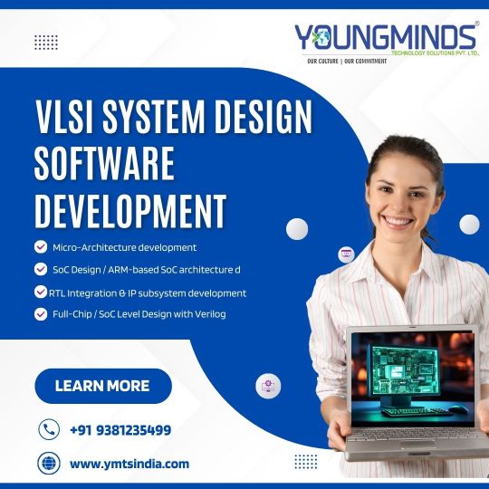
Welcome to Youngminds Technology Solutions, a leading VLSI System Design Software Development Agency in India. Our focus is on the development of the latest solutions that promote innovation and efficiency in the area of VLSI system design. Come with us as we are building the future of technology together.
Our VLSI design team has deep expertise in realizing product and software development for a wide range of application areas on cutting-edge technologies. YMTS team have wide set of skills across electronic chip design flow from specification to GDSII on latest node technologies, with special focus on RTL/FPGA Design, design verification and FPGA emulation.
VLSI SYSTEM DESIGN ASIC / FPGA Design Development
Design is not just what it looks like and feels like. Design is how it works.” You can hire us to build your custom website that fulfils your unique requirements. Unlike using a pre-built template for your site, a customized website is specifically created for you.
VLSI Services our Engineering team expertise in various stages of the design flow, Such as:
Micro-Architecture development for given specifications
SoC Design / ARM-based SoC architecture designs
RTL Integration & IP subsystem development
Full-Chip / SoC Level Design with Verilog, VHDL, System Verilog
Migration from FPGA to ASIC
Lint, CDC Checks and writing waivers
Integration of digital and analogue blocks (Like SERDES PMA + PCS or DDR + Phy etc.,)
Synthesis, STA Constraints for both ASIC and FPGA
Logic equivalency and formality checks
Hands-on experience on Various Industrial EDA tools
Optimization of Power, Area and timing trade off
FPGA Prototyping on Xilinx / Altera FPGA Boards
Optimization & Maintenance
We are here to help you understand the importance of web application maintenance. We provide several services which will enable your web application run error-free and smooth.
Our knowledge-based AI platform driven by automation and innovation. It enables our clients’ businesses to continuously reinvent system landscapes and achieve IT goals that align with business needs. By aligning IT with business value, we help clients push the envelope beyond cost and quality.
Training
YMTS provides training programs that help students / Engineers and customers get to productivity faster. All our training programs have been developed keeping in mind what it takes to accelerate skill development of today's R&D engineers and have been proven in-house with our own new hires as well as multiple customers.
As a top VLSI System Design Software Development Services, we are proud of the excellent services we offer. Our knowledge and dedication assure the best solutions for your VLSI requirements. Select us for the best performance in the VLSI system design. Visit More Information: https://ymtsindia.com/vlsi-system-design Meta Tags: VLSI System Design, VLSI System Management, VLSI Design Services, VLSI System Design Agency
0 notes