#VHDL sequential logic
Explore tagged Tumblr posts
Visit Tumblr Blog
Explore Tumblr blogs with no restrictions, modern design and the best experience.
Last Seen Tumblr Blogs


Fun Fact
Average visit duration of Tumblr.com is 10 mins and 25 secs.
Text
youtube
VHDL Tutorial - Complete Guide to VHDL Process Statement for Beginners [20 mins] [Easy Way]
Welcome to this comprehensive VHDL tutorial where we will dive into the VHDL process statement. In this easy-to-follow guide, we will take you through the syntax and usage of the VHDL process statement, catering especially to beginners. This tutorial will provide you with a thorough understanding of the VHDL process and how it can be effectively implemented in your projects.
Subscribe to "Learn And Grow Community"
YouTube : https://www.youtube.com/@LearnAndGrowCommunity
LinkedIn Group : https://www.linkedin.com/groups/7478922/
Blog : https://LearnAndGrowCommunity.blogspot.com/
Facebook : https://www.facebook.com/JoinLearnAndGrowCommunity/
Twitter Handle : https://twitter.com/LNG_Community
DailyMotion : https://www.dailymotion.com/LearnAndGrowCommunity
Instagram Handle : https://www.instagram.com/LearnAndGrowCommunity/
Follow #LearnAndGrowCommunity
#VHDL tutorial#VHDL process statement#VHDL syntax#VHDL beginner's guide#VHDL tutorial for beginners#VHDL process explained#VHDL process tutorial#VHDL sequential logic#VHDL combinational logic#VHDL development#VHDL design#VHDL FPGA#VHDL ASIC#VHDL circuits#VHDL learning#VHDL education#VHDL digital design#VHDL programming#HDL Design#Digital Design#Verilog#VHDL#FPGA#Simulation#Project#Synthesis#Training#Career#Programming Language#Xilinx
1 note
·
View note
Text
Understanding FPGA Architecture: Key Insights
Introduction to FPGA Architecture
Imagine having a circuit board that you could rewire and reconfigure as many times as you want. This adaptability is exactly what FPGAs offer. The world of electronics often seems complex and intimidating, but understanding FPGA architecture is simpler than you think. Let’s break it down step by step, making it easy for anyone to grasp the key concepts.
What Is an FPGA?
An FPGA, or Field Programmable Gate Array, is a type of integrated circuit that allows users to configure its hardware after manufacturing. Unlike traditional microcontrollers or processors that have fixed functionalities, FPGAs are highly flexible. You can think of them as a blank canvas for electrical circuits, ready to be customized according to your specific needs.
How FPGAs Are Different from CPUs and GPUs
You might wonder how FPGAs compare to CPUs or GPUs, which are more common in everyday devices like computers and gaming consoles. While CPUs are designed to handle general-purpose tasks and GPUs excel at parallel processing, FPGAs stand out because of their configurability. They don’t run pre-defined instructions like CPUs; instead, you configure the hardware directly to perform tasks efficiently.
Basic Building Blocks of an FPGA
To understand how an FPGA works, it’s important to know its basic components. FPGAs are made up of:
Programmable Logic Blocks (PLBs): These are the “brains” of the FPGA, where the logic functions are implemented.
Interconnects: These are the wires that connect the logic blocks.
Input/Output (I/O) blocks: These allow the FPGA to communicate with external devices.
These elements work together to create a flexible platform that can be customized for various applications.
Understanding Programmable Logic Blocks (PLBs)
The heart of an FPGA lies in its programmable logic blocks. These blocks contain the resources needed to implement logic functions, which are essentially the basic operations of any electronic circuit. In an FPGA, PLBs are programmed using hardware description languages (HDLs) like VHDL or Verilog, enabling users to specify how the FPGA should behave for their particular application.
What are Look-Up Tables (LUTs)?
Look-Up Tables (LUTs) are a critical component of the PLBs. Think of them as small memory units that can store predefined outputs for different input combinations. LUTs enable FPGAs to quickly execute logic operations by “looking up” the result of a computation rather than calculating it in real-time. This speeds up performance, making FPGAs efficient at performing complex tasks.
The Role of Flip-Flops in FPGA Architecture
Flip-flops are another essential building block within FPGAs. They are used for storing individual bits of data, which is crucial in sequential logic circuits. By storing and holding values, flip-flops help the FPGA maintain states and execute tasks in a particular order.
Routing and Interconnects: The Backbone of FPGAs
Routing and interconnects within an FPGA are akin to the nervous system in a human body, transmitting signals between different logic blocks. Without this network of connections, the logic blocks would be isolated and unable to communicate, making the FPGA useless. Routing ensures that signals flow correctly from one part of the FPGA to another, enabling the chip to perform coordinated functions.
Why are FPGAs So Versatile?
One of the standout features of FPGAs is their versatility. Whether you're building a 5G communication system, an advanced AI model, or a simple motor controller, an FPGA can be tailored to meet the exact requirements of your application. This versatility stems from the fact that FPGAs can be reprogrammed even after they are deployed, unlike traditional chips that are designed for one specific task.
FPGA Configuration: How Does It Work?
FPGAs are configured through a process called “programming” or “configuration.” This is typically done using a hardware description language like Verilog or VHDL, which allows engineers to specify the desired behavior of the FPGA. Once programmed, the FPGA configures its internal circuitry to match the logic defined in the code, essentially creating a custom-built processor for that particular application.
Real-World Applications of FPGAs
FPGAs are used in a wide range of industries, including:
Telecommunications: FPGAs play a crucial role in 5G networks, enabling fast data processing and efficient signal transmission.
Automotive: In modern vehicles, FPGAs are used for advanced driver assistance systems (ADAS), real-time image processing, and autonomous driving technologies.
Consumer Electronics: From smart TVs to gaming consoles, FPGAs are used to optimize performance in various devices.
Healthcare: Medical devices, such as MRI machines, use FPGAs for real-time image processing and data analysis.
FPGAs vs. ASICs: What’s the Difference?
FPGAs and ASICs (Application-Specific Integrated Circuits) are often compared because they both offer customizable hardware solutions. The key difference is that ASICs are custom-built for a specific task and cannot be reprogrammed after they are manufactured. FPGAs, on the other hand, offer the flexibility of being reconfigurable, making them a more versatile option for many applications.
Benefits of Using FPGAs
There are several benefits to using FPGAs, including:
Flexibility: FPGAs can be reprogrammed even after deployment, making them ideal for applications that may evolve over time.
Parallel Processing: FPGAs excel at performing multiple tasks simultaneously, making them faster for certain operations than CPUs or GPUs.
Customization: FPGAs allow for highly customized solutions, tailored to the specific needs of a project.
Challenges in FPGA Design
While FPGAs offer many advantages, they also come with some challenges:
Complexity: Designing an FPGA requires specialized knowledge of hardware description languages and digital logic.
Cost: FPGAs can be more expensive than traditional microprocessors, especially for small-scale applications.
Power Consumption: FPGAs can consume more power compared to ASICs, especially in high-performance applications.
Conclusion
Understanding FPGA architecture is crucial for anyone interested in modern electronics. These devices provide unmatched flexibility and performance in a variety of industries, from telecommunications to healthcare. Whether you're a tech enthusiast or someone looking to learn more about cutting-edge technology, FPGAs offer a fascinating glimpse into the future of computing.
2 notes
·
View notes
Text
COE328 - 1 | P a g e Solved
COE/BME 328 – Digital Systems Lab 5 – VHDL for Sequential Circuits: Implementing a customized State Machine 1 Objectives • To simulate and verify the operation of a sequential circuit. • To learn the difference between Mealy and Moore machines and express the FSMs with different state assignments. 2 Pre-Lab Preparation 3. Design the logic equations for each of the Flip-Flop inputs described in…
0 notes
Text
Price: [price_with_discount] (as of [price_update_date] - Details) [ad_1] Verilog Digital System Design, 2/e, shows electronics designers and students how to apply verilog in sophisticated digital system design. Using over a hundred skill-building, fully worked-out, and simulated examples, this completely updated edition covers Verilog 2001, new synthesis standards, testing and testbench development, and the new OVL verification library. Moving from simple concepts to the more complex, Navabi interprets verilog constructs related to design stages and design abstractions, including behavioral, dataflow, and structure description. With emphasis on the concepts of HDLs. Clear specification and learning objectives at the beginning of each chapter and end-of-chapter problems focus attention on key points. Written by a HDL expert, the book provides: * Design automation with Verilog * Design with Verilog * Combinatorial circuits in Verilog * Sequential circuits in Verilog * Language utilities * Test methodologies * Verification * CPU design and verification MUST-HAVE CD INCLUDED * Verilog and VHDL simulators * Synthesis tools * Mixed-level logic and Verilog design environment * FPGA design tools and environments from Altera * Related tutorials and standards * All worked examples from the book, including testbench and simulationrun reports for every example * Complete CPU examples with Verilog code and software tools * OVL verification libraries and tutorials [ad_2]
0 notes
Text
Understanding FPGA Architecture: Key Insights
Introduction to FPGA Architecture
Imagine having a circuit board that you could rewire and reconfigure as many times as you want. This adaptability is exactly what FPGAs offer. The world of electronics often seems complex and intimidating, but understanding FPGA architecture is simpler than you think. Let’s break it down step by step, making it easy for anyone to grasp the key concepts.
What Is an FPGA?
An FPGA, or Field Programmable Gate Array, is a type of integrated circuit that allows users to configure its hardware after manufacturing. Unlike traditional microcontrollers or processors that have fixed functionalities, FPGAs are highly flexible. You can think of them as a blank canvas for electrical circuits, ready to be customized according to your specific needs.
How FPGAs Are Different from CPUs and GPUs
You might wonder how FPGAs compare to CPUs or GPUs, which are more common in everyday devices like computers and gaming consoles. While CPUs are designed to handle general-purpose tasks and GPUs excel at parallel processing, FPGAs stand out because of their configurability. They don’t run pre-defined instructions like CPUs; instead, you configure the hardware directly to perform tasks efficiently.
Basic Building Blocks of an FPGA
To understand how an FPGA works, it’s important to know its basic components. FPGAs are made up of:
Programmable Logic Blocks (PLBs): These are the “brains” of the FPGA, where the logic functions are implemented.
Interconnects: These are the wires that connect the logic blocks.
Input/Output (I/O) blocks: These allow the FPGA to communicate with external devices.
These elements work together to create a flexible platform that can be customized for various applications.
Understanding Programmable Logic Blocks (PLBs)
The heart of an FPGA lies in its programmable logic blocks. These blocks contain the resources needed to implement logic functions, which are essentially the basic operations of any electronic circuit. In an FPGA, PLBs are programmed using hardware description languages (HDLs) like VHDL or Verilog, enabling users to specify how the FPGA should behave for their particular application.
What are Look-Up Tables (LUTs)?
Look-Up Tables (LUTs) are a critical component of the PLBs. Think of them as small memory units that can store predefined outputs for different input combinations. LUTs enable FPGAs to quickly execute logic operations by “looking up” the result of a computation rather than calculating it in real-time. This speeds up performance, making FPGAs efficient at performing complex tasks.
The Role of Flip-Flops in FPGA Architecture
Flip-flops are another essential building block within FPGAs. They are used for storing individual bits of data, which is crucial in sequential logic circuits. By storing and holding values, flip-flops help the FPGA maintain states and execute tasks in a particular order.
Routing and Interconnects: The Backbone of FPGAs
Routing and interconnects within an FPGA are akin to the nervous system in a human body, transmitting signals between different logic blocks. Without this network of connections, the logic blocks would be isolated and unable to communicate, making the FPGA useless. Routing ensures that signals flow correctly from one part of the FPGA to another, enabling the chip to perform coordinated functions.
Why are FPGAs So Versatile?
One of the standout features of FPGAs is their versatility. Whether you're building a 5G communication system, an advanced AI model, or a simple motor controller, an FPGA can be tailored to meet the exact requirements of your application. This versatility stems from the fact that FPGAs can be reprogrammed even after they are deployed, unlike traditional chips that are designed for one specific task.
FPGA Configuration: How Does It Work?
FPGAs are configured through a process called “programming” or “configuration.” This is typically done using a hardware description language like Verilog or VHDL, which allows engineers to specify the desired behavior of the FPGA. Once programmed, the FPGA configures its internal circuitry to match the logic defined in the code, essentially creating a custom-built processor for that particular application.
Real-World Applications of FPGAs
FPGAs are used in a wide range of industries, including:
Telecommunications: FPGAs play a crucial role in 5G networks, enabling fast data processing and efficient signal transmission.
Automotive: In modern vehicles, FPGAs are used for advanced driver assistance systems (ADAS), real-time image processing, and autonomous driving technologies.
Consumer Electronics: From smart TVs to gaming consoles, FPGAs are used to optimize performance in various devices.
Healthcare: Medical devices, such as MRI machines, use FPGAs for real-time image processing and data analysis.
FPGAs vs. ASICs: What’s the Difference?
FPGAs and ASICs (Application-Specific Integrated Circuits) are often compared because they both offer customizable hardware solutions. The key difference is that ASICs are custom-built for a specific task and cannot be reprogrammed after they are manufactured. FPGAs, on the other hand, offer the flexibility of being reconfigurable, making them a more versatile option for many applications.
Benefits of Using FPGAs
There are several benefits to using FPGAs, including:
Flexibility: FPGAs can be reprogrammed even after deployment, making them ideal for applications that may evolve over time.
Parallel Processing: FPGAs excel at performing multiple tasks simultaneously, making them faster for certain operations than CPUs or GPUs.
Customization: FPGAs allow for highly customized solutions, tailored to the specific needs of a project.
Challenges in FPGA Design
While FPGAs offer many advantages, they also come with some challenges:
Complexity: Designing an FPGA requires specialized knowledge of hardware description languages and digital logic.
Cost: FPGAs can be more expensive than traditional microprocessors, especially for small-scale applications.
Power Consumption: FPGAs can consume more power compared to ASICs, especially in high-performance applications.
Conclusion
Understanding FPGA architecture is crucial for anyone interested in modern electronics. These devices provide unmatched flexibility and performance in a variety of industries, from telecommunications to healthcare. Whether you're a tech enthusiast or someone looking to learn more about cutting-edge technology, FPGAs offer a fascinating glimpse into the future of computing.
0 notes
Text
VHDL Assignment #5: Description of Storage Elements and Sequential Circuits in VHDL
In this VHDL assignment, you will first learn how to describe storage elements and sequential logic circuits in VHDL. Then, you will design and simulate a 3-bit up-counter in EDAPlayground. 2 Learning Outcomes PPT18 After completing this lab you should know how to Describe sequential elements in VHDL Design a clock divider circuit • Design a 3-bit counter in VHDL page.18 Perform functional…

View On WordPress
0 notes
Text
How To Choose Frontend Vs. Backend? A guide for Freshers

#VLSI frontend and backend are nothing but two different domains in the field of VLSI. The classification is based on the different steps involved in a typical ASIC design flow. Following diagram shows a typical design flow for an ASIC or SOC.
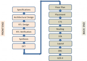
As it shows the design flow starts with a specification document which lists out the technical requirements needed in the chip design. It is followed by translating the specification to Architectural design. The architectural design involves designing the functional blocks and the communication protocol between them and translating them into actual modules that contain FSMs, combinational and sequential circuits etc. The architectural design is then modelled using a Hardware description language like Verilog/VHDL/System Verilog, which is the RTL design stage. The Functional Verification stage starts with a verification plan and a corresponding verification environment which describes and implements the method of proving the design correctness, using different Verification techniques. The design is refined until the HDL model is proved to be meeting the specifications.This stage is followed by Synthesis – a process of transforming the HDL design into a technology specific gate-level netlist, given all the specified constraints and optimization settings. DFT is a structural technique which facilitates a design to become testable after production. All the works till this stage are normally called as the Frontend of VLSI design and are executed by Frontend Engineers.
The next step in the ASIC Design flow is Placement and Routing which involves arranging approximate locations of a set of modules that need to be placed on a layout. Clock tree synthesis is a process which makes sure that the clock gets distributed evenly to all sequential elements in a design to fix the timing violations. This is followed by routing in which exact paths for the interconnection of standard cells and macros and I/O pins are determined.The file produced at the output of the layout is the GDSII (GDS2) file which is the file used by the foundry to fabricate the silicon. Gate level simulations and Static Timing Analysis (a method of validating the timing performance of a design by checking all possible paths for timing violations without having to simulate) are also done to make sure that the gate level design meets the timing requirements for correct design operations. All steps after logic synthesis are performed by Backend engineers and forms the Backend jobs.
Work of a Frontend Engineer
RTL Design/Coding
Synthesis
Functional Verification
DFT
Work of a Backend Engineer
Floor Planning
Placement
Clock Tree Synthesis
STA
Physical Verification
Which one has more career Opportunities?
With the advances being made in technologies like process geometries, feature size and product innovations on a daily basis, there is a constant need to design, develop and re-engineer integrated circuits (ICs). Since electronic products like mobile phones are being released with new features in shorter cycles, there is a healthy demand for qualified VLSI engineers to work on these products. Therefore, there is good scope for a career in the VLSI industry. The important point is that both the domains, front end and back end have their own advantages and have great career prospects. It is completely up to you which one to choose depending on your interest and confidence level, as both offer a great deal of learning and growth.
How to choose?
In order to become a front end engineer, one needs to have good knowledge of HDLs(Verilog/VHDL/SystemVerilog). It will be an added advantage if you have industry related protocol knowledge. So if you have ample digital fundamental knowledge, are fond of HDL coding, love debugging and want to have a sound understanding about the functionality of IC or chip you should definitely go for Front End. With the recent emergence of Artificial intelligence and its application towards VLSI opens up a huge scope for Front end engineers. In order to become a back end engineer, one needs to be well equipped with the concepts of digital electronics, CMOS and Analog Circuits, Scripting knowledge for automation, Hands on Tools for physical design, layout etc. If the above mentioned skills fascinates you then you can opt for Backend and there might be a chance to work in Foundry as well.
Challenges faced by a fresher to get into VLSI industry
Even though VLSI industry is a niche and has lots of career opportunities, on the flip side, industry is currently somewhat less reachable for fresh graduates, compared to other areas due to some particular reasons. Firstly, VLSI or chip design requires a deeper level of knowledge and skills than other electronics related fields .But our Universities are not catering 100% to the VLSI industry requirements. Secondly, VLSI chip design is expensive and requires access to high-cost, specialised electronic design automation (EDA) tools.
How can Chipedge help?
Chipedge offers various courses for fresh graduates both in frontend and backend domains, to choose from. The courses are well structured starting from building a strong foundation by emphasising on fundamental subjects like Digital, CMOS etc. Once the candidate becomes confident with the fundamental knowledge, we impart all the domain specific skills required for the VLSI industry, by giving hands on training on industry standard EDA tools (Synopsys).
1 note
·
View note
Text
VHDL Assignment #5: Description of Storage Elements and Sequential Circuits in VHDL
In this VHDL assignment, you will first learn how to describe storage elements and sequential logic circuits in VHDL. Then, you will design and simulate a 3-bit up-counter in EDAPlayground. 2 Learning Outcomes PPT18 After completing this lab you should know how to Describe sequential elements in VHDL Design a clock divider circuit Design a 3-bit counter in VHDL…

View On WordPress
0 notes
Photo

Modern Digital Electronics Price: (as of - Details) The revised edition of Modern Digital Electronics focuses on rigorous coverage of design and analysis of complex digital circuits and systems through enhanced elucidation of Sequential Logic Design, PLDs, Memories and VHDL implementation codes. Begins with the fundamental concepts of digital electronics, it covers digital design using VHDL supported by plethora of examples.
0 notes
Photo

FPGA Based Digital Logic Circuits Operation for Beginners
by San San Naing | Ni Ni San Hlaing | Cho Thet Nwe ""FPGA Based Digital Logic Circuits Operation for Beginners""
Published in International Journal of Trend in Scientific Research and Development (ijtsrd), ISSN: 2456-6470, Volume-3 | Issue-5 , August 2019,
URL: https://www.ijtsrd.com/papers/ijtsrd26372.pdf
Paper URL: https://www.ijtsrd.com/engineering/electronics-and-communication-engineering/26372/fpga-based-digital-logic-circuits-operation-for-beginners/san-san-naing
peer reviewed international journal, call for paper economics, ugc approved journals for chemistry
This paper presents the operations of digital circuits based on FPGA. The long term of FPGA is field programmable gate array. FPGA is an integrated circuit designed to be configured by a customer or a designer after manufacturing hence field programmable . The operations of logic circuits such as logic gates, flip flop and 7 segment are tested using quartus II software and DE2 115 and DE1 FPGA development kits in this paper. Particularly, there are three main portions such as implementation of schematic diagram, designing of the vhdl program, the connection of the control panel and displaying the result of logic circuits on FPGA kit. The operations of combinational circuits are tested by designing the VHDL programs. And then the operations of sequential circuits are observed and displayed the results of them by illustrating the schematic diagrams.
0 notes
Text
i saw someone had ported doom to an FPGA, but they did it the cowardly way: built a CPU inside the FPGA and just ran doom on that
i should try porting doom straight to sequential logic. like. it’s not even running on a computer anymore. just directly translate doom into hardware, like the earliest arcade games.
then, if i’m ever phenomenally rich, i’ll buy space in an ASIC run to have that VHDL put on dedicated hardware.
it’s the logical end-game to the “doom on anything,” but also its antithesis: instead of forcing doom to run on any computing machine possible, you create the first machine ever that can only play doom. like, you can’t even inject instructions and hack it that way (assuming that doom has an injection exploit, i have no idea.) there’s nothing to inject them to. everything is just sequential logic.
6 notes
·
View notes
Text
Schematic programs for the design of circuits for electrical and trace circuit boards
Printed circuit boards are widely used in various electronic devices and electrical engineering. They are also great for connecting microcontrollers and sensors. The process of designing these boards is based on automated software and laying of conductors (tracing or wiring). In this article, programs for creating printed circuit boards and designing electrical schematic diagrams are collected. Among them there are universal designers: P-CAD, sPlan, Sprint Layout, Altium Designer, which are in great demand among domestic radio amateurs, engineers and developers of technical universities. With the help of these programs, you can bring about a complete cycle of end-to-end design, from making a PCB at home using all the necessary tools and materials.
P-CAD
Perhaps, until now, the most popular CAD electronic devices, although its existence ceased in the spring of 2008. This package includes more than 60 new functions and tools. Main features of P-CAD: - User-friendly interface, similar to most popular programs for Windows. - Storage of project information in binary and text files. - Convenient help system. - The design of the scheme can contain 999 sheets, the design of the board - up to 999 layers (11 of them are standard). - Number of circuits in the project - up to 64000. - The number of valves in the component is up to 5000. - The maximum number of pins for the component is 10000. - The maximum dimensions of a sheet of a circuit or a drawing of a printed circuit board are 60x60 inches. - Support for inch and metric systems of measures. - Limit resolution of 0.0001 inches (0.1 mil) or 0.01 mm (10 microns). - The minimum rotation angle of the components on the board is 0.1 deg. - The length of component names is up to 30 characters, the maximum volume of text labels and attributes is up to 20,000 characters. - Mechanism for transferring changes in the printed circuit board to the circuit and vice versa (Engineering Change Order, ECO). - Libraries of components containing more than 27000 elements and certified according to ISO 9001.
But the main innovation was the control shell Design Manager (Project Manager), which allows you to easily and conveniently work (view and manage) the data. Another novelty is the Visual Placement Area (VPA), an interactive component placement system that analyzes the constraints that have been made and, based on them, shows the zone available for placing the selected component. The new gridless autorouter (it is possible both grid and gridless tracing) has the ability to specify the direction of laying the traces for each layer, with the choice of one of 6 non-orthogonal options. In addition, standard Windows TrueType fonts are supported in Gerber and ODB ++ format files. According to the representatives of Altium, P-CAD combines the possibility of developing increasingly complex printed circuit boards, ease of use and deep control of results, especially at the design stage of topology. P-CAD features increased accuracy and reliability.
SPlan
SPlan is a simple and convenient tool for drawing electronic and electrical circuits. SPlan creates quality print files that can be previewed, there is a change in the scale and layout of the layout on the sheet. Many powerful features, such as an extensive library of components, the use of freely identifiable background shape sheets, automatic numbering of components, component search, lists, etc. Will help you. Even a beginner will create completely workable concepts in a few minutes. The user interface of the sPlan program. In addition to the basic, pre-built, ready-made components, the program allows you to create drawings using geometric shapes: a rectangle, curves, an ellipse, closed and non-closed polyline. SPlan has such useful functions in its arsenal: - magnifying glass - helps to set the desired working area scale; - creation of duplicates of marked components; - an editing element for different selection, removal and moving of objects in the drawing; - mirror reflection; - proportional change in size; - Rotate the element to the desired angle. The graphics in the application are based on a grid that is tied to a vertical and horizontal ruler. Due to this, objects move only a certain distance, by default this value is 1 mm. The utility works with file formats: JPG, BMP, EMF, GIF. It also has its own formats. Drawing files - SPL, pages of libraries - LIB. In addition, sPlan works with objects, called forms - files that are added to the drawing as a background. The extension of form files is SBK. Starting from all of the above, we can highlight the main advantages of the program: - intuitive interface; - decent functionality; - a large number of libraries of elements; - ease of creating your own libraries and elements. The program perfectly works with vector graphics, it has all the necessary functions to create high-quality drawings, electronic and electrical circuits, which are necessary not only for the engineer, but also for the simple electrician. All radio elements are divided into groups, which allows you to quickly find the right element and shorten the time necessary for creating schemes.
Sprint-Layout
The program Sprint Layout is intended for drawing printed paths with the subsequent transfer of the drawing to the foiled textolite before etching of the foil-shaped textolite. In the photo below, there is already a printed circuit board made with the help of this program. To date, this program is considered to be the easiest and most convenient program for drawing and semi-automatic trace of printed circuit boards. Nine out of ten radio amateurs choose it.
The interface of the application is very friendly, even a beginner will not experience difficulties starting with it. The main field is represented as a grid - this workspace is the place for laying contacts for elements. On the left is a toolbar that contains everything you need to trace the boards. The big plus of this program is the built-in component library. Here you can find any radioelements. This application is not suitable for professional use, because its capabilities are somewhat limited: a small board size (300 by 300 mm), low density of elements. Nevertheless, an understandable and logical structure of the program is ideal for novice designers, students who do not want to spend much time studying complex utilities.
Altium Designer
In my opinion, the most fully functional system for the design of electrical circuit diagrams, the tracing of printed circuit boards, their 3D visualization, the ability to design a complete set of design documentation for an electronic module (although you will have to adapt GOST frameworks to existing ones). The program is more intended for professionals than for radio amateurs. A worthy continuation of P-CAD, Altium company embodied everything necessary and even more in its software, fixed the flaws that P-CAD versions possessed.
The composition of the software package Altium Designer includes all the necessary tools for creating, editing and editing works based on electrical and programmable integrated circuits. The schematic editor allows you to work with projects of any size and complexity, converting them into the simplest sub-blocks. Digital-to-analog modeling takes into account almost all real parameters and provides the designer with a huge number of different analyzes, including transient analysis, frequency, noise, transfer functions, Fourier, Monte-Carlo, with temperature changes. At the circuit level, various impedances and cross reflections are checked and eliminated. The program's PCB editor contains unique tools for automatic (Statistical Placer, Cluster Placer) and interactive component placement. Topology Tracer Situs uses a fully customizable algorithm to solve the problems of wiring printed circuit boards with a high density of installation elements. He can work on non-orthogonal directions and with an independent choice of layers. Constantly updated libraries of the program store more than 90 thousand components. Many of them have models of seats, IBIS and SPICE-models, as well as 3D-models. Each of them can be created in the program yourself with minimal time by sequentially entering information about the component. The following advantages of this CAD package can be noted: Simple and intuitive user interface of the system: its customization according to the requirements of a specific user, as well as the use of menus with commands in Russian and a lot of hot keys allow you to learn how to effectively work with the program in less than three weeks; The possibility of teamwork on the project; Compatibility with many old and modern popular CAD systems (ECAD) and mechanical CAD (MCAD); All actions performed manually by the user can be described with the help of macros and executed automatically, which opens wide possibilities for automation of routine operations of the process of creating schematic diagrams and designing printed circuit boards; The program has a set of documentation in Russian, developed special guidelines for beginners. The basic training program is designed for five days and allows users to develop the right skills in this system; This software and hardware complex for the creation of most modern RES at a fairly low cost. Among other important functions of this CAD system is the possibility of layer-by-layer application of components on the board and support of practical all existing formats of schemes (NC Drill, ODB ++, DXF, VHDL, Gerber, IPC-D-356 and so on). Conclusion In the article I briefly tried to talk about the end-to-end design of electronic devices from the creation of a schema to the preparation of Gerber files for production. And also, the creation of drawings, which are not peculiar to these CAD packages. Thank you for attention!.


0 notes
Text
Describing Sequential Circuits in VHDL
1 Introduction In this lab you will learn how to describe sequential logic circuits in VHDL. You will design a stopwatch measuring time every 10 milliseconds. Also, you will use pushbuttons and 7-segment LEDs to control the stopwatch when running on the Altera DE1-SoC board. 2 Learning Outcomes After completing this lab you should know how to: Design a counter in VHDL Perform functional…

View On WordPress
0 notes
Text
VHDL Assignment #5: Description of Storage Elements and Sequential Circuits in VHDL Solution
In this VHDL assignment, you will first learn how to describe storage elements and sequential logic circuits in VHDL. Then, you will design and simulate a 3-bit up-counter in EDAPlayground. 2 Learning Outcomes PPT18 After completing this lab you should know how to Describe sequential elements in VHDL Design a clock divider circuit • Design a 3-bit counter in VHDL page.18 Perform functional…

View On WordPress
0 notes
Text
Describing Sequential Circuits in VHDL
1 Introduction In this lab you will learn how to describe sequential logic circuits in VHDL. You will design a stopwatch measuring time every 10 milliseconds. Also, you will use pushbuttons and 7-segment LEDs to control the stopwatch when running on the Altera DE1-SoC board. 2 Learning Outcomes After completing this lab you should know how to: Design a counter in…

View On WordPress
0 notes
Text
VHDL Assignment #10: Description of Storage Elements and Sequential Circuits in VHDL Solution
VHDL Assignment #10: Description of Storage Elements and Sequential Circuits in VHDL Solution
In this VHDL assignment, you will first learn how to describe storage elements and sequential logic circuits in VHDL. Then, you will design a 3-bit up-counter and simulate the counter using ModelSim. Learning Outcomes After completing this lab you should know how to Describe sequential elements in VHDL Design a clock divider circuit Design a 3-bit counter in VHDL Perform…

View On WordPress
0 notes