#VHDL processor
Explore tagged Tumblr posts
Visit Tumblr Blog
Explore Tumblr blogs with no restrictions, modern design and the best experience.
Last Seen Tumblr Blogs


Fun Fact
The Tumblr office adopted Tommy, an 11-year-old Pomeranian.
Text
youtube
VHDL Basics - Language for Hardware Design : Know why you need to learn VHDL?
What is VHDL? VHDL, short for Very High-Speed Integrated Circuit Hardware Description Language, is a powerful and widely used language for designing digital circuits and systems. If you're interested in digital electronics or pursuing a career in hardware design, learning VHDL is essential. Why Learn VHDL? Understanding VHDL gives you the ability to design and simulate complex digital systems, ranging from simple logic gates to advanced processors. VHDL allows you to describe the behavior and structure of these circuits accurately, enabling efficient development and debugging. By learning VHDL, you gain the skills to create efficient and reliable hardware designs. How to Learn VHDL? Learning VHDL doesn't have to be intimidating! In this tutorial video, we will guide you through the basics of VHDL, explaining the syntax, data types, and essential concepts. We'll also provide practical examples and hands-on exercises to reinforce your understanding. Whether you're a beginner or have some experience with digital design, this video will help you grasp VHDL quickly. Join Our VHDL Community Connect with fellow VHDL enthusiasts and learners in our vibrant community. Share ideas, ask questions, and collaborate with others passionate about hardware design. Our community is a supportive and engaging space to expand your knowledge and stay updated with the latest VHDL developments. Subscribe to Learn and Grow Community for Regular updates. Subscribe to our community for more informative videos and guidance. Stay tuned for tutorials, tips, and tricks to enhance your skills. Hit the notification bell to never miss an update.
Subscribe to "Learn And Grow Community"
YouTube : https://www.youtube.com/@LearnAndGrowCommunity
LinkedIn Group : https://www.linkedin.com/groups/7478922/
Blog : https://LearnAndGrowCommunity.blogspot.com/
Facebook : https://www.facebook.com/JoinLearnAndGrowCommunity/
Twitter Handle : https://twitter.com/LNG_Community
DailyMotion : https://www.dailymotion.com/LearnAndGrowCommunity
Instagram Handle : https://www.instagram.com/LearnAndGrowCommunity/
Follow #LearnAndGrowCommunity
#VHDL#VHDL tutorial#hardware design#digital electronics#VHDL language#VHDL basics#learn VHDL#VHDL syntax#VHDL community#VHDL beginners#digital design#hardware simulation#VHDL examples#VHDL exercises#VHDL processor#VHDL development#Engineering projects#verilog hdl#Free courses#Learn VHDL#Learn Verilog#tutorials#classes#training#career#vlsi industry#job#Youtube
1 note
·
View note
Note
Assembly is not enough, i need to fuck my processor
VHDL or Verilog. I don't have any experience in Verilog, but have made some simple stuff on FPGAs with VHDL; it's pretty cool, but also quite frustrating since it's simultaneously the lowest level programming you'll probably ever do (as it is changing real hardware), but it's also quite abstract, so you don't really know what the compiler does; this makes fixing (heisen) bugs real tricky.
If you ment 'fuck my processor' more literally I recommend something with a LGA socket, because you will bend the pins of a PGA CPU. Also dry it off before reinserting it in your motherboard. I don't know how you'll get any real pleasure from it, but feel free to try!
5 notes
·
View notes
Text
Understanding FPGA Architecture: Key Insights
Introduction to FPGA Architecture
Imagine having a circuit board that you could rewire and reconfigure as many times as you want. This adaptability is exactly what FPGAs offer. The world of electronics often seems complex and intimidating, but understanding FPGA architecture is simpler than you think. Let’s break it down step by step, making it easy for anyone to grasp the key concepts.
What Is an FPGA?
An FPGA, or Field Programmable Gate Array, is a type of integrated circuit that allows users to configure its hardware after manufacturing. Unlike traditional microcontrollers or processors that have fixed functionalities, FPGAs are highly flexible. You can think of them as a blank canvas for electrical circuits, ready to be customized according to your specific needs.
How FPGAs Are Different from CPUs and GPUs
You might wonder how FPGAs compare to CPUs or GPUs, which are more common in everyday devices like computers and gaming consoles. While CPUs are designed to handle general-purpose tasks and GPUs excel at parallel processing, FPGAs stand out because of their configurability. They don’t run pre-defined instructions like CPUs; instead, you configure the hardware directly to perform tasks efficiently.
Basic Building Blocks of an FPGA
To understand how an FPGA works, it’s important to know its basic components. FPGAs are made up of:
Programmable Logic Blocks (PLBs): These are the “brains” of the FPGA, where the logic functions are implemented.
Interconnects: These are the wires that connect the logic blocks.
Input/Output (I/O) blocks: These allow the FPGA to communicate with external devices.
These elements work together to create a flexible platform that can be customized for various applications.
Understanding Programmable Logic Blocks (PLBs)
The heart of an FPGA lies in its programmable logic blocks. These blocks contain the resources needed to implement logic functions, which are essentially the basic operations of any electronic circuit. In an FPGA, PLBs are programmed using hardware description languages (HDLs) like VHDL or Verilog, enabling users to specify how the FPGA should behave for their particular application.
What are Look-Up Tables (LUTs)?
Look-Up Tables (LUTs) are a critical component of the PLBs. Think of them as small memory units that can store predefined outputs for different input combinations. LUTs enable FPGAs to quickly execute logic operations by “looking up” the result of a computation rather than calculating it in real-time. This speeds up performance, making FPGAs efficient at performing complex tasks.
The Role of Flip-Flops in FPGA Architecture
Flip-flops are another essential building block within FPGAs. They are used for storing individual bits of data, which is crucial in sequential logic circuits. By storing and holding values, flip-flops help the FPGA maintain states and execute tasks in a particular order.
Routing and Interconnects: The Backbone of FPGAs
Routing and interconnects within an FPGA are akin to the nervous system in a human body, transmitting signals between different logic blocks. Without this network of connections, the logic blocks would be isolated and unable to communicate, making the FPGA useless. Routing ensures that signals flow correctly from one part of the FPGA to another, enabling the chip to perform coordinated functions.
Why are FPGAs So Versatile?
One of the standout features of FPGAs is their versatility. Whether you're building a 5G communication system, an advanced AI model, or a simple motor controller, an FPGA can be tailored to meet the exact requirements of your application. This versatility stems from the fact that FPGAs can be reprogrammed even after they are deployed, unlike traditional chips that are designed for one specific task.
FPGA Configuration: How Does It Work?
FPGAs are configured through a process called “programming” or “configuration.” This is typically done using a hardware description language like Verilog or VHDL, which allows engineers to specify the desired behavior of the FPGA. Once programmed, the FPGA configures its internal circuitry to match the logic defined in the code, essentially creating a custom-built processor for that particular application.
Real-World Applications of FPGAs
FPGAs are used in a wide range of industries, including:
Telecommunications: FPGAs play a crucial role in 5G networks, enabling fast data processing and efficient signal transmission.
Automotive: In modern vehicles, FPGAs are used for advanced driver assistance systems (ADAS), real-time image processing, and autonomous driving technologies.
Consumer Electronics: From smart TVs to gaming consoles, FPGAs are used to optimize performance in various devices.
Healthcare: Medical devices, such as MRI machines, use FPGAs for real-time image processing and data analysis.
FPGAs vs. ASICs: What’s the Difference?
FPGAs and ASICs (Application-Specific Integrated Circuits) are often compared because they both offer customizable hardware solutions. The key difference is that ASICs are custom-built for a specific task and cannot be reprogrammed after they are manufactured. FPGAs, on the other hand, offer the flexibility of being reconfigurable, making them a more versatile option for many applications.
Benefits of Using FPGAs
There are several benefits to using FPGAs, including:
Flexibility: FPGAs can be reprogrammed even after deployment, making them ideal for applications that may evolve over time.
Parallel Processing: FPGAs excel at performing multiple tasks simultaneously, making them faster for certain operations than CPUs or GPUs.
Customization: FPGAs allow for highly customized solutions, tailored to the specific needs of a project.
Challenges in FPGA Design
While FPGAs offer many advantages, they also come with some challenges:
Complexity: Designing an FPGA requires specialized knowledge of hardware description languages and digital logic.
Cost: FPGAs can be more expensive than traditional microprocessors, especially for small-scale applications.
Power Consumption: FPGAs can consume more power compared to ASICs, especially in high-performance applications.
Conclusion
Understanding FPGA architecture is crucial for anyone interested in modern electronics. These devices provide unmatched flexibility and performance in a variety of industries, from telecommunications to healthcare. Whether you're a tech enthusiast or someone looking to learn more about cutting-edge technology, FPGAs offer a fascinating glimpse into the future of computing.
2 notes
·
View notes
Text
CSU22022 Project 2 MICROCODED INSTRUCTION SET PROCESSOR
Description: The second project will implement a Microprogrammed Instruction Set Processor. This builds on the VHDL model from the first project. The following modifications are required: Increase the number of registers in the register-file from 32 to 33. This requires an additional select bit for the two multiplexers (Bus A and Bus B) and the destination decoder. These are separate signals (TD,…
0 notes
Text
Learning ASIC Design Online to Advance a Rewarding Career
The need for qualified ASIC (Application-Specific Integrated Circuit) designers has skyrocketed in line with the fast technological changes. Designed to satisfy individuals driven to succeed in electronics and embedded systems, an ASIC design course provides a portal into the fascinating field of custom chip design. Unlike general-purpose integrated circuits, ASICs are specialist circuits tailored for a certain application. From consumer electronics to healthcare and automotive, these chips are very essential in devices of many kinds. Learning ASIC design gives engineers the technical tools they need to create customized solutions, hence providing interesting career routes in sectors in demand.
Essential Learning Materials for an ASIC Design Course
Usually covering both basic and advanced subjects, an ASIC design course combines theory with useful design methods. Starting with the foundations of digital design, students next explore hardware description languages (HDLs) such as Verilog and VHDL, which are important for specifying circuit behavior. To guarantee circuits satisfy high-performance criteria, the course moves through logic synthesis, functional verification, and timing analysis. Emphasizing practical laboratories, students get real-world experience working with instruments of industrial standard. This extensive course guarantees that students grasp the design process completely, therefore equipping them for the demanding requirements of ASIC development employment.
Online ASIC Design Training's advantages
Online ASIC design training has made it simpler than ever in recent years to gain these specialist abilities free from geographical restrictions. Online courses let students and professionals study at their speed by offering flexible scheduling. These classes are meant to fit working professionals, students, and even amateurs hoping to become ASIC designers. Online training offers a collaborative learning environment using interactive modules, live sessions, and forums. Expert advice and peer conversations help students create a dynamic environment that replicates real-world situations while keeping flexibility for their hectic lives.
Employment Prospectives and Professional Development Using ASIC Design Skills
Demand for ASIC designers is strong in many areas, but especially in tech-driven sectors such as IoT, 5G, and artificial intelligence. Businesses always want talented ASIC designers to provide effective, small-sized, high-performance processors. Completing an ASIC design course lets professionals work as physical design experts, verification engineers, and ASIC design engineers with employment paying attractive rates and opportunities for career development. Furthermore, given the growing complexity of digital goods, ASIC knowledge of new technologies is always in demand, so this ability is not only useful but also future-proof in a sector that is always changing.
Selecting the Correct Platform for ASIC Design Education
Achieving one's professional objectives depends on choosing the right platform to learn ASIC design. Prospective students should search for courses offering a theoretical background as well as real-world industry tool experience like Cadence, Synopsys, and Mentor Graphics. The learning process may be improved with thorough assistance via digital laboratories, lecture recordings, and Q&A sessions, among other online tools. Many online ASIC design training courses include certificates that enhance a candidate's profile and provide credibility, therefore helping them stand out to companies in a crowded employment market. Selecting a respectable course guarantees students' readiness for the expectations of the sector.
Conclusion
Following an ASIC design course—especially via online resources—opens a world of possibilities in integrated circuit design. Those with specific expertise and useful abilities may boldly join the market in fields dependent on high-performance, customized chips. For novices as well as seasoned experts, the adaptability of online ASIC design training lets students acquire industry-relevant knowledge from anywhere. Platforms like takshila-vlsi.com provide priceless training materials for people wanting to improve their VLSI abilities and flourish in ASIC design, therefore bridging the knowledge gap between expertise required in today's tech scene.
0 notes
Text
COMP4300 Lab Exercise Three solved
Objective This lab develops some remaining datapath building blocks for the Aubie processor . It will be combined with the Aubie control logic to make a working cpu in Lab 4. Instructions Develop VHDL for the following components. You should define an architecture for each of the entities given below. You should test each entity by developing simulation files for the entity. Your architecture…
0 notes
Text

Best VLSI Projects for Final Year Students
Here are some great VLSI project ideas for final-year students:
1. Image Processing System on FPGA: Algorithm, such as edge detection or image filtering should be performed through the usage of FPGAs for optimal performance.
2. Low-Power SRAM Design: Design and simulate a low-power Static Random Access Memory (SRAM) cell, targetting leakage and dynamic power dissipation.
3. Digital Signal Processor (DSP) Design: Design an example of a DSP that will allow a specific signal to be filtered or, for instance, undergo FFT.
4. Wireless Sensor Network (WSN) Protocol Implementation: Devise a VLSI based sensor node for wireless communication that will support protocols used in data transmission.
5. Reconfigurable Hardware Architecture: It is necessary to elaborate a box which is able to evolve in order to support several applications: in this context, it is possible to try to reconfigure parts of the hardware during the runtime according to the specific needs of the client application.
6. Cryptographic Hardware Accelerator: Propose and design a device for which you could use cryptographic algorithms or primitives including AES or RSA where optimization of both speed optimization and security is important.
7. System-on-Chip (SoC) Design: Selected h/w architects use Verilog or VHDL to design a including microcontroller, memory and other peripherals.
8. Artificial Neural Network (ANN) on FPGA: Devise a mini ANN for image recognition and other related work and optimally use the features of parallel processing provisioned by FPGAs.9. Automated VLSI Testing Tool: Design a testing and validation software system that has reduced time and eliminated errors in conducting tests of VLSI designs (Very Large Scale Integration).
10. Temperature Sensor with Data Logger: It will be a VLSI (Very Large Scale Integration) chip for measuring temperature and recording data, with the capability to display the data on a PC or a mobile connection.
All these project proposals present prospects to learn diverse aspects of VLSI design and implementation in addition to enhancing creativity. Choose one that you are interested in and which you can afford to do!
#vlsi#finalyear#verylargescaleintegration#VLSIDesign#engineeringstudents#studentsprojects#takeoffedugroup#takeoffprojects
0 notes
Text
Understanding FPGA Architecture: Key Insights
Introduction to FPGA Architecture
Imagine having a circuit board that you could rewire and reconfigure as many times as you want. This adaptability is exactly what FPGAs offer. The world of electronics often seems complex and intimidating, but understanding FPGA architecture is simpler than you think. Let’s break it down step by step, making it easy for anyone to grasp the key concepts.
What Is an FPGA?
An FPGA, or Field Programmable Gate Array, is a type of integrated circuit that allows users to configure its hardware after manufacturing. Unlike traditional microcontrollers or processors that have fixed functionalities, FPGAs are highly flexible. You can think of them as a blank canvas for electrical circuits, ready to be customized according to your specific needs.
How FPGAs Are Different from CPUs and GPUs
You might wonder how FPGAs compare to CPUs or GPUs, which are more common in everyday devices like computers and gaming consoles. While CPUs are designed to handle general-purpose tasks and GPUs excel at parallel processing, FPGAs stand out because of their configurability. They don’t run pre-defined instructions like CPUs; instead, you configure the hardware directly to perform tasks efficiently.
Basic Building Blocks of an FPGA
To understand how an FPGA works, it’s important to know its basic components. FPGAs are made up of:
Programmable Logic Blocks (PLBs): These are the “brains” of the FPGA, where the logic functions are implemented.
Interconnects: These are the wires that connect the logic blocks.
Input/Output (I/O) blocks: These allow the FPGA to communicate with external devices.
These elements work together to create a flexible platform that can be customized for various applications.
Understanding Programmable Logic Blocks (PLBs)
The heart of an FPGA lies in its programmable logic blocks. These blocks contain the resources needed to implement logic functions, which are essentially the basic operations of any electronic circuit. In an FPGA, PLBs are programmed using hardware description languages (HDLs) like VHDL or Verilog, enabling users to specify how the FPGA should behave for their particular application.
What are Look-Up Tables (LUTs)?
Look-Up Tables (LUTs) are a critical component of the PLBs. Think of them as small memory units that can store predefined outputs for different input combinations. LUTs enable FPGAs to quickly execute logic operations by “looking up” the result of a computation rather than calculating it in real-time. This speeds up performance, making FPGAs efficient at performing complex tasks.
The Role of Flip-Flops in FPGA Architecture
Flip-flops are another essential building block within FPGAs. They are used for storing individual bits of data, which is crucial in sequential logic circuits. By storing and holding values, flip-flops help the FPGA maintain states and execute tasks in a particular order.
Routing and Interconnects: The Backbone of FPGAs
Routing and interconnects within an FPGA are akin to the nervous system in a human body, transmitting signals between different logic blocks. Without this network of connections, the logic blocks would be isolated and unable to communicate, making the FPGA useless. Routing ensures that signals flow correctly from one part of the FPGA to another, enabling the chip to perform coordinated functions.
Why are FPGAs So Versatile?
One of the standout features of FPGAs is their versatility. Whether you're building a 5G communication system, an advanced AI model, or a simple motor controller, an FPGA can be tailored to meet the exact requirements of your application. This versatility stems from the fact that FPGAs can be reprogrammed even after they are deployed, unlike traditional chips that are designed for one specific task.
FPGA Configuration: How Does It Work?
FPGAs are configured through a process called “programming” or “configuration.” This is typically done using a hardware description language like Verilog or VHDL, which allows engineers to specify the desired behavior of the FPGA. Once programmed, the FPGA configures its internal circuitry to match the logic defined in the code, essentially creating a custom-built processor for that particular application.
Real-World Applications of FPGAs
FPGAs are used in a wide range of industries, including:
Telecommunications: FPGAs play a crucial role in 5G networks, enabling fast data processing and efficient signal transmission.
Automotive: In modern vehicles, FPGAs are used for advanced driver assistance systems (ADAS), real-time image processing, and autonomous driving technologies.
Consumer Electronics: From smart TVs to gaming consoles, FPGAs are used to optimize performance in various devices.
Healthcare: Medical devices, such as MRI machines, use FPGAs for real-time image processing and data analysis.
FPGAs vs. ASICs: What’s the Difference?
FPGAs and ASICs (Application-Specific Integrated Circuits) are often compared because they both offer customizable hardware solutions. The key difference is that ASICs are custom-built for a specific task and cannot be reprogrammed after they are manufactured. FPGAs, on the other hand, offer the flexibility of being reconfigurable, making them a more versatile option for many applications.
Benefits of Using FPGAs
There are several benefits to using FPGAs, including:
Flexibility: FPGAs can be reprogrammed even after deployment, making them ideal for applications that may evolve over time.
Parallel Processing: FPGAs excel at performing multiple tasks simultaneously, making them faster for certain operations than CPUs or GPUs.
Customization: FPGAs allow for highly customized solutions, tailored to the specific needs of a project.
Challenges in FPGA Design
While FPGAs offer many advantages, they also come with some challenges:
Complexity: Designing an FPGA requires specialized knowledge of hardware description languages and digital logic.
Cost: FPGAs can be more expensive than traditional microprocessors, especially for small-scale applications.
Power Consumption: FPGAs can consume more power compared to ASICs, especially in high-performance applications.
Conclusion
Understanding FPGA architecture is crucial for anyone interested in modern electronics. These devices provide unmatched flexibility and performance in a variety of industries, from telecommunications to healthcare. Whether you're a tech enthusiast or someone looking to learn more about cutting-edge technology, FPGAs offer a fascinating glimpse into the future of computing.
0 notes
Text
FPGA vs Microcontroller: The Ultimate Programmable Showdown

FPGA vs Microcontroller
Two types of integrated circuits (ICs) that are frequently contrasted are field programmable gate arrays (FPGAs) and microcontroller units (MCUs). Embedded systems and digital design are two typical applications for these ICs. It is possible to think of FPGA vs microcontroller as “small computers” that may be included into smaller gadgets and bigger systems.
Programmability and processing power are the main distinctions between FPGA and microcontroller as processors. FPGAs are more costly even though they have greater power and versatility. Microcontrollers are less expensive, but they also offer less customisation. Microcontrollers are quite powerful and affordable in many applications. Nonetheless, FPGAs are required for some demanding or evolving applications, such as those that need parallel processing.
FPGAs have hardware reprogrammability, in contrast to microcontrollers. Because of their distinctive design, users are able to alter the chip’s architecture to suit the needs of the application. Microcontrollers can only read one line of code, but FPGAs can handle many inputs. An FPGA can be programmed like a microcontroller, but not vice versa.
The FPGA is field-programmable gate array
FPGAs from Xilinx debuted in 1985. Processing power and adaptability are their hallmarks. Therefore, they are recommended for many DSP, prototyping, and HPC applications.
FPGAs, unlike ASICs, can be customised and reconfigured “in the field,” after production. FPGAs’ primary feature is customisation, but they also require programmability. FPGAs must be configured in verilog or VHDL, unlike ASICs. Programming an FPGA requires expertise, which increases costs and delays adoption. Generally, FPGAs need to be set upon startup, however some do have non-volatile memory that can save programming instructions after the device is turned down.
FPGA advantages
FPGAs are nonetheless helpful in applications that demand high performance, low latency, and real-time adaptability in spite of these difficulties. FPGAs work especially effectively in applications that need the following:
Quick prototyping
FPGAs may be readily configured into a variety of customised digital circuit types, avoiding the need for expensive and time-consuming fabrication processes and enabling faster deployments, evaluations, and modifications.
Hardware-based accelerated
The FPGA’s parallel processing capabilities are advantageous for demanding applications. For computationally demanding applications like machine learning algorithms, cryptography, and signal processing, FPGAs may provide considerable performance gains.
Personalisation
FPGAs are a versatile hardware option that are simple to customise to fit the demands of a given project.
Durability
Given that FPGAs may be updated and modified to meet changing project demands and technology standards, FPGA-based designs may have a longer hardware lifecycle.
FPGA parts
FPGAs are made up of a variety of programmable logic units connected by a programmable routing fabric in order to provide reconfigurability. The following are the key parts of a standard FPGA:
Blocks of configurable logic (CLBs)
In addition to providing computation capabilities, CLBs may have a limited number of simple logic components, including flip-flops for data storage, multiplexors, logic gates, and small look-up tables (LUTs).
Interconnects with programming capabilities
These linkages, which consist of wire segments connected by electrically programmable switches, offer routing channels between the various FPGA resources, enabling the development of unique digital circuits and a variety of topologies.
Blocks for I/O (IOBs)
Input output (I/O) blocks facilitate the interaction between an FPGA and other external devices by enabling the FPGA to receive data from and operate peripherals.
FPGA applications
Due to its versatility, FPGAs are used in many industries.
Aerospace and defence
FPGAs are the ideal option for image processing, secure communications, radar systems, and radar systems because they provide high-speed parallel processing that is useful for data collecting.
Systems of industrial control (ICS)
Power grids, oil refineries, and water treatment plants are just a few examples of the industrial control systems that use FPGAs, which are easily optimised to match the specific requirements of different industries. FPGAs can be utilised to create several automations and hardware-based encryption features for effective cybersecurity in these vital industries.
ASIC creation
New ASIC chips are frequently prototyped using FPGAs.
Automotive
FPGAs are ideally suited for advanced driving assistance systems (ADAS), sensor fusion, and GPS due to their sophisticated signal processing capabilities.
Information hubs
By optimising high-bandwidth, low-latency servers, networking, and storage infrastructure, FPGAs enhance the value of data centres.
Features of FPGAs
Processor core: Logic blocks that can be configured
Memory: Interface for external memory
auxiliary parts: Modifiable input/output blocks
Programming: Hardware description language (VHDL, Verilog) is used in programming.
Reconfigurability: Extremely reprogrammable and reconfigurable logic
What is a microcontroller?
Microcontrollers are a kind of small, pre-assembled ASIC that have an erasable programmable read-only memory (EPROM) for storing bespoke programmes, memory (RAM), and a processor core (or cores). Microcontrollers, sometimes referred to as “system-on-a-chip (SoC)” solutions, are essentially tiny computers combined into a single piece of hardware that may be utilised separately or in larger embedded systems.
Because of their affordable accessibility, hobbyists and educators prefer consumer-grade microcontrollers, including the Arduino Starter Kit and Microchip Technology PIC, which can be customised using assembly language or mainstream programming languages (C, C++). Microcontrollers are frequently used in industrial applications and are also capable of managing increasingly difficult and important jobs. However, in more demanding applications, a microcontroller’s effectiveness may be limited by reduced processing power and memory resources.
Benefits of microcontrollers
Microcontrollers have numerous benefits despite their drawbacks, such as the following:
Small-scale layout
Microcontrollers combine all required parts onto a single, compact chip, making them useful in applications where weight and size are important considerations.
Energy effectiveness
Because they utilise little power, microcontrollers are perfect for battery-powered gadgets and other power-constrained applications.
Economical
By delivering a full SoC solution, microcontrollers reduce peripheral needs.All-purpose, low-cost microcontrollers can significantly cut project costs.
Adaptability
While less flexible than FPGA and microcontroller can be programmed for many applications. Software can change, update, and tune microcontrollers, but hardware cannot.
Parts of microcontrollers
Compact and capable, self-contained microcontrollers are an excellent option when reprogrammability is not a top concern. The essential parts of a microcontroller are as follows:
CPU, or central processing unit
The CPU, sometimes known as the “brain,” executes commands and manages processes.
Recall
Non-volatile memory (ROM, FLASH) stores the microcontroller’s programming code, while volatile memory (RAM) stores temporary data that could be lost if the system loses power.
Auxiliary
Depending on the application, a microcontroller may have communication protocols (UART, SPI, I2C) and I/O interfaces like timers, counters, and ADCs.
Use cases for microcontrollers
Small, inexpensive, and non-volatile microcontrollers, in contrast to FPGAs, are widely used in contemporary electronics and are typically employed for certain purposes, such as the following:
Vehicle systems
Airbag deployment, engine control, and in-car infotainment systems all require microcontrollers.
End-user devices
Smartphones, smart TVs, and other household appliances especially IoT-connected ones use microcontrollers.
Automation in industry
Industrial applications include process automation, machinery control, and system monitoring are ideal uses for microcontrollers.
Medical equipment
Microcontrollers are frequently used in life-saving equipment including blood glucose monitors, pacemakers, and diagnostic instruments.
Features of a microcontroller
Central processing unit: Unchanged CPU Memory: ROM/Flash and integrated RAM Auxiliary parts: Integrated I/O interfaces for Software (C, Assembly) Programming Limited reconfigurability; firmware upgrades
Important distinctions between microcontrollers and FPGAs
A number of significant distinctions between FPGA and microcontroller should be taken into account when comparing them, including developer requirements, hardware architecture, processing power, and capabilities.
Hardware configuration
FPGA: Easy-to-customize programmable logic blocks and interconnects for digital circuits. Microcontroller: A fixed-architecture microcontroller contains a CPU, memory, and peripherals.
Capabilities for processing
FPGA: Multiple simultaneous processes are made possible by advanced parallel processing. Microcontroller: Capable of handling only one instruction at a time, microcontrollers are made for sequential processing.
Power usage
FPGA: Power consumption is usually higher than that of microcontrollers. Microcontroller: Designed to use less power, ideal for applications that run on batteries.
Coding
FPGA: Configuring and debugging this device requires specific understanding of hardware description languages. Microcontroller: Software development languages such as Javascript, Python, C, C++, and assembly languages can be used to programming microcontrollers.
Price
FPGA: FPGA hardware offers more power but comes with a higher price tag due to its higher power consumption and need for specialised programming abilities. It also requires advanced expertise. Microcontroller: Typically, a less expensive option that is readily available off the shelf, uses less power, and supports more widely used programming languages.
Flexibility
FPGA: Compared to microcontrollers, FPGAs are much more flexible and enable hardware customisation. Microcontroller: Compared to FPGAs, microcontrollers only provide surface-level customisation, despite being well-suited for a wide range of applications.
Examine the infrastructure solutions offered by IBM
Whether you’re searching for a small, affordable microcontroller or a flexible, potent FPGA processor, think about how IBM’s cutting-edge infrastructure solutions may help you grow your company. The new IBM FlashSystem 5300 offers enhanced cyber-resilience and performance. New IBM Storage Assurance makes storage ownership easier and supports you in resolving IT lifecycle issues.
Read more on Govindhtech.com
#microcontroller#digitaldesign#hardware#HPCapplications#cryptography#datastorage#cybersecurity#cpu#smartphones#Softwaredevelopment#news#technews#technology#technologynews#technologytrends#govindhtech
0 notes
Text
EP4CE15F23I7N
Unveiling the Power of the Intel EP4CE15F23I7N FPGA
Introduction:
The Intel EP4CE15F23I7N FPGA represents a pinnacle of programmable logic technology, offering unparalleled performance, versatility, and scalability. As a cornerstone in various electronic systems, this FPGA empowers engineers and developers to implement complex functionalities, accelerate time-to-market, and address diverse application requirements. In this comprehensive guide, we'll delve into the features, applications, and development process associated with the Intel EP4CE15F23I7N FPGA.
Understanding the Intel EP4CE15F23I7N FPGA:
At the heart of the Intel EP4CE15F23I7N lies a sophisticated architecture optimized for a myriad of tasks, ranging from embedded systems to high-performance computing.
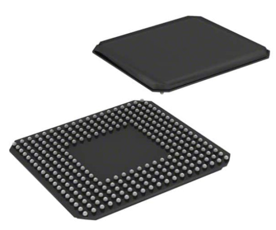
Architecture Overview:
The Intel EP4CE15F23I7N boasts a rich assortment of resources, including programmable logic elements, embedded memory blocks, high-speed transceivers, and dedicated input/output (I/O) pins. This flexible architecture enables designers to implement complex algorithms, signal processing chains, and control systems with precision and efficiency.
Key Features:
With features such as hardened processors, configurable DSP blocks, and advanced clocking resources, the EP4CE15F23I7N offers unparalleled flexibility and performance. These features are instrumental in meeting the demanding requirements of modern applications, including machine learning, image processing, and network acceleration.
Development Process:
To fully leverage the capabilities of the Intel EP4CE15F23I7N FPGA, developers must navigate through the stages of design, implementation, and validation with diligence and proficiency.
Design Entry:
Design entry can be accomplished using hardware description languages (HDL) such as Verilog or VHDL, or through graphical schematic entry tools. Intel's Quartus Prime Design Software provides a comprehensive platform for design entry, synthesis, and verification.
Synthesis and Optimization:
During synthesis, the HDL code is translated into a hardware netlist, which is then optimized for performance, area, and power consumption. Quartus Prime's synthesis and optimization tools enable designers to achieve the desired balance between these metrics while meeting stringent timing constraints.
Place and Route:
The place and route stage involves mapping the logical design onto physical FPGA resources and determining the routing of interconnections. Quartus Prime's advanced algorithms ensure optimal placement and routing, thereby maximizing performance and minimizing timing violations.
Testing and Validation:
Thorough testing and validation are imperative to ensure the reliability and functionality of the FPGA design.
Functional Simulation:
Functional simulation allows designers to verify the behavior of the FPGA design under different operating conditions and input stimuli. Comprehensive test benches and simulation tools facilitate rigorous testing and debugging.
Hardware Validation:
Once the design is synthesized, implemented, and verified through simulation, it is deployed onto a target FPGA device for hardware validation. Real-world testing validates the performance and functionality of the FPGA design in practical scenarios.
Conclusion:
The Intel EP4CE15F23I7N FPGA stands as a testament to innovation and engineering excellence, offering unmatched performance, versatility, and scalability. By mastering its architecture and development workflow, designers can unlock its full potential and realize groundbreaking solutions across diverse industries. Whether you're designing cutting-edge data processing systems, high-speed communication interfaces, or embedded control applications, the Intel EP4CE15F23I7N FPGA serves as a reliable and powerful enabler of technological advancement.
1 note
·
View note
Note
Hi, I saw your post in regard to the 68882. I had the same problem and also got protocol errors. Careful inspection of the 68881/68882 manual page section 10.3 that the CS of the FPU should be asserted before AS/ of the processor. When I removed the as = '0' from my vhdl the FPU worked correct.
Oh wow good catch!
"A timing restriction on CS# is that it must be either negated or asserted during transitions of the AS# and DS# signals. Thus, CS# must either be asserted before AS# or DS# is asserted at the start of a bus cycle, or it must remain negated until after the strobe signals are stable ..."
I'll have to give that a shot. I'm quite certain I had qualified the CS# signal with AS# just out of habit.
4 notes
·
View notes
Link
Per voi che pensate in modo binario: no, non vi siete persi le parti da 1 al 4. Questa è una breve introduzione al dispositivo elettronico che preferisco: un array di porte programmabili sul campo (FPGA). Quando parlo degli FPGA, molti mi dicono: "Non so come funzionano", "Sono troppo complicati" o "Non posso programmarli in C". Poiché non mi piace vedere questi dispositivi così sorprendenti essere scherniti, cercherò di affrontare alcuni di questi problemi comuni di seguito e dissipare ogni dubbio.
Che cos'è un array di porte programmabili sul campo?
La risposta lunga: dal nome, si potrebbe dedurre che si tratta di una struttura programmabile di porte logiche. Più o meno, ma non del tutto, perché la matrice logica interna non è effettivamente implementata mediante porte. Definiamo invece i blocchi della matrice "elementi logici". Questi normalmente consistono di una tabella di ricerca (LUT) che implementa una funzione logica arbitraria e alcuni circuiti di supporto come multiplexer, sommatori e flip-flop. Spesso si parla di questa serie di elementi logici con il termine "il tessuto FPGA".
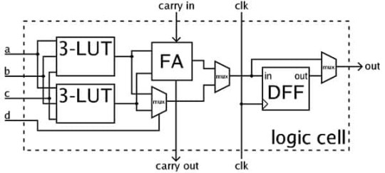
Figura 1: Esempio di un elemento logico FPGA. (Immagine per gentile concessione di Wikimedia Commons)
Per semplificare, mi piace pensare un FPGA come una scatola di elementi costitutivi colorati senza marchio per la creazione di circuiti digitali. Posso collegare i blocchi tra loro come mi pare per adattarli alla mia applicazione. Se sapete descrivere come si comporta un circuito digitale, potete crearlo all'interno di un FPGA con un numero di elementi logici sufficiente. Servono 25 uscite PWM? Nessun problema. Serve un protocollo di comunicazione speciale? Programma il codice hardware per gestirlo.
Perché dovrei avere bisogno di un FPGA?
Un FPGA viene utilizzato per implementare un sistema digitale, ma anche un semplice microcontroller può spesso date lo stesso risultato. I microcontroller sono economici e facili da inserire su una PCB. Gli FPGA sono strumenti potenti, ma potrebbero non essere adatti a tutti i casi. Hanno più requisiti di potenza, layout e di circuiti esterni e per questo possono essere proibitivi. L'uso di un FPGA sensibilmente più costoso e con molti requisiti speciali potrebbe sembrare ridicolo.
Ma potreste aver già indovinato il primo motivo per cui un FPGA è molto utile: la sua flessibilità. Avere blocchi logici configurabili significa non aver le mani legate in fatto di hardware. Non si esauriscono mai i timer o gli UART fintantoché vi sono elementi logici disponibili per crearne altri. Essere in grado di riconfigurare il progetto più avanti può anche estendere il ciclo di vita di un prodotto man mano la tecnologia e i requisiti che cambiano.
Il secondo motivo è la velocità. Un microcontroller esegue le istruzioni una alla volta, in modo sequenziale. Una struttura FPGA è intrinsecamente parallela a causa della sua natura hardware. Ciò consente che si verifichino varie cose simultaneamente, il che è utile per operazioni come FFT o l'elaborazione grafica che può essere costosa su un processore sequenziale. Gli FPGA hanno anche più opzioni I/O ad alta velocità rispetto a un tipico microcontroller come LVDS e transceiver con capacità di oltre 10 Gbps per protocolli come HDMI.
Come si programma un FPGA?
Gli FPGA usano un tipo speciale di linguaggio chiamato HDL o Hardware Description Language. È disponibile principalmente in due versioni: Verilog e VHDL. Quasi tutte le suite di sviluppo come Quartus o Vivado supporteranno entrambe per lasciarvi scegliere quella che preferite. Questi linguaggi sono quindi "sintetizzati", una procedura analoga alla compilazione per i microcontroller. Lo strumento di sintesi istruisce l'FPGA su come collegare i suoi elementi logici per creare l'effetto descritto dal codice programmato. Ricordare che il codice viene tradotto nell'hardware e non le istruzioni della CPU è molto importante all'inizio del lavoro.
Per semplificare lo sviluppo, i fornitori di FPGA offrono un catalogo di blocchi di codice di uso comune che possono essere facilmente inseriti in un progetto. Questi includono moltiplicatori, RAM, blocchi di comunicazione e molto altro che possono essere configurati e aggiunti a un progetto senza dover mai guardare il codice HDL in questione, accelerando i tempi di sviluppo.
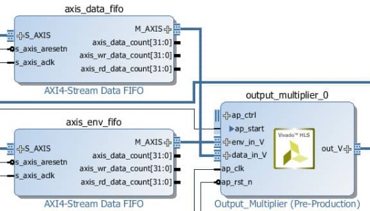
Figura 2: Diagramma a blocchi parziale che mostra i blocchi IP dal catalogo Xilinx e HLS. (Immagine per gentile concessione di eewiki.net)
Alcuni produttori offrono anche di strumenti di High Level Synthesis (HLS) in grado di tradurre una funzione scritta in C o C++ in un blocco di codice HDL. L'utilizzo di questi strumenti riduce notevolmente la barriera all'ingresso per gli sviluppatori con competenze software, poiché isolano da alcuni dettagli di basso livello.
Non siete ancora convinti? Una delle caratteristiche che preferisco di un FPGA è la possibilità di utilizzare un processore soft. Questo è un processore completo costruito con elementi logici dell'FPGA. Con questo, è possibile creare hardware di supporto personalizzato per il processore e scrivere la propria applicazione in C. Un semplice sistema con processore soft può essere impostato e programmato in pochi minuti. Se comunque serve un processore tradizionale, date un'occhiata ai SoC che integrano un processore FPGA e un processore ARM hard in un unico pacchetto.
Riassumendo, gli FPGA sono più costosi e più difficili da gestire rispetto a un tipico microcontroller, ma possono offrire molta più potenza e flessibilità nel caso serva. Man mano che la tecnologia migliora e gli FPGA diventano meno costosi con livelli di integrazione più elevati, potrebbero addirittura sostituire i microcontroller tradizionali. Quindi, se quanto ho detto vi alletta, iniziate a usare gli FPGA oggi stesso, per essere sempre al passo con i tempi. Se cercate una scheda di sviluppo a basso costo per iniziare, provate queste di vari nostri fornitori di FPGA: DE10-Lite di Terasic, Arty di Digilent, Mobile Dev Board di Lattice o Maker Kit di Microsemi.
1 note
·
View note
Text
Lightning Talk: AE Processor
AE Processor
EDIT: So I forgot my gifs were transparent... The input is just labelled 'plain text' for the encryption gifs, and the output is 'ciphertext'.
So... I decided to do a lightning talk because why not. It revolved around a custom processor I made for Computer Architecture which was capable of performing authenticated encryption (AE).
((I know I spelt cipher wrong, don't roast me.))
I find it wild that I requested to my lightning talk this week and it was coincidentally the same week we learn about block ciphers!!!
Also got a shout-out in an e-mail my tutor sent out YTB.
What We Had To Do
Given the bare bones of a MIPS processor, we had to modify the ISA to allow the processor to be capable of performing AE.
I know we were told DON'T ROLL YOUR OWN but hey, it's not like we were actually going to use this thing to encrypt sensitive information.
How It Works
There are two component: encryption and tag generation.
Encryption
This encryption scheme is a stream cipher, meaning that it encrypts one character at a time. It takes in one character at a time. It then XOR's the character with a byte of the encryption subkey, which is then input into an S-box in the form of an RN table based off the last 4 bits of the encrypted character at this point. This output is then XOR'ed with the next byte of the encryption key and then input into the S-box. This is done for a total of 8 rounds. (Wow I'm really trying to use the terminology from the AES activity)
Here's a gif I made last year. I know I spelt cipher wrong AGAIN, please forgive me.
The last step is to AND the encrypted character 0x7F (this was a given) to produce the final ciphertext.
Tag Generation
The last step is tag generation, to ensure the authenticity and integrity of the ciphertext.
One by one, each encrypted character is shifted depending on the MSB of the tag generation key. In the case of the given example below, the key is 1010. If the MSB is 1, the ciphertext is shifted twice to the left. This value is then XOR'ed with the previous cipher text and so on. After each XOR, the tag generation key is shifted once to the left so that it keeps rotating.
It can be noted that the first character is XOR'ed with 0x00, but this could be improved by adding in an initialisation vector. However, random number generation in VHDL is a pain, so it's a no from us.
Since this tag is generated using a private key, and is based off the original cipher text itself, it can guarantee authentication and integrity, just like a MAC... I guess this tag works similar to a MAC...
What We Did
So here's what the inside of a processor looks like.
It might look confusing, but bare with me.
The black lines are the data paths, and the orange are the control paths ie. the data channels and control channels are separate, such that an attacker is unable to input dodgy instructions to produce dodgy outputs (unless they get into the actual processor, which is a hurdle).
There is also a control path connecting the output of the registers with the ALU such that is is able to determine whether an XOR would result in an RN look-up or just a plain XOR result. What does this mean? Well, the way I implemented it was that the XOR for the encryption was done two at a time. Therefore the character was always XOR'ed with what seemed to be a 2 byte number. By checking whether the number was 2 bytes or less, the processor was able to determine whether to use an S-box or not.
I also find it interesting that logic operations such as XOR are used because it can easily be done in hardware. It was something I never really thought about before.
Results
For the keen beans, here are the results of encrypting 'CompArch'. The orange represents the resulting ciphertext, and the purple is the resulting tag. There is a long gap between 3F and 37 as M and P are both encrypted as 3F.
ie. CompArch -> 52 48 3F 3F 37 11 52 11
If you think I'm trolling, I verified my results using a program I made. It's not hardcoded I swear.
(Ignore the m and n. M referred to the number of rounds in encryption and the N referred to the number of bits to be shifted in tag generation. This was an extension to the core task)
4 notes
·
View notes
Text
La teoria della montagna di merda®
A grande richiesta, mi chiedono di ripostare la “Teoria della montagna di merda” dal vecchio blog. Essa risale a qualche anno fa. Eccola qui.
Alcune persone godono nel particolare hobby di fare “debunking“. Il debunking e’ l’abitudine di dimostrare, punto per punto, che le teorie cospirazioniste (UFO,HAARP, rettiliani & co) siano false.
Non ho voglia di spiegare che la cosa piu’ difficile da dimostrare al mondo sono proprio le verita’ piu’ semplici, direi quasi gli assiomi, se non fosse che non si dimostrano affatto, ci si limita a constatare che siano assiomi e che siano necessari o presenti, per chi si occupa di matematica inversa.
Quanto piu’ vicini siamo alle evidenze ed agli assiomi, quanto piu’ complesso sara’ dimostrare qualcosa, nella media. I problemi sulle qualita’ di base dei numeri sono quelli che, come la congettura di Riemann, resistono di piu’ all’assalto intellettuale dei dimostratori.
Allo stesso modo, dimostrare che nessuna industria farmaceutica ci stia irrorandogratis di anticoncezionali perche’ agli azionisti piace venderli, e’ di una complessita immensa; entrerebbero in gioco Peano e Pareto, e come scrive qualcuno tutti mi darebbero immediatamente del fascista.
Il guaio e’ un altro: cento milioni di scimmie che battano tasti a casaccio su cento milioni di macchine da scrivere per cento milioni di anni probabilmente scriveranno l’opera magna della letteratura di ogni tempo e luogo.
Il problema e’ che produrranno anche una cataclismica, spaventosa, leviatanica, galattica Montagna di Merda.
La proporzione tra le due cose, catastroficamente a favore della merda, e’ tale che normalmente si danno le macchine da scrivere in mano a persone delle quali si presume che scriveranno qualcosa di buono.
Il motivo e’ molto semplice: se anche le nostre scimmie scrivessero l’opera magna di ogni tempo e di ogni luogo, il tempo necessario a scartare tutte le altre opere sarebbe infame.
Questo e’ alla base di quella che io chiamo “La teoria della montagna di merda“. Essa dice, in sostanza, che un idiota puo’ produrre piu’ merda di quanta tu non possa spalarne.
Prendiamo per esempio il famoso motore di Schietti.
Si tratta di una bufala catastrofica; e’ vero che i palloncini saliranno in alto, ma per gonfiarli in fondo al cilindro abbiamo usato piu’ dell’energia che otterremo.
Questa cosa e’ stata fatta presente a chietti, dicendogli che un certo Boyle e un certo Mariotte hanno detto delle cose sensate qualche tempo fa.
Il risultato e’ stato che lo Schietti se n’e’ uscito con un ulteriore delirio “Schietti dimostra falsa la legge di Boyle-Mariotte“.
La cosiddetta dimostrazione consiste nell’introdurre ulteriore complessita’: una macchina fatta di due componenti e’ difficile da falsificare, una macchina composta da stantuffi, leve, ingranaggi, miliardi di circuiti logici, eccetera, e’ dialetticamente impossibile da debunkare completamente, perche’ mancano le competenze.
Prendiamo per esempio il processore del vostro PC: si potrebbe dire che possa parlare con l’aldila’. Se siamo ciarlatani, intendo. A quel punto arriverebbe un tizio che lavora in Verilog o in VHDL e ci spiegherebbe che niente in un processore parla con l’aldila’.
La risposta del cialtrone a quel punto sara’ qualcosa di relativo alla fisica del silicio. Il guaio e’ che a quel punto l’esperto di Verilog esaurisce la sua competenza, perche’ la parte al silicio gli e’ nota solo in parte (quel tanto che serve a scrivere codice eseguibile dall’hardware nei tempi previsti), ma se andiamo allo stato dell’arte ci saranno esperti di fisica della materia che passano la vita sul silicio, e chi ha visto la modellazione matematica di un singolo nucleo di idrogeno (un delirio di operatori hermitiani) sa bene che “l’atomo di Silicio” non e’ per nulla una cosa semplice.
In pratica, se facciamo affermazioni riferite allo stato dell’arte ci vorra’ un intero team di esperti per contraddirci, a patto di riferirci ad una complessita’ abbastanza grande di fenomeni fisici. Non esiste una sola persona in grado di discutere allo stato dell’arte di una CPU, ci vuole una squadra intera.
Il problema e’ che radunare la suddetta squadra ci costera’ uno sforzo immenso rispetto a quello che costa al cialtrone affermare di pingare la madonna in persona attraverso la sua VPN.
In pratica, economicamente parlando vinceranno sempre i cialtroni, perche’ la competenza costa piu’ dell’incompetenza.
Ma c’e’ un motivo di tipo umano che mi impedisce di darmi a quest’attivita’. Il fatto, cioe’, che queste persone siano arrabbiate.
Oh, non arrabbiate come mi arrabbio io con il cane se mi scava una pianta di susini per seppellirci il pane.
Sono arrabbiate come stile di vita, nel senso adleriano del termine. (1) La rabbia per loro e’ una condizione permanente, ontologica, e’ un metodo di ricerca: la tal cosa e’ vera nella misura in cui pensarla sostiene la mia rabbia.
Poiche’ molte delle verita’ che sono passate alla storia sono state inizialmente scomode (2), queste persone ritengono che ogni affermazione che suscita rabbia sia scomoda, ergo vera.
Il problema e’ che esse non suscitano una vera e propria rabbia, e non sono nella media nemmeno “scomode“: si tratta quasi esclusivamente di affermazioni fastidiose. Fastidiose perche’ il buon Schietti si ostina ad ammorbare i commenti dei blog di mezzo mondo con la sua parafilosofia.
La strategia di queste persone e’ di ammorbare la vita alla gente con la propaganda delle loro idiozie. Poiche’ ad un certo punto ricevono una reazione di fastidio, deducono che la loro “verita‘” sia “scomoda” anziche’ capire che il problema sta nella loro fastidiosa presenza, e non nella loro scomoda verita’.
Lo scopo e’ quello di arrivare ad uno scontro, appunto, rabbioso. E questo e’ dovuto molto semplicemente al fatto che, come ho gia’ scritto, la rabbia e’ la loro condizione esistenziale: rabbia perche’ si sentono impotenti di fronte a banche e multinazionali, rabbia perche’ non riescono a realizzarsi, rabbia perche’ si sentono maltrattati dalla societa’, eccetera.
La colpa di tutto questo, ovvero delle loro disgrazie ultime, sta proprio nelle leggende, nei mulini a vento che combattono; e verso i quali rivolgono la loro rabbia. Ma il fatto che la rabbia sia la loro condizione ontologica fa si che essa non sia l’effetto dei mulini a vento,ma la causa.
La loro condizione esistenziale e’ di essere arrabbiati, soprattutto, prima di ogni cosa ed a prescindere. Di fatto questi individui si sono aggirati per il mondo, digrignando bile e vomitando odio astioso, con una vocina dentro che chiedeva loro “perche’ tanto odio?”
Perche’ tanta ingiustificata rabbia?
Improvvisamente arriva il ciarlatano e gli dice: ecco qui, puoi scegliere tra “sono arrabbiato perche’ mi nascondono la verita’ sull’ 11 settembre“, “sono arrabbiato perche’ ci stanno uccidendo con le scie chimiche“, “sono arrabbiato perche’ la free energy viene nascosta al mondo“, eccetera.
In altre parole, le teorie cospirazioniste sono solo un vestito, una copertura che serve a dare una motivazione apparente per una rabbia che altrimenti non si spiega;Blondet e’ arrabbiato perche’ come giornalista e’ una sega fritta, perche’ non ha credito in alcun ambiente giornalistico serio, denunciare il grande complotto degli ebrei gli serve perche’ dire “sono arrabbiato perche’ la mia carriera di giornalista e’ una montagna di letame” suona male, mentre “sono arrabbiato perche’ gli ebrei dominano il mondo e vogliono tagliare un pezzo di pisello a tutti” suona meglio: non contiene un’ammissione di implicito fallimento esistenziale.
Ora, qual’e’ la realizzazione massima della rabbia? Contrariamente a quanto si pensa, la massima realizzazione e’ la sua stessa diffusione; perche’ ogni volta che l’arrabbiato vede che qualcuno si arrabbia con lui trae conferma del fatto che fa bene ad arrabbiarsi, e quando qualcuno si arrabbia contro di lui, ha conferma del fatto che le sue teorie sono scomode (quando invece e’ la sua presenza ad essere fastidiosa).
Come scriveva Adler in Psicologia Individuale, “il nevrotico trovera’ nella propria nevrosi le energie per sostenere la nevrosi stessa, per quante ne siano necessarie“. (3) O, tradotto in soldoni, essi produrranno sempre piu’ rabbia di quanta ne possiate sopportare; piu’ provocazioni di quanto possiate mantenere la calma, piu’ fastidio di quanto possiate tollerare: l’energia libidica a loro disposizione, la grandezza della forza che li spinge in questo processo ha la cardinalita’ del continuo.
C’e’ un solo modo di neutralizzare questa gente: stabilito che lo scopo principe di queste persone sia di perpetuare e di diffondere lo stato di rabbia “a priori” che produce il loro stato esistenziale, il solo modo di fermarli e’ di evitare i contatti con loro.
Essi sono profondamente malati, di una malattia invisibile che si chiama rabbia. Lo scopo ultimo di questa malattia e’ il contagio, e nient’altro che il contagio; non cambierebbe nulla nell’esistenza materiale di queste persone se si scoprisse che la CIA ha demolito le torri gemelle, ne’ se si scoprisse che gli USA vogliono sacrificare la quinta flotta alla guerra contro l’Iran come dice Blondet, in entrambi i casi la nostra italianissima esistenza ne sarebbe inficiata assai poco, ne sarebbero inficiati poco i nostri successi ed insuccessi personali, eccetera.
Lo scopo ultimo della rabbia e’ propagarsi.
E la sua sconfitta e’ il fatto che gli altri abbiano una vita serena, gioiosa, per nulla arrabbiata.
Quindi, caro Schietti, ti dico una cosa: il tuo motore funziona alla perfezione, la free energy e’ alla portata di tutti, la pila di Zamboni potrebbe produrre energia gratis per tutti, (4) ma io sono felice cosi’.
E siccome sono felice, non voglio nulla di quanto dici.
E sempre sia lodato iptables. Uriel
(1) Ok, ok. Ho conosciuto psicologi adleriani capaci di mettere a posto, in pochi mesi, anni di disastri di apprendisti stregoni. Siccome sono un tecnico, la prima cosa che ho fatto e’ stata di ficcare le mani nella scatola, e ho letto un sacco di cose di Adler.
(2) Nella maggior parte dei casi la verita’ e’ comodissima. Sono salito sulla metro stamattina pensando che mi avrebbe portato qui. Era vero. Sarebbe stato peggio se fosse stato falso, e io sbagliando il senso di marcia mi fossi trovato a Cascina Gobba. In questo caso, la verita’ sarebbe comoda mentre la falsita’ sarebbe un rompimento di coglioni.
(3) Adler contestava l’affermazione freudiana secondo la quale la rappresentazione della nevrosi di fronte all’analista fosse uno sfogo energetico, un calo libidico sufficiente a fermarla.
(4) Non lo penso davvero, ma si tratta di un’affermazione che Schietti non puo’ contestare, visto che gli da’ ragione. La sua rabbia non avra’ quindi espressione, e il meccanismo di tossicita’ della rabbia sara’ fermato.
7 notes
·
View notes
Text
Price: [price_with_discount] (as of [price_update_date] - Details) [ad_1] What’s New in the Third Edition, Revised Printing The same great book gets better! This revised printing features all of the original content along with these additional features: • Appendix A (Assemblers, Linkers, and the SPIM Simulator) has been moved from the CD-ROM into the printed book • Corrections and bug fixes Third Edition features New pedagogical features • Understanding Program Performance - Analyzes key performance issues from the programmer’s perspective • Check Yourself Questions - Helps students assess their understanding of key points of a section • Computers In the Real World - Illustrates the diversity of applications of computing technology beyond traditional desktop and servers • For More Practice - Provides students with additional problems they can tackle • In More Depth - Presents new information and challenging exercises for the advanced student New reference features • Highlighted glossary terms and definitions appear on the book page, as bold-faced entries in the index, and as a separate and searchable reference on the CD. • A complete index of the material in the book and on the CD appears in the printed index and the CD includes a fully searchable version of the same index. • Historical Perspectives and Further Readings have been updated and expanded to include the history of software R&D. • CD-Library provides materials collected from the web which directly support the text. In addition to thoroughly updating every aspect of the text to reflect the most current computing technology, the third edition • Uses standard 32-bit MIPS 32 as the primary teaching ISA. • Presents the assembler-to-HLL translations in both C and Java. • Highlights the latest developments in architecture in Real Stuff sections: - Intel IA-32 - Power PC 604 - Google’s PC cluster - Pentium P4 - SPEC CPU2000 benchmark suite for processors - SPEC Web99 benchmark for web servers - EEMBC benchmark for embedded systems - AMD Opteron memory hierarchy - AMD vs. 1A-64 New support for distinct course goals Many of the adopters who have used our book throughout its two editions are refining their courses with a greater hardware or software focus. We have provided new material to support these course goals: New material to support a Hardware Focus • Using logic design conventions • Designing with hardware description languages • Advanced pipelining • Designing with FPGAs • HDL simulators and tutorials • Xilinx CAD tools New material to support a Software Focus • How compilers work • How to optimize compilers • How to implement object oriented languages • MIPS simulator and tutorial • History sections on programming languages, compilers, operating systems and databases On the CD • NEW: Search function to search for content on both the CD-ROM and the printed text • CD-Bars: Full length sections that are introduced in the book and presented on the CD • CD-Appendixes: Appendices B-D • CD-Library: Materials collected from the web which directly support the text • CD-Exercises: For More Practice provides exercises and solutions for self-study • In More Depth presents new information and challenging exercises for the advanced or curious student • Glossary: Terms that are defined in the text are collected in this searchable reference • Further Reading: References are organized by the chapter they support • Software: HDL simulators, MIPS simulators, and FPGA design tools • Tutorials: SPIM, Verilog, and VHDL • Additional Support: Processor Models, Labs, Homeworks, Index covering the book and CD contents Instructor Support Instructor support provided on textbooks.elsevier.com: • Solutions to all the exercises • Figures from the book in a number of formats • Lecture slides prepared by the authors and other instructors • Lecture notes *For the Revised Printing, Appendix A appears in the printed book rather than on the CD. This is the only change.
*Explains the latest benchmarking software including SPEC CPU2000 suite for processors, SPEC Web99 for web servers, and EEMBC for embedded systems *Features the latest developments of the Intel IA-32 architecture as well as the Power PC 604, the AMD Opteron Memory, and the Intrinsity FastMATH processor. *Compares MIPs assembler code to both C and Java ASIN : 0123706068 Publisher : Morgan Kaufmann; 3rd edition (27 July 2007); CBS PUBLISHERS & DISTRIBUTORS PVT. LTD 01149349337 Language : English Paperback : 741 pages ISBN-10 : 9780123706065 ISBN-13 : 978-0123706065 Item Weight : 1 kg 340 g Dimensions : 19.69 x 3.18 x 22.86 cm Country of Origin : India Net Quantity : 1 Count Importer : CBS PUBLISHERS AND DSITRIBUTORS PVT LTD PHONE-01149344934 Packer : CBS PUBLISHERS AND DISTRIBUTORS PVT LTD PH: 011-49344934 Generic Name : Textbook [ad_2]
0 notes
Text
YoungMinds - VLSI System Design and It’s Importance
Full-form of VLSI is Very Large-Scale Integration, is the process of creating an integrated circuits (IC’s) by combining millions or billions of MOS transistors onto a single chip.
VLSI began in the 1970s when MOS integrated circuit (Metal Oxide Semiconductor) chips were developed and then widely adopted, enabling complex semiconductor and telecommunication technologies. The microprocessor and memory chips are VLSI devices.
VLSI is one of the most widely used technologies for microchip processors, integrated circuits (IC) and component designing. It was initially designed to support hundreds of thousands of transistor gates on a microchip which, as of 2012, exceeded several billion.
In VLSI, the programming languages for IC design are called hardware description languages (HDLs). These include VHDL, Verilog, System Verilog, C, and scripting languages like Perl and TCL. In VLSI, the development methodology a team follows is as important as the HDL used to build a new product.
Few Important Points of VLSI System Design: -
VLSI is a measure of the complexity of an integrated circuit
It deals with the Software
It deals with reading and converting signals from digital to analog and vice versa for a task
Need knowledge of computer programming languages like C, C++
Deals with Internet of things Machine Learning, UI design, Networking
Moreover, as the new-age technologies like machine learning, artificial intelligence, edge computing, cloud, etc. becomes mainstream, it needs to be backed up with highly efficient and specialized chip design. Typically, electronic circuits incorporate a CPU, RAM, ROM, and other peripherals on a single PCBA.
If anyone searching VLSI System Design Services to make your ideas into reality – my best suggestion is “Youngminds” - Realizing product and software development for a wide range of application areas on cutting-edge technologies like electronic chip design flow from specification to GDSII on latest node technologies, with special focus on RTL/FPGA Design, design verification and FPGA emulation.
“Young Minds” VLSI System Design Services: -
Micro-Architecture development for given specifications
SoC Design / ARM-based SoC architecture designs
RTL Integration & IP subsystem development
Full-Chip / SoC Level Design with Verilog, VHDL, System Verilog
Migration from FPGA to ASIC
Lint, CDC Checks and writing waivers
Integration of digital and analog blocks (Like SERDES PMA + PCS or DDR + Phy etc.,)
Synthesis, STA Constraints for both ASIC and FPGA
Logic equivalency and formality checks
Hands-on experience on Various Industrial EDA tools
Optimization of Power, Area and timing tradeoff
FPGA Prototyping on Xilinx / Altera FPGA Boards
High-Speed protocol Interfaces: -
PCIe Gen1,2,3,4,5 With PIPE / SERDES
Ethernet 100G, 40G, 10G, 1G
USB 3.0, USB 2.0 host and device controllers
AXI, AHB
Other Interfaces like APB / SPI / UART / I2C
Not only VLSI System Design and Development Services, the best thing is “Youngminds” is also provides Training Programs to help students / Engineers and customers get to productivity faster.
Still need more information about “Young Minds” – Visit https://ymtsindia.com/
VLSI System Design Services: - https://ymtsindia.com/VLSI-system-design
Tomorrow will be too late, it’s now or never - Call / WhatsApp us for any Queries @ +91-8688400282
vlsi system design, vlsi design services, vlsi system design services, youngminds vlsi system design
0 notes