#cmpm
Explore tagged Tumblr posts
Visit Tumblr Blog
Explore Tumblr blogs with no restrictions, modern design and the best experience.
Last Seen Tumblr Blogs


Fun Fact
There were a total of 171.5 billion posts on Tumblr in 2019.
Text
.
0 notes
Text
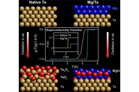
Magnesium protects tantalum, a promising material for making qubits
Scientists at the U.S. Department of Energy's (DOE) Brookhaven National Laboratory have discovered that adding a layer of magnesium improves the properties of tantalum, a superconducting material that shows great promise for building qubits, the basis of quantum computers. As described in a paper published in the journal Advanced Materials, a thin layer of magnesium keeps tantalum from oxidizing, improves its purity, and raises the temperature at which it operates as a superconductor. All three may increase tantalum's ability to hold onto quantum information in qubits. This work builds on earlier studies in which a team from Brookhaven's Center for Functional Nanomaterials (CFN), Brookhaven's National Synchrotron Light Source II (NSLS-II), and Princeton University sought to understand the tantalizing characteristics of tantalum, and then worked with scientists in Brookhaven's Condensed Matter Physics & Materials Science (CMPMS) Department and theorists at DOE's Pacific Northwest National Laboratory (PNNL) to reveal details about how the material oxidizes.
Read more.
#Materials Science#Science#Magnesium#Tantalum#Quantum mechanics#Quantum computing#Oxidation#Superconductors#Superconductivity
11 notes
·
View notes
Text
One of my cats has 2 sleeping positions, spread eagle, or perfect circle


#the first one she knocked over laundry lol#luckily it was already dirty but cmpm love#i gotta wash that#cats#caturday#fat cat
158 notes
·
View notes
Photo

Diseñamos tu sitio web, sin importar que tipo de página necesites o que harás con ella. Desarrollamos tu sitio web para emprendedores, pequeñas y grandes empresas, adaptables a pc, tabletas, móviles. Coméntanos que estás buscando y te ayudamos. WhatsApp: 6297-5269 Llamar a: 62975269 Correo: [email protected] Sitio web: https://debrau.com Escribir al directo Mensajes en comentarios #webdesignagency #tiendaonlinepanama #paginasweb #webdevelopment #landingpage #diseñoweb #diseñadoresweb #wordpress #diseñodepaginaweb #debraudesignstudio #carritodecompra #pasareladepago https://www.instagram.com/p/CMpm-z5hGZ3/?igshid=wvbo8j7k5tlh
#webdesignagency#tiendaonlinepanama#paginasweb#webdevelopment#landingpage#diseñoweb#diseñadoresweb#wordpress#diseñodepaginaweb#debraudesignstudio#carritodecompra#pasareladepago
1 note
·
View note
Photo

New Uniform? ✌🏼😅 #CMPM #CasinoMarketing #PremiumMarketing
0 notes
Link
http://blog.tiching.com/movil-en-el-aula-al-abordaje/?utm_content=CMPM%C3%B3vilEnElAula&utm_medium=referral&utm_campaign=cm&utm_source=twitter
@theinnovativeteacher
#propuestasTIC #móvil #aulas
1 note
·
View note
Text
Gold in limbo between solid and melted states
https://sciencespies.com/physics/gold-in-limbo-between-solid-and-melted-states/
Gold in limbo between solid and melted states


A schematic of the experimental setup for the time-resolved X-ray diffraction studies on the polycrystalline gold thin films. The sample is mounted perpendicular to the XFEL beam. A laser “pump” excites the sample, and then an X-ray pulse “probe” monitors the laser-induced changes at different time delays. The inset shows the X-ray diffraction patterns generated for the 300-nanometer film 50 picoseconds before and 100, 220, and 390 picoseconds after laser excitation. Credit: Brookhaven National Laboratory
If you heat a solid material enough, the thermal energy (latent heat) causes the material’s molecules begin to break apart, forming a liquid. One of the most familiar examples of this phase transition from a well-ordered solid to less-ordered liquid state is ice turning into water.
Though melting is a fundamental process of matter, scientists have not been fully able to understand how it works at a microscopic level, owing to the lack of research capabilities with sufficient time resolution. However, the advent of X-ray free-electron lasers (XFELs) in the past decade is making the study of the mechanism of melting, as well as other ultrafast atomic-scale dynamics, possible. These instruments use free (unbound) electrons to generate femtosecond (one-quadrillionth of a second) pulses of light in the X-ray energy region. Compared with X-ray synchrotrons, XFELs have X-ray pulses of a much shorter duration and higher intensity.
Now, a team of international scientists has used one of these instruments—the Pohang Accelerator Laboratory XFEL (PAL-XFEL) in South Korea—to monitor the melting of nanometer-thick gold films made up of lots of very tiny crystals oriented in various directions. They used an ultrashort X-ray pulse (“probe”) to monitor the structural changes following the excitation of these polycrystalline gold thin films by a femtosecond laser (“pump”), which induces melting. When the X-ray pulse strikes the gold, the X-ray beam gets diffracted in a pattern that is characteristic of the material’s crystal structure. By collecting X-ray diffraction images at different pump-probe time delays on picosecond (one-trillionth of a second) scales, they were able to take “snapshots” as melting began and progressed in the gold thin films. Changes in the diffraction patterns over time revealed the dynamics of crystal disordering. The scientists selected gold for this study because it diffracts x-rays very strongly and has a well-defined solid-to-liquid transition.
The X-ray diffraction patterns revealed that melting is inhomogeneous (nonuniform). In a paper published online in the Jan. 17 issue of Science Advances, scientists proposed that this melting likely originates at the interfaces where crystals of different orientations meet (imperfections called grain boundaries) and then propagates into the small crystalline regions (grains). In other words, the grain boundaries start melting before the rest of the crystal.
“Scientists believed that melting in polycrystalline materials occurs preferentially at surfaces and interfaces, but before XFEL the progression of melting as a function of time was unknown,” said co-corresponding author Ian Robinson, leader of the X-ray Scattering Group in the Condensed Matter Physics and Materials Science (CMPMS) Division at the U.S. Department of Energy’s (DOE) Brookhaven National Laboratory. “It was known that the laser generates “hot” (energetic) electrons, which cause melting when they transfer their energy to the crystal. The idea that this energy transfer process happens preferentially at grain boundaries and thus is not uniform has never been proposed until now.”

Brookhaven Lab physicists (from left to right) Ian Robinson, Tadesse Assefa, Ming Lu, Emil Bozin, and Simon Billinge at the Center for Functional Nanomaterials cleanroom, where they fabricated polycrystalline gold films of 50-, 100-, and 300-nanometer thickness. The team used time-resolved x-ray diffraction to understand the mechanism of melting in films excited by a laser that emits optical pulses with an extremely short duration. Their analysis of the X-ray diffraction images revealed that melting (induced by the laser) starts in one place and then moves into another location. Credit: Brookhaven National Laboratory
“The mechanism of laser-induced melting is important to consider for micromachining of precision parts used in aerospace, automotive, and other industries,” added first author Tadesse Assefa, a postdoc in Robinson’s group. “The way the laser couples to the material is different depending on the pulse duration of the laser. For example, the ultrashort pulses of femtosecond lasers seem to be better than the longer pulses of nanosecond lasers for making clean cuts such as drilling holes.”
For their experiment, the scientists first fabricated thin films of varying thickness (50, 100, and 300 nanometers) at the Center for Functional Nanomaterials (CFN)—a DOE Office of Science User Facility at Brookhaven. Here, in the CFN Nanofabrication Facility, they performed electron-beam evaporation, a deposition technique that uses electrons to condense the desired material onto a substrate. The ultraclean environment of this facility enabled them to create gold films of uniform thickness over a large sample area.
At PAL-XFEL, they conducted time-resolved X-ray diffraction on these films over a range of laser power levels. Software developed by staff in Brookhaven Lab’s Computational Science Initiative handled the high-throughput analysis of the terabytes of data generated as a detector collected the diffraction pattern images. The team then used software developed by scientists at Columbia Engineering to convert these images into linear graphs.
The plots revealed a double peak corresponding to a “hot” region undergoing melting (intermediate peak) and a relatively “cold” region (the rest of the crystal) which has yet to receive the latent heat of melting. Through electron coupling, heat goes to the grain boundaries and then conducts into the grains. This uptake of latent heat results in a band of melting material sandwiched between two moving melt fronts. Over time, this band becomes larger.

An illustration of grain boundary locations (points where lines intersect) in a polycrystalline gold thin film. The zoomed-in view shows how a melt front created at these boundaries propagates into the grains after the film is excited with an optical laser. Credit: Brookhaven National Laboratory
“One melt front is between a solid and melting region, and the other between a melting and liquid region,” explained Robinson.
Next, the team plans to confirm their two-front model by reducing the size of the grains (thereby increasing the number of grain boundaries) so they can reach the end of the melting process. Because melting occurs as a wave traversing the crystal grains at a relatively slow speed (30 meters per second), it takes longer than the timing range of the instrument (500 picoseconds) to cross big grains.
They would also like to look at other metals, alloys (mixtures of several metals or a metal combined with other elements), and catalytically relevant materials, in which grain boundaries are involved in chemical reactions.
“This study represents the very beginning of how we build an understanding of the mechanism of melting,” said Assefa. “By performing these experiments using different materials, we will be able to determine if our model is generalizable.”
Explore further
Atomic movie of melting gold could help design materials for future fusion reactors
More information: Tadesse A. Assefa et al, Ultrafast x-ray diffraction study of melt-front dynamics in polycrystalline thin films, Science Advances (2020). DOI: 10.1126/sciadv.aax2445
Provided by Brookhaven National Laboratory
Citation: Gold in limbo between solid and melted states (2020, March 2) retrieved 2 March 2020 from https://phys.org/news/2020-03-gold-limbo-solid-states.html
This document is subject to copyright. Apart from any fair dealing for the purpose of private study or research, no part may be reproduced without the written permission. The content is provided for information purposes only.
#Physics
1 note
·
View note
Photo

Making a movie of nanocrystal structural evolution
When you rapidly turn the pages of a flipbook, the series of static images look like they are moving. Scientists recently applied a similar principle to capture how the structure of a material changes over extremely short time scales—mere trillionths of a second or faster. To record this atomic-scale motion, they needed a special instrument housed at the U.S. Department of Energy's (DOE) Brookhaven National Laboratory.
"This ultrafast electron difraction instrument, which has electron beams with an energy of one million electron volts, was designed and made in house," said Jing Tao, a physicist in Brookhaven Lab's Condensed Matter Physics and Materials Science (CMPMS) Department and corresponding author on the Applied Physics Letters paper reporting the work. "We collaborated with the Lab's Accelerator Test Facility to ensure that temperature, humidity, and other environmental conditions remained stable and that the instrument was properly aligned."
Today's electron microscopes can resolve single atoms, but typically only at exposure times on the order of seconds. However, atoms move much more quickly than that.
"We are looking at structural dynamics that happen within hundreds of femtoseconds to a few picoseconds," said first author Junjie Li, a physicist in the CMPMS Department. "For reference, one femtosecond is equivalent to one quadrillionth of a second."
Read more.
#Materials Science#Science#Nanocrystals#Nanotechnology#Crystals#Copper sulfide#Copper#Sulfides#Crystal structure#Materials Characterization
48 notes
·
View notes
Photo

💓💓 Sign up for our email list for 20% off, link in bio to shop🛍 (at Jacksonville, Florida) https://www.instagram.com/p/Cmpm-x4Mfzp/?igshid=NGJjMDIxMWI=
0 notes
Photo

at Open Door Church https://www.instagram.com/p/Cmpm-XbromZ/?igshid=NGJjMDIxMWI=
0 notes
Photo

Cozy draws 😜 https://www.instagram.com/p/CmpM-4fuGWCf-YWc2ldGw5IsXeHUyzj-0oIioc0/?igshid=NGJjMDIxMWI=
0 notes
Photo
#holidays #2023 #family #love #italy #rome #champions #argentina #fifaworldcup #day2 #unsttopable 🇦🇷🇭🇺🦾🎬🎼⭐️🇦🇷🏆♥️🙏🏻⚽️🏆🏆🏆🚀🚀🚀 #messi #qatar #fifa #incantodiluci (at Incanto Di Luci) https://www.instagram.com/p/CmpM-MRLP0RCi2oeB1-DE-FioxZKFlXP3LcJPY0/?igshid=NGJjMDIxMWI=
#holidays#2023#family#love#italy#rome#champions#argentina#fifaworldcup#day2#unsttopable#messi#qatar#fifa#incantodiluci
0 notes
Photo

RNS https://www.instagram.com/p/CmPm-iEPqTo/?igshid=NGJjMDIxMWI=
0 notes
Photo

🌅🌊🌤️✔️ #sunsets #sunset #sunsetphotography #nature #sunsetlovers #sky #pics #sunsetlover #photography #ig #sunrise #naturephotography #landscape #photooftheday #captures #clouds #travel #sun #love #landscapephotography #beach #beautiful #travelphotography #instagood #naturelovers #vision #photo #picoftheday #sea #sunsetporn https://www.instagram.com/p/CmPm-91jRzj/?igshid=NGJjMDIxMWI=
#sunsets#sunset#sunsetphotography#nature#sunsetlovers#sky#pics#sunsetlover#photography#ig#sunrise#naturephotography#landscape#photooftheday#captures#clouds#travel#sun#love#landscapephotography#beach#beautiful#travelphotography#instagood#naturelovers#vision#photo#picoftheday#sea#sunsetporn
1 note
·
View note