#double circuit transmission line
Text
Powering Progress: Khurkot-New Butwal Transmission Line Enters Testing Phase
The Khurkot-New Butwal section of the Khurkot-New Butwal Transmission Line has been successfully tested. Following the completion of the section under the 220kV national pride Kaligandaki corridor project, charging started from 27 September.
The test of the 220 kV double circuit transmission line at a length of around 90 kms from the Khurkot substation at Khurkot of Kushma Municipality-2 in…

View On WordPress
#Asian Development Bank#Butwal substation#double circuit transmission line#Kaligandaki corridor project#Kaligandaki Corridor transmission line#Khurkot of Kushma#Khurkot substation#Khurkot-New Butwal sector#Khurkot-New Butwal Transmission Line#MVA transformer#Myagdi district#Nepal Electricity Authority#New Butwal substation#Parbat district#Sunawal Municipality
0 notes
Text
Magnetism 🧲 🍩 ⚛️ is God's building blocks of creation
It is NOT limited to the metal you see on your refrigerator. It's a neat trick / attribute, but it's not magnetism's original function in the biology of nature.
Dielectric inertial plane = The Electro-Static Equator within magnetism.
What he's saying, is when the space from end to end becomes to great, the magnetic geometry will not exist as it's usual Torus 🍩 ⚛️.
It then propagates in a DOUBLE HELIX 🧬 Phi-llotaxis 🌻 propagation, like a transmission line, or Light. DNA also.
Doesn't matter WHAT is propagating through the Air / Aer / Ether, SunLight or Energy transmission.
Energy is Energy & it propagates the same. In a coaxeal circuit, torodial vortex like manner.
Occult cabal run mainstream science's foundation is built upon their understanding of Light -> Conciousness
Their foundation to brainwash masses is based upon WHAT we're allowed to learn
They LIE to us as they wave symbolism -> Knowledge in our faces on Tel-a-vision
This is all explained in the Book of Enoch which was removed from the Bible because the powers that be don't want you to know about it.🤔
#pay attention#educate yourself#educate yourselves#reeducate yourself#knowledge is power#reeducate yourselves#think for yourself#think for yourselves#think about it#do your homework#do your research#do your own research#question everything#ask yourself questions#ask yourself#earth#flat earth
118 notes
·
View notes
Text
Global Top 3 Companies Accounted for 81% of total FPC for Power Battery market (QYResearch, 2021)
Flexible circuit board (FPC, Flexible Printed Circuit) is a circuit board made of flexible copper clad laminate as the base material. It is used as a medium for signal transmission in the connection of electronic products. Lightweight and flexible process. FPC can generally be divided into single-layer FPC, double-layer FPC, and multi-layer FPC. The functions of the power battery management system FPC mainly include: (1) monitor the voltage and temperature of the new energy power battery cells; (2) connect data acquisition and transmission and have its own overcurrent protection function; (3) protect the automotive power battery cells, the abnormal short circuit is automatically disconnected. Mainly used on the power square battery BMS, the general dosage is 3-70 pieces, instead of the traditional copper collection line.

According to the new market research report “Global FPC for Power Battery Market Report 2023-2029”, published by QYResearch, the global FPC for Power Battery market size is projected to reach USD 0.11 billion by 2029, at a CAGR of 33.8% during the forecast period.
Figure. Global FPC for Power Battery Market Size (US$ Million), 2018-2029

Above data is based on report from QYResearch: Global FPC for Power Battery Market Report 2023-2029 (published in 2023). If you need the latest data, plaese contact QYResearch..
Figure. Global FPC for Power Battery Top 3 Players Ranking and Market Share (Ranking is based on the revenue of 2022, continually updated)

Above data is based on report from QYResearch: Global FPC for Power Battery Market Report 2023-2029 (published in 2023). If you need the latest data, plaese contact QYResearch.
The global key manufacturers of FPC for Power Battery include YiDong Electronics Technology, Dongguan Guixiang, etc. In 2022, the global top three players had a share approximately 81.0% in terms of revenue.
About QYResearch
QYResearch founded in California, USA in 2007.It is a leading global market research and consulting company. With over 16 years’ experience and professional research team in various cities over the world QY Research focuses on management consulting, database and seminar services, IPO consulting, industry chain research and customized research to help our clients in providing non-linear revenue model and make them successful. We are globally recognized for our expansive portfolio of services, good corporate citizenship, and our strong commitment to sustainability. Up to now, we have cooperated with more than 60,000 clients across five continents. Let’s work closely with you and build a bold and better future.
QYResearch is a world-renowned large-scale consulting company. The industry covers various high-tech industry chain market segments, spanning the semiconductor industry chain (semiconductor equipment and parts, semiconductor materials, ICs, Foundry, packaging and testing, discrete devices, sensors, optoelectronic devices), photovoltaic industry chain (equipment, cells, modules, auxiliary material brackets, inverters, power station terminals), new energy automobile industry chain (batteries and materials, auto parts, batteries, motors, electronic control, automotive semiconductors, etc.), communication industry chain (communication system equipment, terminal equipment, electronic components, RF front-end, optical modules, 4G/5G/6G, broadband, IoT, digital economy, AI), advanced materials industry Chain (metal materials, polymer materials, ceramic materials, nano materials, etc.), machinery manufacturing industry chain (CNC machine tools, construction machinery, electrical machinery, 3C automation, industrial robots, lasers, industrial control, drones), food, beverages and pharmaceuticals, medical equipment, agriculture, etc.
0 notes
Text
RVNL and Salasar Techno Engineering Secure Transmission Project in Rwanda
Rail Vikas Nigam Limited (RVNL) and Salasar Techno Engineering have emerged as the Lowest Bidder (L1) for a significant transmission project in Rwanda. This development, disclosed under Regulation 30 of the SEBI (LODR) Regulations, 2015, marks a significant milestone for the joint venture between these two entities.
The project, awarded by Energy Development Corporation Limited (EDCL), entails the "Plant Design, Supply and Installation of 45.8 km, 110KV Double Circuit Rukarara-Huye-Gisagara Transmission Lines." This endeavor underscores the commitment of RVNL and Salasar Techno Engineering to contribute to the development of robust infrastructure, not only in India but also on the international stage.
According to the declaration as per SEBI Circular No. SEBI/HO/CFD-PoD-1/P/CIR/2023/123 dated July 13, 2023, the project involves several key aspects:
Name of the entity awarding the order: Energy Development Corporation Limited (EDCL)
Nature of the contract: Plant Design, Supply, and Installation of transmission lines
Domestic or international: International
Timeframe for execution: 18 months
Cost of the project: USD 7,152,236.59
This project signifies a strategic move by RVNL and Salasar Techno Engineering to expand their presence in the global infrastructure market. With their combined expertise and commitment to excellence, they are poised to deliver high-quality infrastructure solutions that meet the evolving needs of the communities they serve.
As the project progresses, it is expected to not only enhance Rwanda's power transmission capabilities but also foster economic growth and development in the region. RVNL and Salasar Techno Engineering's successful bid for this project reaffirms their position as leaders in the infrastructure sector and sets the stage for future collaborations and endeavors in the international arena.
0 notes
Text
3D reflectors help boost data rate in wireless communications - Technology Org
New Post has been published on https://thedigitalinsider.com/3d-reflectors-help-boost-data-rate-in-wireless-communications-technology-org/
3D reflectors help boost data rate in wireless communications - Technology Org
The next generation of wireless communication not only requires greater bandwidth at higher frequencies – it also needs a little extra time.
[embedded content]
Cornell researchers have developed a semiconductor chip that adds a necessary time delay so signals sent across multiple arrays can align at a single point in space and without disintegrating. The approach will enable ever-smaller devices to operate at the higher frequencies needed for future 6G communication technology.
The team’s paper, “Ultra-Compact Quasi-True-Time-Delay for Boosting Wireless Channel Capacity,” was published in Nature. Bal Govind, an electrical and computer engineering doctoral student, is the lead author.
Most current wireless communications, such as 5G phones, operate at frequencies below 6 gigahertz (GHz). Technology companies have been aiming to develop a new wave of 6G cellular communications that use frequencies above 20 GHz, where there is more available bandwidth, which means more data can flow and at a faster rate. 6G is expected to be 100 times faster than 5G.
However, since data loss through the environment is greater at higher frequencies, one crucial factor is how the data is relayed. Instead of relying on a single transmitter and a single receiver, most 5G and 6G technologies use a more energy-efficient method: a series of phased arrays of transmitters and receivers.
“Every frequency in the communication band goes through different time delays,” Govind said. “The problem we’re addressing is decades old – that of transmitting high-bandwidth data in an economical manner so signals of all frequencies line up at the right place and time.”
“It’s not just building something with enough delay, it’s building something with enough delay where you still have a signal at the end,” said senior author Alyssa Apsel, the IBM Professor of Engineering and director of electrical and computer engineering in Cornell Engineering. “The trick is that we were able to do it without enormous loss.”
The computer chip designed by Bal Govind and team. Image credit: Ryan Young/Cornell University
This delay has previously been produced by phase-shifting circuits, but they can handle only so much data. That is a particular problem for wideband signals, in which the highest and the lowest frequencies can fall out of phase, causing the signal to blur, a phenomenon known as “beam squint.” And building time delays into a tiny chip that can fit in a smart phone is no small task.
“Most of the way that time delay is constructed is literally by using a long wire that will enable you to delay a signal from point A to point B. And we need that delay to be tunable so that we can reroute this beam to different locations. We want it to be reconfigurable,” Apsel said.
Govind worked with postdoctoral researcher and co-author Thomas Tapen to design a complementary metal-oxide-semiconductor (CMOS) that could tune a time delay over an ultra-broad bandwidth of 14 GHz, with as high as 1 degree of phase resolution.
“Since the aim of our design was to pack as many of these delay elements as possible,” Govind said, “we imagined what it would be like to wind the path of the signal in three-dimensional waveguides and bounce signals off of them to cause delay, instead of laterally spreading wavelength-long wires across the chip.”
The team engineered a series of these 3D reflectors strung together to form a “tunable transmission line.”
The resulting integrated circuit occupies a 0.13-square-millimeter footprint that is smaller than phase shifters yet nearly doubles the channel-capacity – i.e., data rate – of conventional wireless arrays. And by boosting the projected data rate, the chip could provide faster service, getting more data to cellphone users.
“The big problem with phased arrays is this tradeoff between trying to make these things small enough to put on a chip and maintain efficiency,” Apsel said. “The answer that most of the industry has landed on is, ‘Well, we can’t do time delay, so we’re going to do phase delay.’ And that fundamentally limits how much information you can transmit and receive. They just sort of take that hit.
“I think one of our major innovations is really the question: Do you need to build it this way?” Apsel said. “If we can boost the channel capacity by a factor of 10 by changing one component, that is a pretty interesting game-changer for communications.”
Source: Cornell University
You can offer your link to a page which is relevant to the topic of this post.
#3d#3D image#5G#6G#6G technology#approach#Arrays#blur#Building#channel#communication#communications#Companies#computer#data#data loss#Delay#Design#devices#doubles#efficiency#energy#engineering#Environment#factor#form#Fundamental physics news#Future#game#how
1 note
·
View note
Text
Solution Manuals For Diode Lasers and Photonic Integrated Circuits 2nd Edition By Larry A. Coldren

Solution Manuals For Diode Lasers and Photonic Integrated Circuits 2nd Edition By Larry A. Coldren
TABLE OF CONTENTS
Preface xvii
Acknowledgments xxi
List of Fundamental Constants xxiii
1 Ingredients 1
1.1 Introduction 1
1.2 Energy Levels and Bands in Solids 5
1.3 Spontaneous and Stimulated Transitions: The Creation of Light 7
1.4 Transverse Confinement of Carriers and Photons in Diode Lasers: The Double Heterostructure 10
1.5 Semiconductor Materials for Diode Lasers 13
1.6 Epitaxial Growth Technology 20
1.7 Lateral Confinement of Current, Carriers, and Photons for Practical Lasers 24
1.8 Practical Laser Examples 31
References 39
Reading List 40
Problems 40
2 A Phenomenological Approach to Diode Lasers 45
2.1 Introduction 45
2.2 Carrier Generation and Recombination in Active Regions 46
2.3 Spontaneous Photon Generation and LEDs 49
2.4 Photon Generation and Loss in Laser Cavities 52
2.5 Threshold or Steady-State Gain in Lasers 55
2.6 Threshold Current and Power Out Versus Current 60
2.6.1 Basic P–I Characteristics 60
2.6.2 Gain Models and Their Use in Designing Lasers 64
2.7 Relaxation Resonance and Frequency Response 70
2.8 Characterizing Real Diode Lasers 74
2.8.1 Internal Parameters for In-Plane Lasers: ‹αi›, ηi , and g versus J 75
2.8.2 Internal Parameters for VCSELs: ηi and g versus J, ‹αi›, and αm 78
2.8.3 Efficiency and Heat Flow 79
2.8.4 Temperature Dependence of Drive Current 80
2.8.5 Derivative Analysis 84
References 86
Reading List 87
Problems 87
3 Mirrors and Resonators for Diode Lasers 91
3.1 Introduction 91
3.2 Scattering Theory 92
3.3 S and T Matrices for Some Common Elements 95
3.3.1 The Dielectric Interface 96
3.3.2 Transmission Line with No Discontinuities 98
3.3.3 Dielectric Segment and the Fabry–Perot Etalon 100
3.3.4 S-Parameter Computation Using Mason’s Rule 104
3.3.5 Fabry–Perot Laser 105
3.4 Three- and Four-Mirror Laser Cavities 107
3.4.1 Three-Mirror Lasers 107
3.4.2 Four-Mirror Lasers 111
3.5 Gratings 113
3.5.1 Introduction 113
3.5.2 Transmission Matrix Theory of Gratings 115
3.5.3 Effective Mirror Model for Gratings 121
3.6 Lasers Based on DBR Mirrors 123
3.6.1 Introduction 123
3.6.2 Threshold Gain and Power Out 124
3.6.3 Mode Selection in DBR-Based Lasers 127
3.6.4 VCSEL Design 128
3.6.5 In-Plane DBR Lasers and Tunability 135
3.6.6 Mode Suppression Ratio in DBR Laser 139
3.7 DFB Lasers 141
3.7.1 Introduction 141
3.7.2 Calculation of the Threshold Gains and Wavelengths 143
3.7.3 On Mode Suppression in DFB Lasers 149
References 151
Reading List 151
Problems 151
4 Gain and Current Relations 157
4.1 Introduction 157
4.2 Radiative Transitions 158
4.2.1 Basic Definitions and Fundamental Relationships 158
4.2.2 Fundamental Description of the Radiative Transition Rate 162
4.2.3 Transition Matrix Element 165
4.2.4 Reduced Density of States 170
4.2.5 Correspondence with Einstein’s Stimulated Rate Constant 174
4.3 Optical Gain 174
4.3.1 General Expression for Gain 174
4.3.2 Lineshape Broadening 181
4.3.3 General Features of the Gain Spectrum 185
4.3.4 Many-Body Effects 187
4.3.5 Polarization and Piezoelectricity 190
4.4 Spontaneous Emission 192
4.4.1 Single-Mode Spontaneous Emission Rate 192
4.4.2 Total Spontaneous Emission Rate 193
4.4.3 Spontaneous Emission Factor 198
4.4.4 Purcell Effect 198
4.5 Nonradiative Transitions 199
4.5.1 Defect and Impurity Recombination 199
4.5.2 Surface and Interface Recombination 202
4.5.3 Auger Recombination 211
4.6 Active Materials and Their Characteristics 218
4.6.1 Strained Materials and Doped Materials 218
4.6.2 Gain Spectra of Common Active Materials 220
4.6.3 Gain versus Carrier Density 223
4.6.4 Spontaneous Emission Spectra and Current versus Carrier Density 227
4.6.5 Gain versus Current Density 229
4.6.6 Experimental Gain Curves 233
4.6.7 Dependence on Well Width, Doping, and Temperature 234
References 238
Reading List 240
Problems 240
5 Dynamic Effects 247
5.1 Introduction 247
5.2 Review of Chapter 2 248
5.2.1 The Rate Equations 249
5.2.2 Steady-State Solutions 250
Case (i): Well Below Threshold 251
Case (ii): Above Threshold 252
Case (iii): Below and Above Threshold 253
5.2.3 Steady-State Multimode Solutions 255
5.3 Differential Analysis of the Rate Equations 257
5.3.1 Small-Signal Frequency Response 261
5.3.2 Small-Signal Transient Response 266
5.3.3 Small-Signal FM Response or Frequency Chirping 270
5.4 Large-Signal Analysis 276
5.4.1 Large-Signal Modulation: Numerical Analysis of the Multimode Rate Equations 277
5.4.2 Mode Locking 279
5.4.3 Turn-On Delay 283
5.4.4 Large-Signal Frequency Chirping 286
5.5 Relative Intensity Noise and Linewidth 288
5.5.1 General Definition of RIN and the Spectral Density Function 288
5.5.2 The Schawlow–Townes Linewidth 292
5.5.3 The Langevin Approach 294
5.5.4 Langevin Noise Spectral Densities and RIN 295
5.5.5 Frequency Noise 301
5.5.6 Linewidth 303
5.6 Carrier Transport Effects 308
5.7 Feedback Effects and Injection Locking 311
5.7.1 Optical Feedback Effects—Static Characteristics 311
5.7.2 Injection Locking—Static Characteristics 317
5.7.3 Injection and Feedback Dynamic Characteristics and Stability 320
5.7.4 Feedback Effects on Laser Linewidth 321
References 328
Reading List 329
Problems 329
6 Perturbation, Coupled-Mode Theory, Modal Excitations, and Applications 335
6.1 Introduction 335
6.2 Guided-Mode Power and Effective Width 336
6.3 Perturbation Theory 339
6.4 Coupled-Mode Theory: Two-Mode Coupling 342
6.4.1 Contradirectional Coupling: Gratings 342
6.4.2 DFB Lasers 353
6.4.3 Codirectional Coupling: Directional Couplers 356
6.4.4 Codirectional Coupler Filters and Electro-optic Switches 370
6.5 Modal Excitation 376
6.6 Two Mode Interference and Multimode Interference 378
6.7 Star Couplers 381
6.8 Photonic Multiplexers, Demultiplexers and Routers 382
6.8.1 Arrayed Waveguide Grating De/Multiplexers and Routers 383
6.8.2 Echelle Grating based De/Multiplexers and Routers 389
6.9 Conclusions 390
References 390
Reading List 391
Problems 391
7 Dielectric Waveguides 395
7.1 Introduction 395
7.2 Plane Waves Incident on a Planar Dielectric Boundary 396
7.3 Dielectric Waveguide Analysis Techniques 400
7.3.1 Standing Wave Technique 400
7.3.2 Transverse Resonance 403
7.3.3 WKB Method for Arbitrary Waveguide Profiles 410
7.3.4 2-D Effective Index Technique for Buried Rib Waveguides 418
7.3.5 Analysis of Curved Optical Waveguides using Conformal Mapping 421
7.3.6 Numerical Mode Solving Methods for Arbitrary Waveguide Profiles 424
7.4 Numerical Techniques for Analyzing PICs 427
7.4.1 Introduction 427
7.4.2 Implicit Finite-Difference Beam-Propagation Method 429
7.4.3 Calculation of Propagation Constants in a z–invariant Waveguide from a Beam Propagation Solution 432
7.4.4 Calculation of Eigenmode Profile from a Beam Propagation Solution 434
7.5 Goos–Hanchen Effect and Total Internal Reflection Components 434
7.5.1 Total Internal Reflection Mirrors 435
7.6 Losses in Dielectric Waveguides 437
7.6.1 Absorption Losses in Dielectric Waveguides 437
7.6.2 Scattering Losses in Dielectric Waveguides 438
7.6.3 Radiation Losses for Nominally Guided Modes 438
References 445
Reading List 446
Problems 446
8 Photonic Integrated Circuits 451
8.1 Introduction 451
8.2 Tunable, Widely Tunable, and Externally Modulated Lasers 452
8.2.1 Two- and Three-Section In-plane DBR Lasers 452
8.2.2 Widely Tunable Diode Lasers 458
8.2.3 Other Extended Tuning Range Diode Laser Implementations 463
8.2.4 Externally Modulated Lasers 474
8.2.5 Semiconductor Optical Amplifiers 481
8.2.6 Transmitter Arrays 484
8.3 Advanced PICs 484
8.3.1 Waveguide Photodetectors 485
8.3.2 Transceivers/Wavelength Converters and Triplexers 488
8.4 PICs for Coherent Optical Communications 491
8.4.1 Coherent Optical Communications Primer 492
8.4.2 Coherent Detection 495
8.4.3 Coherent Receiver Implementations 495
8.4.4 Vector Transmitters 498
References 499
Reading List 503
Problems 503
Appendices
1 Review of Elementary Solid-State Physics 509
A1.1 A Quantum Mechanics Primer 509
A1.1.1 Introduction 509
A1.1.2 Potential Wells and Bound Electrons 511
A1.2 Elements of Solid-State Physics 516
A1.2.1 Electrons in Crystals and Energy Bands 516
A1.2.2 Effective Mass 520
A1.2.3 Density of States Using a Free-Electron (Effective Mass) Theory 522
References 527
Reading List 527
2 Relationships between Fermi Energy and Carrier Density and Leakage 529
A2.1 General Relationships 529
A2.2 Approximations for Bulk Materials 532
A2.3 Carrier Leakage Over Heterobarriers 537
A2.4 Internal Quantum Efficiency 542
References 544
Reading List 544
3 Introduction to Optical Waveguiding in Simple Double-Heterostructures 545
A3.1 Introduction 545
A3.2 Three-Layer Slab Dielectric Waveguide 546
A3.2.1 Symmetric Slab Case 547
A3.2.2 General Asymmetric Slab Case 548
A3.2.3 Transverse Confinement Factor, Γx 550
A3.3 Effective Index Technique for Two-Dimensional Waveguides 551
A3.4 Far Fields 555
References 557
Reading List 557
4 Density of Optical Modes, Blackbody Radiation, and Spontaneous Emission Factor 559
A4.1 Optical Cavity Modes 559
A4.2 Blackbody Radiation 561
A4.3 Spontaneous Emission Factor, βsp 562
Reading List 563
5 Modal Gain, Modal Loss, and Confinement Factors 565
A5.1 Introduction 565
A5.2 Classical Definition of Modal Gain 566
A5.3 Modal Gain and Confinement Factors 568
A5.4 Internal Modal Loss 570
A5.5 More Exact Analysis of the Active/Passive Section Cavity 571
A5.5.1 Axial Confinement Factor 572
A5.5.2 Threshold Condition and Differential Efficiency 573
A5.6 Effects of Dispersion on Modal Gain 576
6 Einstein’s Approach to Gain and Spontaneous Emission 579
A6.1 Introduction 579
A6.2 Einstein A and B Coefficients 582
A6.3 Thermal Equilibrium 584
A6.4 Calculation of Gain 585
A6.5 Calculation of Spontaneous Emission Rate 589
Reading List 592
7 Periodic Structures and the Transmission Matrix 593
A7.1 Introduction 593
A7.2 Eigenvalues and Eigenvectors 593
A7.3 Application to Dielectric Stacks at the Bragg Condition 595
A7.4 Application to Dielectric Stacks Away from the Bragg Condition 597
A7.5 Correspondence with Approximate Techniques 600
A7.5.1 Fourier Limit 601
A7.5.2 Coupled-Mode Limit 602
A7.6 Generalized Reflectivity at the Bragg Condition 603
Reading List 605
Problems 605
8 Electronic States in Semiconductors 609
A8.1 Introduction 609
A8.2 General Description of Electronic States 609
A8.3 Bloch Functions and the Momentum Matrix Element 611
A8.4 Band Structure in Quantum Wells 615
A8.4.1 Conduction Band 615
A8.4.2 Valence Band 616
A8.4.3 Strained Quantum Wells 623
References 627
Reading List 628
9 Fermi’s Golden Rule 629
A9.1 Introduction 629
A9.2 Semiclassical Derivation of the Transition Rate 630
A9.2.1 Case I: The Matrix Element-Density of Final States Product is a Constant 632
A9.2.2 Case II: The Matrix Element-Density of Final States Product is a Delta Function 635
A9.2.3 Case III: The Matrix Element-Density of Final States Product is a Lorentzian 636
Reading List 637
Problems 638
10 Transition Matrix Element 639
A10.1 General Derivation 639
A10.2 Polarization-Dependent Effects 641
A10.3 Inclusion of Envelope Functions in Quantum Wells 645
Reading List 646
11 Strained Bandgaps 647
A11.1 General Definitions of Stress and Strain 647
A11.2 Relationship Between Strain and Bandgap 650
A11.3 Relationship Between Strain and Band Structure 655
References 656
12 Threshold Energy for Auger Processes 657
A12.1 CCCH Process 657
A12.2 CHHS and CHHL Processes 659
13 Langevin Noise 661
A13.1 Properties of Langevin Noise Sources 661
A13.1.1 Correlation Functions and Spectral Densities 661
A13.1.2 Evaluation of Langevin Noise Correlation Strengths 664
A13.2 Specific Langevin Noise Correlations 665
A13.2.1 Photon Density and Carrier Density Langevin Noise Correlations 665
A13.2.2 Photon Density and Output Power Langevin Noise Correlations 666
A13.2.3 Photon Density and Phase Langevin Noise Correlations 667
A13.3 Evaluation of Noise Spectral Densities 669
A13.3.1 Photon Noise Spectral Density 669
A13.3.2 Output Power Noise Spectral Density 670
A13.3.3 Carrier Noise Spectral Density 671
References 672
Problems 672
14 Derivation Details for Perturbation Formulas 675
Reading List 676
15 Multimode Interference 677
A15.1 Multimode Interference-Based Couplers 677
A15.2 Guided-Mode Propagation Analysis 678
A15.2.1 General Interference 679
A15.2.2 Restricted Multimode Interference 681
A15.3 MMI Physical Properties 682
A15.3.1 Fabrication 682
A15.3.2 Imaging Quality 682
A15.3.3 Inherent Loss and Optical Bandwidth 682
A15.3.4 Polarization Dependence 683
A15.3.5 Reflection Properties 683
Reference 683
16 The Electro-Optic Effect 685
References 692
Reading List 692
17 Solution of Finite Difference Problems 693
A17.1 Matrix Formalism 693
A17.2 One-Dimensional Dielectric Slab Example 695
Reading List 696
Index 697
Read the full article
0 notes
Text
Unveiling the advantages and disadvantages of Surface Mount Technology (SMT)
Introduction
Printed circuit board assembly, in particular, has significantly benefited from surface mount technology (SMT). SMT eliminates the requirement for drilled holes and manual insertion by mounting electronic components directly onto a PCB's surface. This technique offers several advantages, such as smaller and thinner PCBs, flexibility in design, reduced material costs, simplified automation, and high signal transmission capabilities.
Advantages of SMT in PCB Assembly
Ultra-Thin and Miniature PCBs
The size and weight of surface-mount components are significantly lower than their through-hole counterparts. Boards are smaller and thinner because their compactness makes better use of space on printed circuit boards. As a result, products can be designed to be more compact without compromising functionality or performance.
Flexibility
SMT provides great flexibility in terms of PCB materials and designs. It enables the use of flexible PCBs (flex PCBs) and rigid-flex PCBs that can bend or conform to specific shapes or spaces. This flexibility opens up opportunities for innovative designs while maintaining excellent electrical performance.
Lesser Expense on Materials and Cardboard
Unlike through-hole components that require manual insertion, SMD components can be automatically placed on the board using pick-and-place machines or automated assembly lines. This automation streamlines the production process, reduces labour costs, and improves efficiency.
Simplified Manufacturing Process
When compared to through-hole components, surface-mount devices (SMDs) can be automatically positioned on the board through the use of pick-and-place machines or automated assembly lines. Because of this automation, production is more streamlined, costs less to operate, and more efficient overall.
Frequency and High Signal Transmission
Fast signal transmission with less radio frequency interference is made possible using SMT components, which are compatible with high-density double-sided and multi-layer printed circuit board assembly. Additionally, SMT assemblies' lack of leads improves their resilience to vibration and guarantees dependable signal integrity.
Drawbacks of SMT for PCB Build-Up
High Initial Investment
Implementing SMT assembly requires investment in specialized equipment such as reflow ovens, solder paste screen printers, pick-and-place machines, and hot air rework stations. These machines can be costly but are essential for efficient and accurate assembly.
Difficult to Inspect
Due to the small sizes and numerous solder joints of most SMD components, inspection becomes challenging. Identifying defects or faults can be time-consuming, especially when dealing with complex packages like ball grid arrays (BGAs), where solder balls are located under the component.
Fragility
Comparing surface-mount components to their through-hole counterparts, SMD parts are more delicate and fragile. They can be easily damaged if mishandled or dropped during the manufacturing process or while in use. Special care must be taken to handle and package these components using anti-static measures in clean room environments.
Expensive Small Batch Production
Technical complexity necessitates skilled operators and specialized equipment, making prototyping or small-batch manufacture of SMT PCBs an expensive ordeal. Due to the high initial setup expenses, SMT technology may not be cost-effective for small volumes.
Limited Power Capabilities
Surface mount technology isn't suitable for all electrical components, active or passive, because of power constraints. Components generating high heat may not be suitable for surface mounting as it can cause solder melting and compromise the integrity of the connection.
Despite these challenges, SMT remains a highly recommended practice in the manufacturing industry due to its numerous benefits. It enables manufacturing efficiency, design flexibility, better performance in harsh conditions or high-frequency applications, and more compact devices without compromising functionality or performance attributes. With ongoing advancements and innovations in SMT technology aimed at addressing existing limitations and improving production processes further, we can expect to see continued growth and impact on the industry.
This Blog Originally Posted Here: https://www.pcbpower.us/blog/unveiling-the-advantages-and-disadvantages-of-surface-mount-technology
0 notes
Text
Insulated conductors
Insulated conductors are used in power transmission and distribution systems, in which a layer of non-conductive materials, such as: resin, plastic, silicone rubber, PVC, etc., is uniformly and sealingly wrapped around the periphery of the conductor to form an insulating layer to prevent the conductor from contacting the outside world causing leakage, short circuit, electric shock and other accidents, the inside of the insulated conductor is composed of a metal conductor, usually copper or aluminum, while the outer layer is a layer of insulating material.
Compared with ordinary wires, insulated wires have better electrical insulation properties, which can prevent current leakage and interference, thus improving the safety and reliability of the power system. Insulated conductors are commonly used in high-voltage lines in power transmission and distribution systems, such as transmission lines and cables in substations.
R stands for soft copper wire, V stands for polyvinyl chloride insulation, S stands for double twisted, B stands for flat, and P stands for shielded.
1, RV - polyvinyl chloride insulated single-core flexible wire, maximum operating temperature 65℃, minimum operating temperature -15℃, working voltage AC 250V, DC 500V, used as internal wiring of instruments and equipment.
2, RVB: parallel multi-stranded flexible wire (flat), like the phone line often used at home bare wire, but the core and RVV core consistent, the two cores are wrapped in parallel in the sheath, usually a sheath of two
3, RVS: twisted multi-stranded flexible wire, that is, the soft core of RVB torn, twisted. Usually two twisted pairs.
4、RVSP: twisted shielded wire.
5、RVVB: polyvinyl chloride sheathed flexible wire (flat type), standard GB/T 5023.5-2008/IEC 60227-5:2003.
6, RVV: multi-stranded flexible wire, that is, the core consists of multiple strands of copper wire, RVV wire is the most commonly used cable for weak electrical systems, the number of cores is variable, there are single, there are multiple, there is also a sheath outside. But there are no special requirements for the arrangement between the cores.
7, RVVP: copper-core PVC insulated shielded PVC sheathed flexible cable, also called electrical connection anti-interference flexible cable, rated voltage 250V/450V.
8, BVVR is a copper-core PVC insulated PVC sheathed flexible wire, with an outer sheath; BVR is a copper-core PVC insulated flexible wire, only the insulation layer, no outer sheath. Usually said double plastic wire refers to the BVV series, the first V refers to polyvinyl chloride insulation, the second V refers to polyvinyl chloride sheathing, if the BV series refers to the single plastic wire.
Commonly used insulated wires are as follows: 1:
1 rubber-insulated wire Model: BLX - aluminum-core rubber-insulated wire, BX - copper-core rubber-insulated wire.
2 polyvinyl chloride insulated wire (plastic wire) Model: BLV - aluminum-core plastic wire, BV - copper-core plastic wire.
Rubber cable Model: YHC - heavy-duty rubber cable, NYHF - agricultural neoprene dragging cable.
Rubber insulated wire has copper core, aluminum core, single core, double core and multi-core. Used for house wiring, working voltage generally does not exceed 5OO volts.
Insulated conductors come in various forms, including overhead insulated conductors and underground insulated cables. Overhead insulated conductors are transmitted through overhead power poles or cable bridges, while underground insulated cables are buried in underground pipes or tunnels to transmit power signals. Different insulated conductors are suitable for different power transmission and distribution scenarios and are selected as needed.

0 notes
Text
Utkarsh India Limited India's Leading Transmission Tower Manufacturers & Suppliers
Take a closer look at Utkarsh India's high-quality Powergrid-approved transmission line towers. Gain an in-depth understanding of our wide range of transmission tower offerings including single, double, and multi-circuit towers. These towers are suitable for Twin, Quad, and Hex conductor configurations. To watch the video, click here:
youtube
Website URL:
0 notes
Text
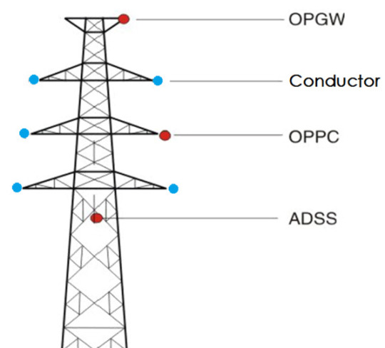
Do You Want to Understand the Difference Between ADSS and OPGW Fiber Optic Cable?
ADSS cable and OPGW cable are often used in power utilities and telecommunications nowadays.In this article, some differences between ADSS and OPGW cables will be discussed.

What are OPGW and ADSS Cables?
All-dielectric Self-supporting (ADSS) cable is a type of fiber optic cable that is strong enough to support itself between structures without using conductive metal elements.The cable is designed for aerial transmission and distribution power lines environments. As its name indicates, there are no metallic components and the cable does not require a support or messenger wire, so installation is achieved in a single pass.
Optical ground wire (OPGW), also known as optical fiber composite overhead ground wire is a dual-functioning cable performing the duties of a ground wire and also providing a path for the transmission of voice, video, or data signals.The cable is designed to be installed on transmission and distribution lines. The fibers are protected from environmental conditions (lightning, short circuit, loading) to ensure the reliability of signal transmission.
ADSS VS.OPGW Cables
ADSS or OPGW, when dealing with outdoor fiber cabling, might be tough sometimes due to the difference in cabling designs, features, environment, cost, and applications.Let's take look at the main differences between them.
Structure
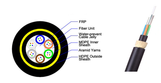
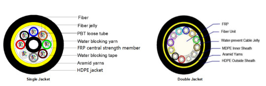
ADSS cable structure is mainly composed of central strength member, stranded loose tube, water blocking material, aramid yarn, and sheath. ADSS cable structure consists of 2 types: single jacket and double jacket.
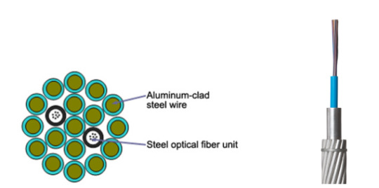
OPGW cable structure is mainly composed of an optical fiber unit (stainless steel tube, aluminum-clad stainless steel tube) , and metal mono-filament (aluminum-clad steel, aluminum alloy) peripheral reinforcement. There are 4 OPGW cable types: ACS (Aluminum clad stainless steel tube), stranded tube, central tube, and ACP (Aluminum clad PBT).

Features
ADSS cable can be installed without shutting off the power, large span lengths, good performance of tensile strength, lightweight and small diameter.
OPGW cable provide stainless-steel optical fiber unit with layer stranding structure, aluminum alloy wire and aluminum clad steel wire armored, coated with anti-corrosive grease between layers, heavy load capacity and long span installation.
Installation Position
The installation position is inconsistent - If the wires need to be rewired or replaced due to aging, it is more suitable to use OPGW cables than ADSS cables.Unlike OPGW optical cables, ADSS cables are more suitable for installation in the power distribution and transmission environment where the live wire is placed.

Installation Cost
The installation cost of OPGW cable is relatively high, and a lot of money needs to be invested at one time; while the installation cost of ADSS cable is relatively low, because it does not need to replace the electrical transmission line, and can also achieve free switching.
Applications
OPGW cable is used in the electric utility industry, transmission and distribution of power lines ( i.e., 500KV, 220KV, 110KV voltage grade lines), voice, video, data transmission, SCADA networks, ariel ground wires, and dark fiber leasing.
ADSS cable is used for telecommunications by power utilities, telcos, and private network groups, distribution and high voltage transmission lines, conductors, outdoor aerial self-supporting installation, enterprise OSP networks, broadband, FTTX networks, railways, long-distance communication, CATV, CCTV, computer networks system, ethernet LAN Network, outside plant campus backbone, etc.
Conclusion
ADSS cable is cheaper than OPGW cable and easy to install.However, OPGW cable has high voltage transmission efficiency, and can also be used for telecommunication transmission data to achieve the purpose of high-speed data transmission.Sun Telecom provides all ADSS and OPGW cable products and solutions to the global market.
1 note
·
View note
Text
Intriguing datum

Taken together, my data reveals the complexity by which inhibitory synapse organizers regulate brain function in a circuit specific and a cell-type specific manner. Particularly, Nlgn2-IgSF9b double deletion exacerbated the fear learning deficit in Nlgn2 KO mice, in contrast to the normalization of anxiety-like behavior reported previously in the double KO mice. use a physical datum of 1700 as the starting point because it was a. through their geometric completions, intriguing topological groups. Moreover, the modulation of Nlgn2 function by its interaction partner IgSF9b was also distinct between fear learning and anxiety. wheat production in physical units during the intriguing period of 1645-1761. a root group datum (with infinite Weyl group) the proof relies only on the. In contrast, mice lacking Nlgn2 from specific inhibitory neurons showed normal exploratory behavior using the same test. Unlike what I observed in fear learning, deletion of Nlgn2 from excitatory CAMKII neurons fully recapitulated the anxiety-like behavior of Nlgn2 KO mice in the open field test. While the reduction in fear learning in a mouse model with increased anxiety-like behavior is intriguing, I found that these two behaviors are controlled by effects of Nlgn2 on different cell types. This result was also supported by learning-dependent overactivation of VIP interneurons (INs) in the LA during FC retrieval. Particularly, deletion of Nlgn2 from vasoactive intestinal peptide (VIP) expressing inhibitory neurons, but not from Ca+2/Calmodulin-dependent protein kinase-II (CAMKII) expressing excitatory neurons, recapitulated the FC deficit in Nlgn2 KO. Using cell-type specific gene knockout approach, I found that the FC deficit in Nlgn2 KO was caused by lack of Nlgn2 from specific inhibitory neurons subtypes rather than excitatory neurons. It marks a new order of the development with simplicity intertwining with intriguing programs expressed on various datum lines on different dimensions. In these regions, a lack of activation in response to FC was detected in Nlgn2 KO compared to WT mice, in line with impaired plasticity required for fear memory formation. Using immediate-early gene expression assay to probe neuronal activation during FC retrieval, I detected dysregulated activation in Nlgn2 KO mice in brain regions that are involved in fear memory processing such as the lateral amygdala (LA), the medial prefrontal cortex (mPFC) and the auditory cortex (AuC). I observed a behavioral impairment measured at the level of short and long-term fear memory retrieval in Nlgn2 KO mice that was specific to auditory, but not contextual FC. Aiming to understand how Nlgn2 regulates the function and plasticity of emotional circuits, I characterized its role in fear learning using the Pavlovian fear conditioning (FC) paradigm. However, at the level of behavioral circuits, Nlgn2 knockout mice (Nlgn2 KO) exhibited phenotypes that were specifically related to the function of emotional circuits, such as anxiety-like behavior and cognitive impairments involving aversive emotional valence. Lack of Nlgn2 in mice produced a reduction in inhibitory synaptic transmission in many brain regions. Englisch Neuroligin-2 (Nlgn2) is a synaptic adhesion molecule that promotes the maturation and function of inhibitory synapses.
0 notes
Text
Superior Voltage Products plus the Direct Current Voltage Test

bare conductor transmission line
High voltage products require an intriguing mix of science together with engineering in order to tolerate the forces this that are applied to these. When moving big voltage electricity within the country, it is vital to enjoy equipment that can undergo the rigors which might be placed upon him or her. There is a range of superior voltage products which can be worth mentioning in this case. However , this is a brief summary for the reason that each individual component is obviously worth discussing in a very greater amount of characteristic.
bare conductor transmission line
There are a number of switchgear units which are built to be able to cope with extremely high voltages.
These include air-insulated switchgears, gas-insulated switchgears, as well as other hybrid switchgears which are designed for targeted purposes. Other merchandise worth mentioning comprise of generator circuit breakers, disconnectors, and means transformers.
Surge arrestors are a crucial equpiment when dealing with huge voltage electricity. For the reason that levels in a line can vary at times, a surge will cause a huge amount associated with damage to other power equipment, and can provide whole circuits difficult shut down. Surge arrestors are able to control your surge in order to steer clear of the damage that might have got occurred. Instrument transformers are utilized for a a number of applications, including income metering, insulation, combined with protection and manipulate services.
When experiencing insulation, long-rod insulators, made of silicone, are used on certain 550kV overhead power traces. Disconnectors also have various applications, and can come to be utilized on lines from about 72. 5kV up to massive 800kV. A few range of coil supplements that are manufactured through the electrical manufacturing organizations, in addition to the variety of various smaller components which were manufactured specifically to get over high voltages.
To get electrical engineers, an immediate current voltage examination is something that will have to be performed from time to time.
Consequently, these are pressure reports that are conducted concerning high voltage cables and wires. While many cables run on AC, for a lot of reasons the AIR COOLING testing is not likely, which is why DC trying out must take place. Most of the time, a DC evaluation will be comprised of one half wave rectification, and definately will typically make use of HV selenium rectifiers. It's likely you have heard about doubling and additionally multiplier circuits. These kind of circuits are used using some simple household devices, like in tv's, but also have excessive voltage applications.
1 note
·
View note
Text
RVNL-Salasar JV gets Rs 60 crore transmission project in Central Africa
In the bustling world of infrastructure development, a noteworthy joint venture between state-owned RVNL and private entity Salasar Techno Engineering has recently made headlines. The venture has clinched a significant transmission project valued at approximately Rs 60 crore in Rwanda, a central African nation known for its picturesque landscapes and burgeoning development initiatives.
The project dubbed the Rwanda Transmission System Reinforcement and Last Mile Connectivity (TSRLMC), has been awarded by Energy Development Corporation Limited (EDCL). It entails the design, supply, and installation of a 45.8 km, 110 KV double circuit transmission line spanning from Rukarara to Gisagara, a testament to the growing demand for reliable power infrastructure in the region.
This triumph follows closely on the heels of another notable achievement by the RVNL-Salasar JV, which secured a transmission project worth approximately Rs 174 crore from the Madhya Pradesh government earlier this month. With a track record of successful projects and a commitment to excellence, the joint venture has positioned itself as a formidable player in the infrastructure landscape, both domestically and abroad.
RVNL, a key player under the Ministry of Railways, brings to the table extensive experience in the development and implementation of rail infrastructure projects. Paired with Salasar Techno Engineering Limited (STEL), a prominent steel structural manufacturer with expertise across multiple sectors including telecom, energy, and railways, the joint venture embodies a synergy of expertise and capabilities.
The successful bid for the TSRLMC project underscores the JV's strategic vision and ability to deliver complex projects within stipulated timelines. As the project unfolds over the next 18 months, it is poised to not only enhance Rwanda's power transmission capabilities but also contribute to the broader socio-economic development agenda of the region.
With a steadfast commitment to quality and innovation, the RVNL-Salasar JV continues to chart new territories and expand its footprint in the global infrastructure landscape. As they embark on this transformative journey, their collective efforts serve as a shining example of collaboration and excellence in the pursuit of sustainable development goals.
0 notes
Text
What kind of terminal is the automatic terminal machine suitable for?
The automatic terminal machine is mainly used for wire harness professional processing equipment such as wire cutting, double-end stripping, and single-end crimping. Simple operation, stable performance and labor saving. The line length and the length of the stripping head are directly set by the touch screen menu panel, which is characterized by fast adjustment of base performance, short adjustment time, and simple and convenient operation.
The high degree of automation of mechanical equipment enables enterprises to reduce the number of employees; the design adopts modularization, and the adjustment of the machine becomes simple; the use of standard accessories reduces the maintenance cost; the use of high-end electrical control, independent development of programs, and easy operation of the human-machine interface.
The life of the terminal industry lies in the rapid development of the connector industry. The development of the terminal industry mainly depends on the economic development of a country and region, the government's attention and its own necessary terminal potential resource library. The development of the terminal industry is different in different regions. Europe, North America and parts of East Asia developed earlier. They mainly transitioned in the second industrial revolution, especially the United States and Japan. The rapid development in the three industrial revolutions has promoted the leap of the connector industry. For parts of East Asia, Africa and South America, the development of the connector industry is relatively slow, mainly because these regions have not completed the transformation of their own industries in the frenzy of the industrial revolution.
The continuous terminal uses the existing track-type continuous terminal connection technology, and adds a circuit composed of electronic components to realize the transmission coupling of the photoelectric process. The automatic terminal machine uses continuous terminals. It is used to facilitate the connection of wires. It is actually a piece of metal sealed in insulating plastic. There are holes at both ends to insert wires. There are screws for fastening or Loosen, such as two wires, sometimes need to be connected and sometimes need to be disconnected, then they can be connected with terminals and disconnected at any time without having to solder or twist them together, which is very convenient and fast. And it is suitable for a large number of wire interconnections. In the power industry, there are special terminal blocks and terminal boxes, all of which are terminal blocks, single-layer, double-layer, current, voltage, common, breakable, etc. A certain crimping area is to ensure reliable contact and to ensure that enough current can pass.
Kunshan Weijiang Automation Equipment Co., Ltd. is a modern technology enterprise specializing in the processing, cutting and research and development of wire harness equipment. We have strong technical research and development strength, strong after-sales service team and sophisticated processing equipment. Our machines are exported to more than 20 countries. If you are purchasing automatic terminal machine equipment, I believe Weijion will be your best choice. Welcome to contact us.、
Related Reading:
Wiring problem of automatic terminal machine
How to choose automatic terminal machine equipment?
About handheld tape winding machine
0 notes
Photo


Infiniti Prototype 9
The vehicle body is made of steel plates that cover a stepped steel frame. The Takumi team (Nissan Motor Corporation's master craftsmen at the Nissan Research Center in Oppama, outside Yokohama, Japan) beat the sheet metal panels into shape. Distinctive Infiniti design elements were also incorporated into the Prototype 9, such as the double-arch grille, front wheel air vents, single-fold hood, and stylized lines running the length of the vehicle.
In everything else, the car is unmistakably inspired by retro aeronautical designs. The Prototype 9 is defined by its slick, streamlined surfaces, long hood and short wings, open cockpit, and open-wheel configuration. The 19-inch spoked wheels are encased in vintage cross-hatched racing tires. The cabin, whose design and craftsmanship are as characteristic of Japan as that of the bodywork, is in keeping with Infiniti's current approach to interior design. This one has painstaking attention to detail and finish, the cockpit is covered in black leather with contrasting red stitching, the finish of which is reminiscent of the racing single-seaters of bygone days. Subtle Japanese flags have been added to the headrest that is integrated into the low bucket seat. In a cabin that does not include any element that distracts attention from the road, the steering wheel rotates around a fixed central box, which houses all the driving indicators and includes a reduced set of switches. The frame itself is finished in turned aluminum, an effect often found in the field of aviation during the first half of the 20th century.
The Prototype 9 is the first Infiniti to be powered by an electric powertrain with a 30 kWh high-voltage battery coupled with a prototype electric motor that has not been incorporated into production vehicles. The engine develops 120 kW (148 PS) and 320 Nm of peak torque that drives the rear axle through a single-speed transmission. Despite its aerodynamics, the Infiniti Prototype 9 achieves a top speed of 170 km/h and accelerates from 0 to 100 km/h in 5.5 seconds, with a maximum electric range of 20 minutes of intensive circuit use.
88 notes
·
View notes
Photo


First Look: The New Porsche 911 GT3
Porsche takes the new 911 GT3 off the leash. The seventh edition of this high-performance sports car was also developed in close collaboration with Porsche Motorsport.
It transfers pure racing technology into a production model even more consistently than ever before: the double wishbone front axle layout and sophisticated aerodynamics with swan neck rear wing and striking diffuser originate from the successful GT race car 911 RSR and the 375 kW (510 PS) four-liter six-cylinder boxer engine is based on the drivetrain of the 911 GT3 R, tried and tested in endurance racing. The acoustically impressive, high-revving engine is also used practically unchanged in the new 911 GT3 Cup. The result is a brilliant driving machine: efficient and emotional, precise and high-performance – perfect for the circuit and superb for everyday use.
The distinctive strength of the 911 GT3 lies in the sum of its characteristics. With a top speed of 320 km/h (318 km/h with PDK) it is even faster than the previous 911 GT3 RS. It accelerates from zero to 100 km/h in 3.4 seconds. Porsche also offers the new model with a six-speed manual transmission for a particularly puristic driving experience. The sophisticated aerodynamics benefit from the experiences gained from motor racing and generate significantly more downforce without noticeably affecting the drag coefficient. In the performance position, the manually set wing and diffuser elements significantly increase the aerodynamic pressure for high cornering speeds. This is, however, reserved strictly for outings on the circuit, as it is there that the 911 GT3 can play all its trump cards. During final testing, it lapped the Nuerburgring-Nordschleife, traditionally the ultimate proving ground for all sports cars developed by Porsche, over 17 seconds quicker than its predecessor. Development driver Lars Kern took just 6:59.927 minutes for a full 20.8-kilometre lap. The shorter 20.6-kilometre track, which had previously served as a benchmark, was completed by the 911 GT3 in 6:55.2 minutes. Running on the optionally available Michelin Pilot Sport Cup 2 R tires, the new model consistently delivered its performance over several laps in the expert hands of Porsche brand ambassador Jörg Bergmeister. For Bergmeister, it is "by far the best production car" that the experienced professional driver has ever driven in the "Green Hell".
Despite a wider body, larger wheels and additional technical features, the weight of the new GT3 is on a par with its predecessor. With manual gearbox it weighs 1.418 kilograms, with PDK 1.435 kilograms. The front bonnet made of carbon fiber-reinforced plastic (CFRP), lightweight glass windows, optimized brake discs and forged light-alloy wheels ensure weight discipline, as does the cover for the rear seat compartment. The lightweight sports exhaust system reduces the weight by no less than ten kilograms. With infinitely electrically adjustable exhaust flaps, it harmonizes a highly emotional sound experience with the Euro 6d ISC FCM (EU6 AP) emissions standard.
Its racing genes are expressed in practically all the details of the new 911 GT3. The cockpit is in line with the current model generation. A new feature is the track screen: at the touch of a button, it reduces the digital displays to the left and right of the central rev counter, which reaches up to 10,000 revs, to information such as tire pressure indicator, oil pressure, oil temperature, fuel tank level and water temperature, which are essential when driving on the circuit. It also includes a visual shift assistant with colored bars to the left and right of the rev counter and a shift light derived from Motorsport.
Especially for the Porsche GT models, customers are increasingly requesting customized equipment. For this reason, the Porsche Exclusive Manufaktur range is also available for the new 911 GT3 and is supplemented by GT 3-specific options such as a lightweight roof made of exposed carbon fiber. Other highlights include exterior mirror tops made of carbon, darkened LED matrix main headlights and matching Exclusive design rear lights with an arc of light with no red components. Guards Red or Shark Blue painted wheel rims enhance the black alloy wheels. In the interior, equipment details such as the dials for the rev counter and Sport Chrono stopwatch, seatbelts and trim strips set elegant accents in the body color or other desired color.
As exclusive as the 911 GT3 itself is the individual chronograph that Porsche Design offers exclusively to customers of the high-performance sports car. Like its motorized role model, it boasts a dynamic design, consistent performance and high-quality workmanship. Its housing reflects its Motorsport genes. Just like the connecting rods of the GT3 engine, it consists of robust, lightweight titanium. The timepiece is powered by an individual winding rotor reminiscent of the wheels of the 911 GT3. The colored ring of the dial can be customized in the paint colors of the 911 GT3.
Porsche is offering the new 911 GT3 with a starting price of 152,416 euros including VAT and country-specific equipment*. Delivery is set for May 2021.
159 notes
·
View notes
Last Seen Blogs

cloudle3sulphur
Cloudle3sulphur

sexylatinahunter
Sexy Latina Hunter

pure-simulacrum
Ciara

xannorexxia
Mental Illness Princes

swiftiemqb
T. S. Can Show You Incredible Things