#wurtzitic
Text
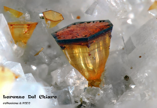
Wurtzite, Carrara Alpi apuane, photo by Lorenzo Del Chiaro
54 notes
·
View notes
Text

Updating the textbook on polarization in gallium nitride to optimize wide bandgap semiconductors
An updated model reconciles the gap between recent experiments and theory concerning polarization in wurtzite semiconductors—paving the way for the development of smaller, faster and more efficient electronic devices, according to a recent study by University of Michigan researchers.
The second most produced semiconductor behind silicon, gallium nitride is already widely used in LED lighting and high power, high frequency electronic devices. The material is expected to transform the next generation of cell phones and communications systems, and polarization underpins its stellar electronic performance.
"Gallium nitride semiconductors are already everywhere in our daily life and the impact is going to continue to grow," said Zetian Mi, a professor of electrical and computer engineering at U-M and senior author of the study published in Applied Physics Letters.
Read more.
#Materials Science#Science#Polarization#Gallium nitride#Semiconductors#Gallium#Nitrides#Wurtzite#University of Michigan
9 notes
·
View notes
Text
Wurtzite Structure
Introduction
The Wurtzite structure, named after the mineral Wurtzite, is a crystal structure common to many binary compounds. It represents a hexagonal close-packed array (hcp) and is a variant of the zinc blende structure. The structure is common to many semiconductors such as GaN, ZnS, and ZnO.
Basic Description of Wurtzite
The Wurtzite structure can be viewed as two interpenetrating…
View On WordPress
0 notes

Text
TF2 x SU AU
Posted it on Instagram and wanted to share here!
TF2 x SU AU doodles as my OCs!
AU made by the fabulous @lenny-link !!! ✨
In addition to background work because let’s be honest I need to draw backgrounds more….


Little gem info dump!
Wildcard (Wurtzite) used to work for Yellow Diamond as a solider, but because of his unstable gem condition it made him quite unpredictable. Resulting in shattering himself to able to go on his own.
Record (Scrapolite) works for Pink Dimond as a record keep and gem mercenary to find those that are no longer with the Diamonds. Currently on the search for the Yellow Pearl (Sniper).
#tf2 x su au#tf2 oc#tf2 ocs#steven universe#steven unvierse au#steven universe oc#background#background art#gem oc
69 notes
·
View notes
Text
Hardened hearts accept nothing from anyone. They push away anyone who attempts to get close to them, they do not want to be warmed with the flaming lies coming from untrue lips. They will not drop any wall that was built to keep away the unwavering aching. It is a far easier way to avoid the inevitable, gut-wrenching split of a heart that is far too fragile to be loved properly. Untrue lips will never have the opportunity to scar the vessel of one who has a wurtzite heart. This does not mean proper, veracious love is not craved. Many nights, I had fallen asleep, longing to be touched with the gentlest of hands, kisses trickling my shoulder blade until goosebumps rose on my hungry silhouette. I had always heard that love finds you when you aren't searching for it. I tried so many times to mold my mind into believing I wasn't searching for it. In reality, I looked everywhere for what I craved the most: to love and be loved. Until, one day, I decided I truly didn't want it. I was exhausted from taking the blows of what people claimed to be love. I wanted to live happily, without needing anyone, ever. Without half-truths, without explaining my choices, and without making the effort to understand another individual on a romantic level. It simply was not worth the pain caused by being loved improperly.
1 note
·
View note
Text

Fraunhofer IAF
Die verschiedenen Farbnuancen der AlYN/GaN-Wafer resultieren aus unterschiedlichen Yttrium-Konzentrationen sowie Wachstumsbedingungen.
Neues Halbleitermaterial AlYN verspricht energieeffizientere und leistungsfähigere Elektronik
Freiburg, 14.08.2024. Forschende des Fraunhofer IAF haben einen Durchbruch im Bereich der Halbleitermaterialien erzielt: Mit Aluminiumyttriumnitrid (AlYN) ist es ihnen gelungen, ein neues und vielversprechendes Halbleitermaterial mit dem MOCVD-Verfahren herzustellen und zu charakterisieren. Aufgrund seiner hervorragenden Materialeigenschaften und seiner Anpassungsfähigkeit an Galliumnitrid (GaN) besitzt AlYN ein enormes Potenzial für den Einsatz in energieeffizienter Hochfrequenz- und Hochleistungselektronik für Informations- und Kommunikationstechnologien.
Aufgrund seiner hervorragenden Materialeigenschaften hat Aluminiumyttriumnitrid (AlYN) das Interesse verschiedener Forschungsgruppen weltweit geweckt. Das Wachstum des Materials stellte bisher jedoch eine große Herausforderung dar. Bislang ist es nur gelungen, AlYN mit dem Magnetron-Sputter-Verfahren abzuscheiden.
Nun haben Forschende des Fraunhofer-Institut für Angewandte Festkörperphysik IAF es geschafft, das neue Material mithilfe der MOCVD-Technologie (metallorganische chemische Gasphasenabscheidung) herzustellen und damit die Erschließung neuer, vielfältiger Anwendungen zu ermöglichen.
»Unsere Forschung markiert einen Meilenstein in der Entwicklung neuer Halbleiterstrukturen. AlYN ist ein Material, das eine Leistungssteigerung bei gleichzeitiger Minimierung des Energieverbrauchs ermöglicht und damit den Weg für Innovationen in der Elektronik ebnen kann, die unsere digital vernetzte Gesellschaft und die stetig steigenden Anforderungen an Technologien dringend benötigen«, sagt Dr. Stefano Leone, Wissenschaftler am Fraunhofer IAF im Bereich Epitaxie.
Aufgrund seiner vielversprechenden Materialeigenschaften kann AlYN zu einem Schlüsselmaterial für zukünftige technologische Innovationen werden.
Jüngste Forschungen hatten bereits die Materialeigenschaften von AlYN wie Ferroelektrizität nachgewiesen. Die Forschenden am Fraunhofer IAF konzentrierten sich bei der Entwicklung des neuen Verbindungshalbleiters vor allem auf dessen Anpassungsfähigkeit an Galliumnitrid (GaN): Die Gitterstruktur von AlYN lässt sich optimal an GaN anpassen und die AlYN/GaN-Heterostruktur verspricht wesentliche Vorteile für die Entwicklung zukunftsweisender Elektronik.
Von der Schicht zur Heterostruktur
2023 hat die Forschungsgruppe am Fraunhofer IAF bereits bahnbrechende Ergebnisse erzielt, als es ihnen erstmals gelang, eine 600 nm dicke AlYN-Schicht abzuscheiden. Die Schicht mit Wurtzit-Struktur enthielt eine bis dato unerreichte Yttrium-Konzentration von über 30 Prozent. Nun haben die Forschenden einen weiteren Durchbruch erzielt: Sie haben AlYN/GaN-Heterostrukturen mit präzise einstellbarer Yttrium-Konzentration hergestellt, die sich durch hervorragende strukturelle Qualität und elektrische Eigenschaften auszeichnen. Die neuartigen Heterostrukturen verfügen über eine Yttrium-Konzentration von bis zu 16 Prozent. Unter der Leitung von Dr. Lutz Kirste führt die Gruppe für Strukturanalyse weitere detaillierte Analysen durch, um das Verständnis der strukturellen und chemischen Eigenschaften von AlYN zu vertiefen.
Die Fraunhofer-Forschenden konnten bereits äußerst vielversprechende und für den Einsatz in elektronischen Bauteilen interessante elektrische Eigenschaften von AlYN messen. »Wir konnten beeindruckende Werte für den Schichtwiderstand, die Elektronendichte und die Elektronenbeweglichkeit beobachten. Diese Ergebnisse haben uns das Potenzial von AlYN für die Hochfrequenz- und Hochleistungselektronik vor Augen geführt«, berichtet Leone.
AlYN/GaN-Heterostrukturen für Hochfrequenzanwendungen
Dank seiner Wurtzit-Kristallstruktur lässt sich AlYN bei geeigneter Zusammensetzung sehr gut an die Wurtzit-Struktur von Galliumnitrid anpassen. Eine AlYN/GaN-Heterostruktur verspricht die Entwicklung von Halbleiterbauelementen mit verbesserter Leistung und Zuverlässigkeit. Zudem besitzt AlYN die Fähigkeit zur Induktion eines zweidimensionalen Elektronengases (2DEG) in Heterostrukturen. Neueste Forschungsergebnisse des Fraunhofer IAF zeigen optimale 2DEG-Eigenschaften in AlYN/GaN-Heterostrukturen bei einer Yttrium-Konzentration von etwa 8 Prozent.
Die Ergebnisse aus der Materialcharakterisierung zeigen auch, dass AlYN in Transistoren mit hoher Elektronenbeweglichkeit (HEMTs) eingesetzt werden kann. Die Forschenden konnten einen signifikanten Anstieg der Elektronenbeweglichkeit bei niedrigen Temperaturen beobachten (mehr als 3000 cm²/Vs bei 7 K). Das Team hat bereits bedeutende Fortschritte bei der Demonstration der epitaktischen Heterostruktur erzielt, die für die Herstellung erforderlich ist, und erforscht den neuen Halbleiter weiter im Hinblick auf die Herstellung von HEMTs.
Auch für die industrielle Nutzung können die Forschenden eine positive Prognose wagen: Bei AlYN/GaN-Heterostrukturen, die auf 4-Zoll-SiC-Substraten gewachsen sind, konnten sie eine Skalierbarkeit und strukturelle Gleichmäßigkeit der Heterostrukturen demonstrieren. Die erfolgreiche Herstellung von AlYN-Schichten in einem kommerziellen MOCVD-Reaktor ermöglicht die Skalierung auf größere Substrate in größeren MOCVD-Reaktoren. Diese Methode gilt als die produktivste für die Herstellung großflächiger Halbleiterstrukturen und unterstreicht das Potenzial von AlYN für die Großserienfertigung von Halbleiterbauelementen.
Entwicklung von nichtflüchtigen Speichern
Aufgrund seiner ferroelektrischen Eigenschaften eignet sich AlYN in hohem Maße für die Entwicklung nichtflüchtiger Speicheranwendungen. Ein weiterer wichtiger Vorteil ist, dass das Material keine Begrenzung der Schichtdicke aufweist. Daher regt das Forschungsteam am Fraunhofer IAF an, die Eigenschaften von AlYN-Schichten für nichtflüchtige Speicher weiter zu erforschen, da AlYN-basierte Speicher nachhaltige und energieeffiziente Datenspeicherlösungen vorantreiben können. Dies ist besonders relevant für Rechenzentren, die zur Bewältigung des exponentiellen Anstiegs der Rechenkapazität für künstliche Intelligenz eingesetzt werden und einen deutlich höheren Energieverbrauch aufweisen.
Oxidation als Herausforderung
Eine wesentliche Hürde für die industrielle Nutzung von AlYN ist seine Oxidationsanfälligkeit, die die Eignung des Materials für bestimmte elektronische Anwendungen beeinträchtigen. »In Zukunft wird es wichtig sein, Strategien zur Minderung oder Überwindung der Oxidation zu erforschen. Dazu könnten die Entwicklung hochreiner Vorläuferstoffe, die Anwendung von Schutzbeschichtungen oder innovative Herstellungstechniken beitragen. Die Oxidationsanfälligkeit von AlYN stellt eine große Herausforderung für die Forschung dar, um sicherzustellen, dass die Forschungsanstrengungen auf die Bereiche mit den größten Erfolgsaussichten konzentriert werden«, folgert Leone.
Originalpublikation:
S. Leone et al. “Metal-Organic Chemical Vapor Deposition of Aluminum Yttrium Nitride”, Phys. Status Solidi RRL 17 2300091 (2023)
https://doi.org/10.1002/pssr.202300091
I. Streicher et al. “Two-dimensional electron gases in AlYN/GaN heterostructures grown by metal–organic chemical vapor deposition”, APL Materials 12 051109 (2024)
https://doi.org/10.1063/5.0203156
0 notes
Text
Various factors affecting the thermal conductivity of AlN ceramics
AlN is a covalently bonded compound with a stable structure and a hexagonal wurtzite structure without other isomorphs. Its crystal structure is composed of AlN4 tetrahedrons generated by the dislocation of aluminum atoms and adjacent nitrogen atoms as structural units and belongs to the hexagonal crystal system.
The main characteristics of AlN ceramics:
(1) High thermal conductivity, 5-10 times that of alumina ceramics;
(2) The thermal expansion coefficient (4.3×10⁻⁶/℃) matches that of semiconductor silicon materials (3.5-4.0×10⁻⁶/℃);
(3) Good mechanical properties;
(4) Excellent electrical properties, with extremely high insulation resistance and low dielectric loss;
(5) Multi-layer wiring can be performed to achieve high density and miniaturization of packaging;
(6) Non-toxic and environmentally friendly.
The following are the factors that affect the thermal conductivity of AlN ceramics.
At 300K, the theoretical thermal conductivity of AlN single crystal material is as high as 319W/(m·K). However, in the actual production process, due to the influence of various factors such as material purity, internal defects (dislocations, pores, impurities, lattice distortion), grain orientation, and sintering process, its thermal conductivity will also be affected and is often lower than the theoretical value.

Effect of microstructure on thermal conductivity
The heat conduction mechanism of single crystal AlN is phonon heat transfer, so the thermal conductivity of AlN may be mainly affected by the grain boundaries, interfaces, second phases, defects, electrons, and phonons in the crystal. From the perspective of microstructure, the interaction between phonons, the interaction between phonons and impurities, and the grain boundary defects will all cause scattering, which will affect the mean free path of phonons and thus affect its thermal conductivity.
The microstructure of AlN has a great influence on its thermal conductivity. If you want to obtain aluminum nitride ceramics with high thermal conductivity, try to make the aluminum nitride crystals have fewer defects and less impurities.
Effect of oxygen impurity content on thermal conductivity
Studies have shown that AlN has a strong affinity with oxygen and is easy to oxidize, resulting in the formation of aluminum oxide film on its surface. Due to the dissolution of oxygen atoms in Al2O3, the position of nitrogen atoms in AlN is replaced, aluminum vacancies are generated, and oxygen defects are formed. The aluminum vacancies formed scatter phonons, resulting in a decrease in the mean free path of phonons, so the thermal conductivity of the AlN substrate will also decrease.
The study concluded that the types of defects in the AlN lattice are related to the concentration of oxygen atoms.
● When the oxygen concentration is lower than 0.75%, oxygen atoms are evenly distributed in the AlN lattice, replacing the position of nitrogen atoms in AlN, and aluminum vacancies are generated;
● When the oxygen concentration is not lower than 0.75%, the position of aluminum atoms in the AlN lattice will change, aluminum vacancies disappear, and octahedral defects will be generated;
● When the concentration of oxygen atoms is higher, its lattice will produce polymorphs, inversion domains, oxygen-containing stacking faults, and other ductile defects. Taking thermodynamics as the starting point, the study found that the amount of oxygen in the aluminum nitride lattice is affected by the Gibbs free energy of the aluminate reaction |ΔG°|. The larger |ΔG°| is, the less oxygen is in the AlN lattice, and thus the thermal conductivity will be higher.
It can be seen that the thermal conductivity of AlN is seriously affected by oxygen impurities, and the presence of oxygen impurities is an important reason for the reduction of its thermal conductivity.
Appropriate sintering aids can improve thermal conductivity
To improve the thermal rate of AlN, it is usually chosen to add the required sintering aids during sintering to reduce the sintering temperature, remove oxygen in the lattice, and thus improve the thermal conductivity of AlN.
At present, the addition of multi-component composite sintering aids is of great concern. Experiments have found that when composite sintering aids Y2O3-Li2O, Y2O3-CaC2, Y2O3-CaF2, and Y2O3-Dy2O3 are added to AlN, a denser AlN sample with less oxygen impurities and second phases can be obtained.
Choosing a suitable composite system of sintering aids can achieve a lower sintering temperature of AlN effectively purify the grain boundaries, and obtain AlN with higher thermal conductivity.
0 notes
Text
The present study aimed to investigate the structural, morphological, elemental, optical properties and photocatalytic activity of the bare zinc oxide (ZnO) and Manganese-doped zinc oxide (Mn- ZnO) nanoparticles (NPs) using terasil blue (TB) dye as a model substrate.
Materials and Methods: The ZnO and Mn-doped ZnO catalysts were synthesized using the co-precipitation method. The synthesized photocatalysts were characterized by X-ray diffraction (XRD), energy dispersive X-ray (EDX), and scanning electron microscopy (SEM). The band energies were measured using ultraviolet-visible (UV-Vis) spectrophotometry.
Results: The results obtained from XRD, EDX, SEM, and UV-Vis analyses demonstrated a successful synthesis of bare and Mn-doped ZnO nanoparticles. The diffraction patterns for the synthesized ZnO and Mn-doped ZnO photocatalyts were matched with that of the standard hexagonal wurtzite structure of the standard ZnO catalyst. The average particle size for the ZnO and Mn-doped ZnO catalysts were found to be 23.46 nm and 24.38 nm, and band gap energies of 3.28eV and 3.09eV, respectively. The photocatalytic performance of the Mn-doped ZnO photocatalyst was optimized using box behnken design of response surface methodology under visible light irradiation. The operational parameters involved TB initial concentration, catalyst dosage, initial pH, and irradiation time. The optimum photodegradation efficiency of TB dye removal was achieved at 96.75% of 15mg/L of TB concentration, 0.1g/L of Mn-doped ZnO, pH = 10, and 160 minutes of irradiation time. Moreover, the photocatalytic degradation of TB over the Mn-doped ZnO nanoparticles followed the pseudo-first-order kinetics model (k = 0.0254 min-1).
Conclusion: Finally, the evaluation of various scavengers confirmed that the photogenerated holes and hydroxyl radicals were the major radicals for the TB photodegradation over the Mn-doped ZnO nanoparticle under visible light irradiation.
instagram
0 notes
Text
0 notes
Text
When we communicate with others over wireless networks, information is sent to data centers where it is collected, stored, processed, and distributed. As computational energy usage continues to grow, it is on pace to potentially become the leading source of energy consumption in this century. Memory and logic are physically separated in most modern computers, and therefore the interaction between these two components is very energy intensive in accessing, manipulating, and re-storing data. A team of researchers from Carnegie Mellon University and Penn State University is exploring materials that could possibly lead to the integration of the memory directly on top of the transistor. By changing the architecture of the microcircuit, processors could be much more efficient and consume less energy. In addition to creating proximity between these components, the nonvolatile materials studied have the potential to eliminate the need for computer memory systems to be refreshed regularly.
Their recent work published in Science explores materials that are ferroelectric, or have a spontaneous electric polarization that can be reversed by the application of an external electric field. Recently discovered wurtzite ferroelectrics, which are mainly composed of materials that are already incorporated in semiconductor technology for integrated circuits, allow for the integration of new power-efficient devices for applications such as non-volatile memory, electro-optics, and energy harvesting. One of the biggest challenges of wurtzite ferroelectrics is that the gap between the electric fields required for operation and the breakdown field is very small.
Read more.
#Materials Science#Science#Data storage#Electronics#Computing#Ferroelectric#Wurtzite#Carnegie Mellon#Penn State
10 notes
·
View notes
Text
əbdtgəæpdrətrbəellun
Pronounced: uhbdtguhapdruhtrbuhellun.
Pantheon of: substantiality, human nature, duality, individuality, impracticability, compulsiveness, seriousness.
Entities
Mnɑərʃiaɪðəmɛsnæɛʒənz
Pronounced: mnahuhrshiaithuhmaysnaayzuhnz
Seriousness: sedateness.
Impracticability: infeasibility.
Compulsiveness: workaholism.
Individuality: peculiarity.
Prophecies: electrification, runup, restriction.
Relations: nnəəwtɑsbtɒhəɪærsmʌr (corundom).
Nnəəwtɑsbtɒhəɪærsmʌr
Pronounced: nnuhuhwtahsbtouhuhiarsmur
Seriousness: committedness.
Impracticability: infeasibility.
Compulsiveness: workaholism.
Individuality: peculiarity.
Legends: reform, case study.
Prophecies: open primary.
Relations: rktvɪtikrtrðɑəkbŋægi (frequency), mnɑərʃiaɪðəmɛsnæɛʒənz (siderite), əsʃəsɑltnislvirɛkkɪr (coca cola), əʃklvraɪəɑrpərəstɛzin (eponym).
Rktvɪtikrtrðɑəkbŋægi
Pronounced: rktvitikrtrthahuhkbngagi
Seriousness: graveness.
Impracticability: infeasibility.
Compulsiveness: obsessiveness.
Individuality: singularity.
Legends: carol.
Tktrnkɪɪnkɪmrwvʃiəoæ
Pronounced: tktrnkiinkimrwvshiuhoa
Seriousness: sedateness.
Impracticability: infeasibility.
Compulsiveness: obsessiveness.
Individuality: peculiarity.
Legends: imitative electronic deception, wake.
Prophecies: carrot.
Relations: mnɑərʃiaɪðəmɛsnæɛʒənz (benefit), əsʃəsɑltnislvirɛkkɪr (zanzibar copal), əʃklvraɪəɑrpərəstɛzin (endorphin).
Əsʃəsɑltnislvirɛkkɪr
Pronounced: uhsshuhsahltnislviraykkir
Seriousness: committedness.
Impracticability: infeasibility.
Compulsiveness: workaholism.
Individuality: singularity.
Prophecies: oil change, hostilities.
Relations: mnɑərʃiaɪðəmɛsnæɛʒənz (raw umber), rktvɪtikrtrðɑəkbŋægi (calcium carbide), nnəəwtɑsbtɒhəɪærsmʌr (histidine), əʃklvraɪəɑrpərəstɛzin (wurtzite).
Əʃklvraɪəɑrpərəstɛzin
Pronounced: uhshklvraiuhahrpuhruhstayzin
Seriousness: graveness.
Impracticability: infeasibility.
Compulsiveness: obsessiveness.
Individuality: peculiarity.
Legends: mudra.
Prophecies: combination, deal.
Relations: tktrnkɪɪnkɪmrwvʃiəoæ (hidden reserve), əsʃəsɑltnislvirɛkkɪr (hemiacetal), rktvɪtikrtrðɑəkbŋægi (acetic acid).
0 notes
Text
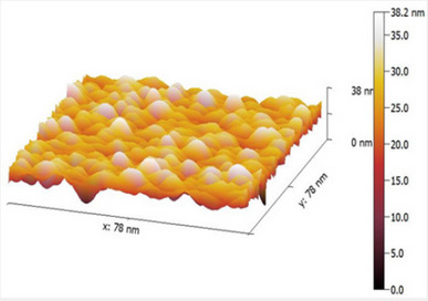
The Morphological Properties of Zns Nanoparticles Deposited on Glass Substrates as a Function of Aluminum Content
Authored by: A A Ahmed
Abstract
The pulsed-laser deposition (PLD) method was used to deposit undoped zinc sulphide (ZnS) and Al-doped zinc sulphide (AZS) films on glass substrates (GSs). The aluminum content in the ZnS films varied from 0% to 8%. The film morphology was studied using atomic force microscopy (AFM). The films were optically characterized using an Ultraviolet–Visible-near-infrared (UV-VIS-NIR) spectrophotometer with photon wavelengths ranging from 300 to 600nm. The average roughness (Sa), root-mean square (RMS) roughness (Sq), surface skewness (Ssk), and surface kurtosis (Suk) parameters of the samples were determined using the AFM method. The samples’ AFM grain sizes were found to be 4.89 nm, 5.65 nm, and 12 nm, respectively. The doped ZnS thin film’s surface roughness was found to be greater than the undoped ZnS thin film’s. The samples showed a high transmittance across the whole visible spectrum, according to the UV data. The film optical refractive-index (n) and the extinction-coefficient (k) was computed using UV–VIS spectroscopy data. The techniques used in these investigations have been described and explained in detail. Good agreement was found when comparing results from this work against previously published data.
Keywords: Thin film; PLD; AFM; UV; Surface roughness
Abbreviations: The Pulsed-Laser Deposition; AZS: Al-Doped Zinc Sulphide, GSs: Glass Substrates; AFM: Atomic Force Microscopy; UV-VIS-NIR: Ultraviolet–Visible-Near-Infrared; RMS: Root-Mean Square; Ssk: Surface Skewness; Suk: Surface Kurtosis
Introduction
The metal chalcogenide in their crystalline state possesses many outstanding properties and has attracted considerable attention in the literature [1]. Semiconductor nanoparticles (SCNPs) films made of II-VI compounds have distinct properties that make them suited to several devices and applications [2]. Tin dioxide (SnO2), titanium-dioxide (TiO2), cadmium-sulphide (CdS), cadmium-tellurium (CdTe), cadmium-selenide (CdSe), zinc selenide (ZnSe), zinc-oxide (ZnO), and zinc tellurium (ZnTe) are all well-known SCNPs and well-studied in detail [3-10]. Among the SCNPs, ZnS is one in particular that has been widely used for a variety of applications. ZnS is an easily accessible, nontoxic, and environmentally safe compound with a higher direct band-gap energy (3.7 eV) [11].
ZnS is a metal chalcogenide with a high refractive index, a large band-gap energy, and a high UV-visible transmittance [12,13]. The polytypes of ZnS are cubic-zinc blende (sphalerite) and wurtzite (hexagonal) [11]. Furthermore, ZnS structures frequently crystallize in space groups (F43m) and (P63) in the cubic zincblende (ZB) phase at low temperatures, and (P63) in the hexagonal zincblende (ZB) phase at high temperatures [11]. Several research groups have attempted to dope ZnS films with elements such as In, Al, Fe, Co, Pb, Cd, Cu, Mn, Cr, Ni, Eu, Sm, and Cl throughout the growth process [14-20]. However, there have been infrequent studies on aluminum doped with ZnS films and placed on substrates [21,22]. However, aluminum doped ZnS films deposited on glass needs further investigation. Numerous deposition techniques, including sputtering, thermal evaporation, spray pyrolysis, chemical bath deposition, close-spaced evaporation, electron beam evaporation and pulsed laser deposition have been used to prepare ZnS thin films [14,23-26].
To our knowledge, only a few investigations was conducted on zinc sulphide thin films prepared via the PLD method on glass substrates. Several methods are demonstrated, but the pulsed laser deposition technique is shown to maintain the desired composition in the deposited thin films. Because the high kinetic energy of atoms and ionized particles in the laser-produced plasma, the PLD method can be used to deposit ZnS film at low temperatures [27]. This method is used to deposit materials on large surfaces under air conditions and on a variety of substrates in a well-controlled manner. Nonetheless, due to the intricate growth mechanism and method, deposition of ultrathin ZnS and AZS films via PLD remains extremely challenging. The results of these analyses, performed by utilizing the AFM method and the UV–Vis spectroscopy, have been documented.
Materials and Methods
Sample preparation
Sigma-Aldrich analytical grade reagents, chemical, and sodalime glass substrates were purchased and used without further purification in this investigation. The precursors for Al, S, and Zn were aluminum chloride hexahydrate (AlCl3.6H2O), thioacetamide (CH3CSNH2), zinc acetate dehydrate [Zn(CH3COO)2, 2H2O)], and ethylenediamine (NH2CH2CH2NH2) of analytical reagent quality. For several minutes, the zinc-acetate and ethylenediamine were mixed and agitated to obtain a clear and uniform solution. The product was then added to the zinc-acetate solution, followed by the addition of tri-sodium citrate. The resulting solution was agitated for a few minutes in each case. Following this, it was added to the previously produced thiourea solution while stirring. To obtain Al-doped ZnS (AZS) samples, the combined materials were mixed in the proper ratio and then dried. Numerous hours were spent extensively rushing the combined AZS samples. To manufacture the pellets of the thin films, a 5-ton hydraulic press was used for 3-5 minutes at room temperature.
Thus, pellets roughly 1.2cm in diameter and 0.2cm thick were produced from the given AZS sample. The glass substrates were degreased for 12 hours prior to deposition using soap water and alcohol. Following this procedure, glass substrates (GSs) were ultrasonically cleaned for 10 minutes with alcohol and deionized water. Finally, the glass slide substrate was rinsed, washed with deionized water, and air dried. PLD with a focused Q-switchedneodymium- doped yttrium aluminum garnet (Nd: Y3Al5O12) was used to deposit the ZnS and AZS films on the glass substrates (GSs) (Nd: YAG). The depositions took place at four-hour intervals.
Pulsed-laser ablation was carried out using a focused beam in TEM00 mode laser with primary and secondary harmonic outputs at 1064 and 532nm, respectively. The laser system was operated using pulses with a duration of ten nanoseconds. A pulsed laser with an energy density of 2 J/cm2 and a frequency of 6 Hz was used to irradiate the object. The thin film target spun as the laser restored across an area of approximately 0.5cm2 with a spot size of 3 mm2 and an incidence angle of 45°.
Throughout the development process, the target-substrate distance was maintained at a constant of 2.0cm. The substrate was clamped to a heated holder, and the temperature of the deposition solution was measured. Prior to heating the source, the chamber was evacuated to a pressure of 10-3 torr. The ZnS and AZS film were deposited on the GSs using 500 pulses and 100 mJ/pulse energy. The target and laser source were separated by a predetermined distance of 12.0cm. All films were of a thickness of between 200 and 250nm. However, when the films were grown using the PLD method, the deposition rate was calibrated, in order to regulate the thickness. The details concerning the set-up of the PLD method experiment have been provided elsewhere [14]. All samples were labeled as a control (ZnS/GSs or S0), the Al-doped ZnS/GSs (ZnS/ GSs: Al 4% or S1) and the (ZnS/GSs: Al 4% or S2), respectively. The sample morphology and optical properties were measured by the AFM [28] and the UV–Vis spectrophotometer [29].
Results and Discussion
The surface roughness of the films, as defined by arithmeticmean height (Sa), root-mean square height (Sq), skew (Ssk), and kurtosis (Sku), was measured and is shown in table 1. The film arithmetic mean height was calculated to be S0 (5.509nm), S1 (9.964nm), and S2 (23.92nm), in that order. It was observed that in comparison to S0, the Sa of the sample surface increased from 5.509nm to 23.92nm with aluminum doping. The film root-mean square roughness was calculated to be S0 (7.251nm), S1 (13.30 nm), and S2 (44.11nm), in that order.
The sample skewness was found to be S0 (0.7310), S1 (1.179), and S2 (3.585), respectively. The sample kurtosis was S0 (5.046), S1 (10.38), and S2 (20.36), respectively. These findings show that the doped sample surface of S1 and S2 was rougher than the S0 surface. The dopant of ZnS/glass substrates led to a slight alteration of the parameters. However, the Sa and Sq film parameters had increased. Furthermore, the Ssk and Sku parameters of the film increased from 0.7310 to 3.585, and from 5.046 to 20.36, respectively.
AFM micrographs of the prepared films show that spherical shape grains are uniformly distributed. Surface kurtosis values greater than 3 were found in all the examined samples, indicating sharper peaks and longer, fatter tails in general. Rku values greater than 3 indicate that the peaks and valleys have further flattened out. This finding suggests that Rsk can be used to distinguish the roughness profiles of the two surface processes. Surface roughness analysis was performed by capturing 3-D images of the surfaces of ZnS thin films with a scan area of 7.8nm x 7.8nm.
Figure 1 depicts the 7.8nm x 7.8nm 3-D images of the undoped and doped ZnS thin film surfaces for (a), (b), and (c), respectively. It is observed that Al doping induced noticeable changes in the surface morphology. The size of the grains increased for 4 wt. % Al doping (Figure 1(b)), and bigger clusters were formed on the film surface for 8 wt. % a Al doping, as shown in figure 1(c). It was also reported that Al doping in ZnS led to an increase in the grain growth.
The scales of the Z-axis in figures 1a-1c show that the surface of the undoped deposited ZnS thin film is much flatter, in comparison with the surface of the doped deposited ZnS thin film (c). When the aluminum content is gradually increased, the scales of the Z-axis of the undoped deposited ZnS thin film surface increases. It is seen in figures 1a-1c that the scales of the Z-axis are different. Figure 2 depicts a histogram of the percentages of ZnS and ZnS: Al as a function of grain size (a to c). The AFM analysis extracts surface parameters from the AZS thin films, allowing for the investigation of the surface analysis with numerical data.
The profiles of the AFM image cross section are shown in figure 2. The AFM image cross-section shows that islands in samples grown with aluminum concentrations of 0%, 4%, and 8% have a quasi-rounded shape distribution with an RMS value of 4.89nm and 5.65nm, for 0% and 4%, respectively. In contrast, for an aluminum concentration of 8%, the profiles exhibit a quasitriangular distribution of islands with an RMS value of 12nm.
The origin of the rough surface morphologies is correlated to the enhanced aluminum at a high aluminum concentration of 8%. Small ZnS islands tend to coalesce into larger ones as a result of the extra aluminum migrating on the surface. This coalescence allows for a reduction in the density of ZnS islands. Thus, 0% aluminum concentrations favor the 2D-like growth of ZnS, resulting in a wavy surface.
A quantitative optical model was employed in the calculation of the concentration-dependent reflectance of AZS structures, as detailed below. The experimental results add to our understanding of the relationship between aluminum concentrations and optical properties. A UV–Vis–NIR spectrophotometer in the 600 nm range was used to measure the optical properties of AZS thin films at room temperature. The reflectance spectrum was obtained using a UV–Vis–NIR spectrophotometer. The effects of variables on roughness were investigated using both morphological and optical responses. Table 2 shows a more detailed comparison of the films’ refractive index (n), extinction coefficient (k), reflectance (R), and surface roughness (Sa). However, as the refractive index, extinction coefficient, and reflectance of a material decrease, the value of its surface roughness increases.
In summary, we provide a correlation between Aluminum concentration and surface morphology evolutions versus the optical parameters of AZS on substrate based on the optical properties results. The results show that the high-density island structure acts to increase the scattering of the AZS surface. Changing the concentration of Al can affect the density and size of islands.
We compare the surface roughness, aluminum content, and reflectance as shown in figure 3. It is significant to note that the contribution of all surface defects and features is regarded as the primary cause of light scattering, as a result of which reflectance decreases for reflectance measurements. Finally, based on the reflectance data, we present a correlation between AZS concentration and surface morphology.
Conclusion
In summary, un-doped and Al-doped ZnS film was deposited on glass substrates using the PLD technique. The effects of aluminum concentration on the morphological and optical properties of the films were investigated using AFM and UV methods. According to the AFM studies, the film roughness changed significantly, following dopant treatment. The average roughness, rootmean square roughness, line skewness, and kurtosis of the ZnS films deposited on the glass substrates slightly increased after aluminum content-treatment. The AFM topography of doped and deposited films with aluminum content ranging from 0% to 4% revealed a surface texture with waviness.
To Know More About Juniper Online Journal Material Science Please click on:
https://juniperpublishers.com/jojms/index.php
For more Open Access Journals in Juniper Publishers please click on:
https://juniperpublishers.com/index.php
#Juniper Publishers#Material Science#Materials Theory#Structural Materials#Juniper publisher reviews#Juniper publisher journals
1 note
·
View note
Text
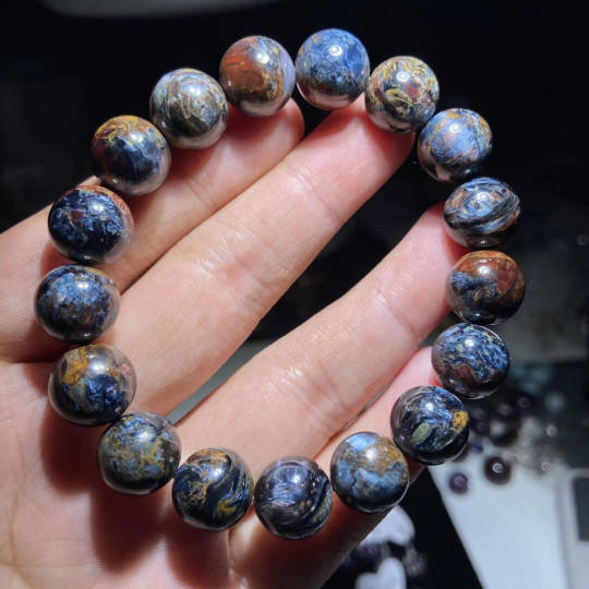
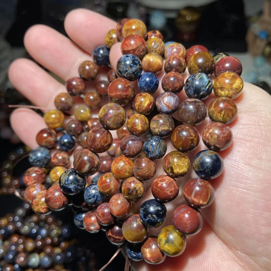
Main Components and Morphological Characteristics of Pietersite
The main components of Pietersite:
The original mineral components are mainly alkaline and alkaline earth amphibole asbestos, including magnesium sodium amphibole asbestos, calcium magnesium sodium amphibole asbestos, sodium aluminum actinolite asbestos, tremolite asbestos, sodium actinolite asbestos and actinolite asbestos.
The main mineral compositions are: chalcedony, quartz, sometimes associated red, white agate and onyx, opal, trace specularite, pyrite, hematite (limonite), albite, calcite, barite, and wurtzite. The chalcedony is a colorless cryptocrystalline aggregate with greasy luster. From the appearance, the chalcedony tends to bond or wrap blue asbestos after the formation of blue asbestos, making it a colorful tiger eye mineral. The presence of iron oxide makes Pietersite show different colors. Blue asbestos fiber, which is not weathered or iron stained, is blue; Those that have been mineralized by ferritization are purplish red; The weathered ones are golden yellow. The minerals in the blue asbestos veins show obvious zoning and other functions.
Morphological characteristics of Pietersite:
The products developed by pietersite are all inclusive. If you watch this product in detail, you will be happy to forget about the world of strange magic colors. For example, the scenic brand can be said to be the living color of the earth's activities and changes over thousands of years. There are spectacular scenes of volcanic eruptions, as well as flowing magma flashing red, yellow and gold; It also seems that there are various natural materialized art color changing patterns, which are very beautiful. Pietersite symbolizes safety. The jewelry produced has the effect of cat's eye (moving light and shadow), and also looks like the bright eyes of a tiger. Because of its majestic spirituality, it is sacred and inviolable, and is considered to be a gem for eliminating disasters and evil spirits, and for attracting good luck. Wearing gems can improve decision and creativity. It is inspiring to make progress.
Like opal, it has obvious and unique features, like stern eyes, more like mysterious boundaries. From different angles, it differs from opal in that the color of Peter's cat's eyes is more domineering and gorgeous.
Since ancient times, it has always been a gem that people yearn for and want to own.
In this ore group, a series of colorful ore bodies have been formed due to different growth environments and trace elements. The common ore is brown yellow, while the blue gray and red brown are few. Among them, the ones with clear, bright and complete eyeliner, good gloss and clear grain, no impurities on the stone, uniform texture and best color. It is considered as a treasure of nature and a miracle of the earth. The unique gem structure is like the eyes of an elf, flickering, mysterious and colorful, full of spirituality, and represents the life endowed by nature.

0 notes
Text
Disk led free

DISK LED FREE FREE
We derive the effective-mass Hamiltonian for wurtzite semiconductors, including the strain effects. This strain confinement mechanism is the origin of the luminescence quenching in very thin GaN quantum disks, as well as the main source of the emission linewidth broadening. This strain reduction annihilates partially the piezoelectric field, giving rise to a specific carrier confinement mechanism (strain confinement), that depends on the disk thickness.
DISK LED FREE FREE
An inhomogeneous biaxial (in-plane) strain distribution within the GaN quantum disks, pseudomorphically grown on strain-free AlxGa1-xN nanocolumns, results from a reduction of the accumulated elastic energy at the disk free surface (GaN-air boundary). Experimental emission energies are compared to theoretical calculations based on a one-dimensional Schrödinger-Poisson solver, including spontaneous and piezoelectric polarizations, surface potentials, and strain. This paper will show that NIL is an excellent technology to produce nanopatterned GaN substrates highly suitable to grow defect free arrays of positioncontrolled nanorods for ultrahigh brightness LED applications.Ĭarrier confinement effects in nanocolumnar AlxGa1-xN/GaN multiple quantum disks have been studied by photoluminescence, as a function of the Al content and quantum disk thickness. The nanopatterns created by NIL can be applied to control metal organic vapour phase epitaxy (MOVPE) growth of GaN nanorods. The mentioned irregularities are particularly disturbing when NIL based processes are utilized to create patterns onto the wafer surface. These types of substrates suffer from growth defects like hexagonal spikes, vpits, waferbowing, atomic steps and surface corrugations on a scale of few 10 mum or even large islands of irregularities. The wafers used for producing LED's are typically III/V semiconductor materials grown with epitaxial processes. One of the first application areas in which NIL is used is manufacturing of various types of LED's. Nano Imprint Lithography (NIL) is a promising technology that combines low costs with high throughput for fabrication of sub 100 nm scale features.
0 notes
Text
Performance characteristics of aluminum nitride materials
Aluminum nitride (AlN) has the characteristics of high strength, high volume resistivity, high insulation withstand voltage, thermal expansion coefficient, and good matching with silicon. It is not only used as a sintering aid or reinforcing phase for structural ceramics, especially in recent years. In the field of ceramic electronic substrates and packaging materials, its performance far exceeds that of alumina.
Aluminum nitride materials have broad application prospects and a wide range of potential markets in the electronic field and electric power, locomotives, aviation and aerospace, national defense and military industry, communications, and many industrial fields. Higher-end applications have become a hot topic with the development of aluminum nitride crystal materials. Among them, the application of aluminum nitride in the semiconductor field has always attracted much attention.
Aluminum nitride (AlN) is a covalently bonded compound with a hexagonal wurtzite structure, with lattice parameters a=3.114 and c=4.986. Pure aluminum nitride is blue-white, and AlN usually appears gray or off-white under normal conditions. As a material with great potential, aluminum nitride has these performance characteristics:
Thermal properties
The theoretical thermal conductivity of AlN is 320W/m·K. The thermal conductivity of actually prepared polycrystalline AlN is generally 100~260W/m·K. The room temperature thermal conductivity is 10~15 times that of Al2O3, close to BeO ( The theoretical thermal conductivity is 350W/m·K), and when the temperature is higher than 200°C, the thermal conductivity is better than beryllium oxide; in the range of 25~400°C, the thermal expansion coefficient of pure AIN is 4.4×10⁻⁶K- 1, which is similar to the thermal expansion coefficient of silicon (3.4×10⁻⁶K-1).
Electrical properties
The room temperature cathode conductivity of pure AIN is greater than 1014Ω·cm, which is a good insulating material; the dielectric constant is about 8.0 (1MHz), which is equivalent to Al2O3; the dielectric loss is 10-4 (1MHz), and the insulation withstand voltage is 14KV ·mm-1, high electromechanical coupling coefficient (0.8%), piezoelectricity and pro-negative productivity.
Mechanical properties
At room temperature, the dense AIN ceramic has a Vickers hardness of 12GPa, a Mohs hardness of 7~8, a Young's modulus of 308GPa, and a flexural strength of up to 350MPa. The strength decreases slowly as the temperature rises. The high-temperature strength ratio at 1300°C The room temperature strength is reduced by about 20%, while the hot-pressed Si3N4 and Al2O3 are generally reduced by 50%.
chemical properties
AIN has excellent high-temperature corrosion resistance, is not wetted by aluminum, copper, silver, lead, nickel, and other metals, and can also exist stably in certain molten salts such as gallium arsenide; AIN has strong hygroscopicity It is highly reactive and easily reacts with water vapor in the air; in the air, the initial oxidation temperature of AIN is 700~800°C. Under normal pressure, AIN will not melt, but will thermally decompose at 2260-2500°C.
0 notes
Last Seen Blogs

ren-needsaving
moonchild🌙

metartnetwork
MetArt™ Network

silverkeysmtl
Silverkeys

ragingmusclesexual
MuscleSexual MuscleSlut

qibsichan
🌙Smaller Bodies Initiative☀️