#Automatic PCB Assemble Factory
Explore tagged Tumblr posts
Visit Tumblr Blog
Explore Tumblr blogs with no restrictions, modern design and the best experience.
Last Seen Tumblr Blogs


Fun Fact
There were a total of 171.5 billion posts on Tumblr in 2019.
Text
Top Trends in PCB Assembly for 2025
PCBs are the heart of the modern world. Whether it’s household equipment, industrial equipment, or defense ordnance, printed circuit boards are running everything. With new developments, the global scene of PCB manufacturing is changing rapidly. Using the newest technologies is not only a great concept, but staying competitive depends on it as well. From downsizing to AI-driven manufacturing, 2025 promises to bring major breakthroughs along with making advancements in current technologies that will change the way Printed Circuit Boards (PCBs) are manufactured.
This article will walk you through some key industry trends that will sketch the future of PCB assembly.
5 Key Trends in PCB Assembly to Follow in 2025
As the world is moving towards manufacturing more complex products and adopting advanced technologies, the PCB assembly industry is also observing several key trends. Here are a few noteworthy trends to follow.
1. Shrinking is in High-Density Interconnections: HDI and Miniaturization
Think about our daily gadgets, such as wearables, Internet of Things devices, and sophisticated medical electronics. These devices need robust and small PCBs, and therefore, in these spaces, High-Density Interconnect (HDI) technology excels. HDI lets electronic gadgets be more powerful despite their compact stature. In what manner? For high-speed applications, it increases signal integrity, lowers component spacing, and permits smaller trace lengths, hence enhancing electrical performance. And it will change the entire PCB manufacturing market.
According to a forecast [1], the HDI PCB market is expected to rise rapidly and, by 2032, will reach almost $40 billion. That makes the direction in which things are heading quite obvious.
2. Smart Factories: Artificial Intelligence and Automation
Like in every other industry, PCB assembly is becoming significantly faster, smarter, and more efficient. Industry 4.0 and manufacturing driven by artificial intelligence lead the push. Think about robotic soldering and pick-and-place robots for fast, more perfect component installation. Artificial intelligence and machine learning have found their way into quality control, that is, for error reduction and flaw detection done automatically. Imagine the Internet of Things, connected production lines, allowing real-time monitoring and predictive maintenance.
3. Bendable and Adaptable: Rigid-flexible PCBs
Flexible and rigid-flex printed circuit boards are becoming more popular in industries such as transportation, aircraft, and healthcare electronics. But you may think, why so? Because of their small size and lightweight nature, they are ideal for manufacturing small, portable electronic devices. They can withstand significant external force and resist bending and vibration. They endure longer with fewer interconnect failures, making them more reliable.
4. Green is Good: Manufacturing Sustainable Circuit Boards
Growing worries about e-waste and carbon footprints force sustainability to the front stage in PCB production. Lead-free soldering, biodegradable and reusable substrates, recyclable materials, and energy-efficient manufacturing procedures will become the focal points in the near future. It’s about matching global laws and customer demand as much as it is about environmental responsibility.
5. Printing the Future: 3D Printing in PCB Assembly
Additive manufacturing is revolutionizing PCB manufacturing and streamlining complex multilayer design construction. From this, faster prototyping, reduced material waste, and more customization for specific uses follow. This is a breakthrough for design and development; it will only get more so.
The Final Thought
There are a lot of exciting new possibilities in the PCB assemblyand PCB manufacturing industries. Miniaturization, automation, sustainability, and developments in AI-driven manufacturing will enable you to produce premium printed circuit boards (PCRs) that satisfy future electronics needs. Survival in a dynamic industry depends on keeping ahead of the competitors. By following these trends and wise technology investments, you could set yourself up for success in 2025 and beyond.
Know More : https://www.pcbpower.us/blog/top-trends-pcb-assembly
0 notes
Text
The Essential Guide to SMT Equipment in Modern Electronics Manufacturing

Introduction to SMT Equipment
SMT equipment (Surface Mount Technology equipment) is the backbone of modern electronics manufacturing. As consumer and industrial electronics continue to shrink in size while increasing in complexity, the demand for efficient and precise SMT machinery has grown exponentially. This guide explores the different types of SMT equipment, their functions, and their importance in producing high-quality printed circuit boards (PCBs).
Key Components of SMT Equipment
1. Solder Paste Printing Machines
The first step in the SMT assembly process is applying solder paste to the PCB. Solder paste printers use stencils to deposit precise amounts of solder paste onto the board’s pads. Advanced models feature:
Vision alignment systems for high accuracy
Automatic stencil cleaning to prevent clogging
Real-time inspection to detect printing defects
2. Pick-and-Place Machines
Pick-and-place machines are the most critical SMT equipment in the production line. They accurately place surface-mount components (SMDs) onto the PCB at high speeds. Modern pick-and-place machines offer:
High-speed placement (up to 100,000 components per hour)
Multi-nozzle systems for handling different component sizes
Machine vision systems for precision alignment
3. Reflow Ovens
After component placement, the PCB moves through a reflow oven, where the solder paste melts and forms strong electrical connections. Key features include:
Multiple heating zones for controlled temperature profiles
Nitrogen gas environments to reduce oxidation
Cooling systems to solidify solder joints quickly
4. Inspection and Testing Equipment
Quality control is crucial in SMT manufacturing, and inspection systems ensure defect-free production. Common SMT inspection tools include:
Automated Optical Inspection (AOI) – Detects misaligned or missing components
X-ray Inspection (AXI) – Examines hidden solder joints (e.g., under BGA components)
In-Circuit Testing (ICT) – Verifies electrical functionality
Advancements in SMT Equipment Technology
1. Automation and Industry 4.0 Integration
Modern SMT machines increasingly incorporate IoT (Internet of Things) and AI-driven analytics. Smart factories use real-time data to:
Optimize machine performance
Predict maintenance needs
Reduce downtime
2. Miniaturization and High-Density Assembly
As components shrink (e.g., 01005 resistors, ultra-fine-pitch ICs), SMT equipment must adapt with:
Higher placement accuracy (micrometer-level precision)
Advanced feeders for tiny components
Laser-assisted alignment for micro-BGA and QFN packages
3. Eco-Friendly SMT Solutions
Sustainability is becoming a priority in electronics manufacturing. New SMT machinery developments include:
Lead-free solder paste compatibility
Energy-efficient reflow ovens
Reduced chemical usage in cleaning processes
Choosing the Right SMT Equipment for Your Production Line
Selecting the best SMT machines depends on several factors:
1. Production Volume
Low to medium volume: Semi-automatic or benchtop SMT equipment
High volume: Fully automated high-speed pick-and-place and conveyor-based systems
2. Component Complexity
Standard SMDs: Basic pick-and-place machines
Advanced packages (e.g., PoP, SiP): Machines with 3D vision and multi-stage placement
3. Budget and ROI Considerations
Entry-level machines for startups
Mid-range systems for growing manufacturers
High-end solutions for large-scale production
Future Trends in SMT Equipment
The SMT industry continues to evolve with emerging technologies:
1. AI-Driven Process Optimization
Machine learning algorithms analyze production data to improve yield and reduce errors.
2. Hybrid SMT-THR Systems
Combining Surface Mount Technology (SMT) and Through-Hole Technology (THT) in a single line for flexible manufacturing.
3. 3D Printed Electronics Integration
Future SMT machines may incorporate additive manufacturing for customized PCB designs.
Conclusion
SMT equipment is essential for producing reliable and compact electronic devices. From solder paste printers to high-speed pick-and-place machines and inspection systems, each component plays a vital role in ensuring efficiency and quality. As technology advances, SMT machinery will continue to push the boundaries of precision, speed, and sustainability in electronics manufacturing.
By understanding the different types of SMT equipment and their applications, manufacturers can optimize their production lines for better performance and competitiveness in the fast-evolving electronics industry.
1 note
·
View note
Text
Robotic Automation Solutions & Fixtures for Smart Manufacturing

In today’s fast-paced world, industries are evolving to become smarter, safer, and more efficient. Robotic automation solutions are playing a key role in this transformation. Companies in India, especially in places like Pune, are adopting robotic solutions to enhance productivity and reduce errors.
Factories no longer rely solely on manual labor. With robots and machines working hand-in-hand, production speeds increase and errors decrease. If you’re looking for a reliable partner in robotic automation, you’ve come to the right place.
What Are Robotic Automation Solutions?
Robotic automation solutions refer to systems where robots and machines handle repetitive tasks in factories. These systems help improve accuracy and speed while reducing the chances of human error.
Here are some common robotic automation systems:
Robots for picking and placing materials
Automated welding machines
Assembly lines that run automatically
Quality-check machines
Special-purpose machines for unique tasks
Such systems are used where repetitive work needs to be done consistently and accurately.
Battery Assembly Line Solutions for EV Industry
As electric vehicles (EVs) continue to gain popularity, there’s a growing demand for battery assembly line solutions. These lines ensure the efficient and safe assembly of battery packs that power EVs.
Automated battery assembly lines help with:
Accurately stacking battery cells
Performing safety tests
Packing and labeling
These lines are designed for speed, safety, and precision. Robots handle repetitive tasks, ensuring the entire process remains error-free.
Heavy Fabrication Fixtures and Machines for Tough Jobs
Industries like automotive, railway, and construction require heavy fabrication fixtures to assemble large components accurately. Pune is home to several companies specializing in heavy fabrication fixtures and machine manufacturing.
Here’s how heavy fabrication fixtures are used:
Holding parts in place during welding and assembly
Ensuring the safety and accuracy of large-scale manufacturing
Making production processes faster and more efficient
These fixtures play an essential role in keeping the assembly lines running smoothly and safely.
Hydraulic Fixtures and Machines for Precision Tasks

In certain industries, high force is required for operations like testing engines or assembling large components. This is where hydraulic fixtures and machine manufacturers come into play.
Hydraulic fixtures are used for:
Testing engines under pressure
Fitting large parts together
Conducting precise pressure tests
These fixtures apply significant force while maintaining precision, making them ideal for heavy-duty tasks in various industries.
Why Pune is a Hub for Robotic Automation and Fixture Manufacturing
Pune has become a major industrial hub for manufacturing and technology in India. Here’s why Pune is the go-to location for robotic automation solutions and hydraulic fixtures:
Skilled Workforce – Access to trained engineers who understand automation technology
Full Support – From design to assembly, Pune offers a complete solution for automation and fixtures
Connectivity – Well-connected to major cities like Mumbai, making it easier to source and deliver components
These factors make Pune an ideal place for companies offering robotic automation solutions and heavy fabrication fixture manufacturing.
Industries That Benefit from Robotic Automation
Robotic automation is used across various industries to improve efficiency:
Automotive Manufacturing – From Body-in-White (BIW) assembly to painting, robotic automation helps in building vehicles with speed and precision.
Pharmaceuticals – In this sector, robots handle packaging and labeling in clean rooms.
Electronics – PCB inspection and assembly are made quicker and more accurate with robotic automation.
Warehousing – Robots are used for sorting and pick-and-place tasks in distribution centers.
Consumer Goods – Automated systems package and palletize products efficiently.
Choosing the Right Partner for Robotic Automation
Selecting the right robotic automation solutions provider is essential for your business. Here are some factors to consider:
Experience – Ensure the provider has experience in your specific industry.
Customization – The system should be tailored to meet your specific needs.
After-Sales Support – Ongoing maintenance and support are crucial for smooth operations.
Technology Integration – Make sure the new system integrates well with your existing technology.
Quality Standards – The system should meet industry standards for safety and quality.
A reliable robotic automation solutions provider will help make your factory more efficient and smarter.
FAQs – Robotic Automation and Fixture Manufacturing
Q1. What are robotic automation solutions? Robotic automation solutions involve using robots and machines to automate repetitive tasks, reducing human error and increasing speed and accuracy.
Q2. Why are battery assembly line solutions important for EV manufacturers? Battery assembly line solutions help EV manufacturers stack battery cells accurately and test them for safety. Automation ensures speed and precision in the process.
Q3. What is the role of heavy fabrication fixtures in manufacturing? Heavy fabrication fixtures are used in industries like automotive and construction to hold large parts in place during assembly or welding. They ensure safety and precision.
Q4. How do hydraulic fixtures work in industrial applications? Hydraulic fixtures apply strong clamping force during tasks like engine testing and pressure testing. These fixtures ensure accuracy and precision while handling high forces.
Q5. Why is Pune a hub for robotic automation and fixtures? Pune is home to a skilled workforce and well-established companies that specialize in robotic automation solutions and heavy fabrication fixture manufacturing, making it an ideal location for such industries.
Conclusion – Embrace the Future of Smart Manufacturing

The future of manufacturing lies in robotic automation. Whether you're looking for battery assembly line solutions, heavy fabrication fixtures, or hydraulic fixtures, automation can help make your processes faster, safer, and more efficient.
If you want to take your factory to the next level, invest in the right robotic automation solutions provider and join the industry revolution.
#robotics#robotics engineering#robotics innovation#automation#techinnovation#parc robotics#battery manufacturer#battery supplier
0 notes
Text
Transforming Electronics Manufacturing with Advanced Load Cell Technology
In the world of electronics manufacturing, precision and reliability are key to delivering high-quality products. Whether it’s assembling intricate PCBs, testing devices, or calibrating components, small errors can lead to big setbacks. That’s where advanced load cell technology steps in as a game-changer, enabling manufacturers to achieve exceptional accuracy and efficiency.
What Is a Load Cell?
Load cells are sensors that convert force, weight, or pressure into electrical signals that are further utilized for monitoring and controlling the production processes. Advanced load cells that have the sensitivity of a high level and are designed to be super durable, as well as to comply with automatic systems, are a primary part of today's electronics' production.
Electronics Manufacturing Applications:
Component Placement: In PCB assembly, load cells are used to measure the force needed to inject soft components, such as components, and to also align them so that no misalignment or breaks will occur.
Testing and Quality Control: Load cells are used to record the actual performance of the product under test and verify its strength against different weather scenarios.
Calibration: In addition to performing precise calibration, load cells are used in mechanisms such as sensors, switches, etc., to be properly positioned.
Automation Support: Load cells are designed to carry out real-time monitoring of processes in automation lines; therefore, they provide valuable feedback on process reliability and the amount of product that was produced.
Benefits of Advanced Load Cell Technology
Improved Precision: Even the weakest force can be precisely measured thanks to the advanced sensors, reducing the number of faulty products.
Increased Productivity: The real-time monitoring enables companies to deal with problems on the spot, thus accelerating the output rate.
Better Quality Assurance: Load cells enable the performance of thorough testing; as a result, only first-class products are released from the factory.
Cost Effectiveness: The manufacturers save time and resources due to the reduction of waste and rework.
Why Advanced Technology Matters:
Modern load cells come with innovations like wireless connectivity, compact designs, and enhanced durability. These features make them easier to integrate into existing systems, especially in electronics manufacturing, where space and precision are critical.
Conclusion:
Advanced load cell technology is transforming electronics manufacturing by delivering the precision, efficiency, and reliability needed to stay competitive in a fast-paced industry. At Rudrra Sensor, we’re proud to provide cutting-edge load cell solutions that help businesses achieve their goals.
Ready to elevate your production process? Contact Rudrra Sensor today to learn how our advanced load cells can make a difference.

0 notes
Text
PCB SMT assembly, Turnkey Electronic Contract Manufacturing Test Services - Topscom
China Topscom, PCB board, PCB SMT assembly and turnkey electronic contract manufacturing Test Services Solution include: Flying Probe, DFX, ICT, Functional Testing, HALT, Optical Inspection, Test Simulation, Automatic Optical Inspection, Wireless & RF, HASS, X-Ray, Boundary Scan, Inline X-Ray, High-speed optical, Environmental stress, Test Coverage Analysis, Packaging Tests, Vision systems, Motion Control, Burn-in, etc. https://is.gd/mdLVVr
PCB SMT assembly, China printed circuit board assembly, China PCB factory, China PCB fabrication, China PCB manufacturing, China PCB board, China PCB manufacturer, China PCB service, China PCB prototype, China PCB supplier, China PCB, PCB China, China PCB online, PCB board, China PCB assembly, PCBA China, China PCB design, PCB assembly, China PCB quote, PCBA, contract manufacturing China, China contract manufacturing, contract manufacturing, China electronic assembly, China electronic manufacturing, electronics manufacturing, electronic board manufacturers, China OEM manufacturing, OEM manufacturing, China cable wire harness assembly
0 notes
Text
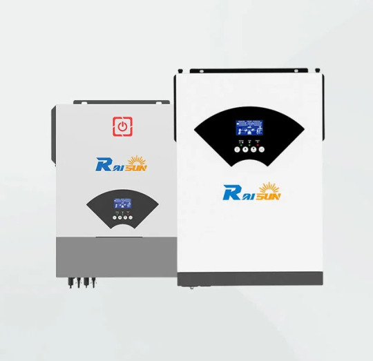
Raisun Solar Inverter & Accessories Wholesale
As a professional solar inverter supplier, Raisun Power supplies the whole set of photovoltaic systems to meet your needs.
The single-phase solar inverters, solar controllers, panels, lithium battery pack, and related accessories are designed to fast installation, easy operation, and smart running.
Raisun is a well-known manufacturer of solar inverters and accessories. They specialize in producing high-quality and efficient solar inverter products wholesale that enable users to harness the power of the sun for their energy needs. The Raisun solar inverters are built with advanced technology that enhances their reliability, efficiency, and performance. Raisun's solar inverters and accessories are reliable, efficient, and designed to meet the energy needs of users in different settings. They are an excellent choice for both residential and commercial solar power systems.
Types of Raisun Solar Inverter Products
Solar Inverter
Solar inverter is a conversion device that converts the DC power generated by solar cells into AC power. It makes the voltage, frequency and waveform of the converted AC power consistent with the voltage, frequency and waveform of the power system AC power to meet the needs of various AC power devices, equipment power supply and grid-connected power generation.
Hybrid Solar Inverter
Pure Sine Wave Inverter
3 Phase Off Grid Inverter
PV Inverters
Solar Inverter Accessories
Solar inverter accessories are essential components that complement the performance of the solar inverters in a solar power system.
Inverter Cable and Accessory
Lithium Battery LiFePO4
Solar Panel
Solar Charge Controller
Why Choose Raisun As Your Solar Inverter & Accessories Company?
STABLE PERFORMANCE
In different working temperatures and working environments, the product performance is stable, and the impact of adverse environment is fully considered in product-design; Meanwhile, considering electromagnetic infection and noise, we also set indicators in product to meet different standards and user needs.
STRONG COMPATIBILITY
Different types of inverters on our website provided by our solar inverter factory cannot only be compatible with solar panels, solar controllers, batteries, and accessories of the whole solar system under our own brand. It is also compatible with different components of photovoltaic inverter systems in other brands.
HIGH SECURITY
Inverter is most sensitive to over-current and short circuit of external circuit. Therefore, the automatic protection of overvoltage, overcurrent and short circuit are the basic measurements to ensure the safe operation of the inverter. Raisun Power inverter has not only overheat protection function when the temperature rise exceeds the specified maximum-limited, but also including short circuit and phase loss protection function.
EASY OPERATION
Each set of solar inverter products will be provided with operating instructions and installation instructions. The equipment connection and installation need to be carried out in strict accordance with the requirements of the instructions. These installation and operation are easy to understand.
DIVERSIFIED CUSTOMIZATION
For each model of solar inverters, solar panels, solar controllers and Lithiunm Batteries, we welcome customization, including not only the LOGO customization, but also the shell color and LOGO customization.
Advanced Raisun Solar Inverter Products & Accessories Technology
Special designers make appearance designs, and design circuit board and inside structure of the whole product;
Automatic machine to make circuit and PCB;
Electrician SMT patch to assemble the parts;
Transistor Tracer to make testing.
1 note
·
View note
Link

#1-12 Layer Rigid-Flexible PCB#PCB Assemble Manufacturer#Multilayer PCB Assemble Manufacturer#China PCB Assemble Manufacturer#Automatic PCB Assemble Factory
0 notes
Text
OEM Electronics Manufacturing in 4 Basic Steps
Electronics manufacturing is considered by many as high-tier level manufacturing challenge. The process of design, assembly, production and testing of electronic components along with PCBs are complex tasks not all electronics manufacturing companies can perform themselves. Using an OEM electronics company is the perfect example of a company who does not fully engage in the complex world of electronics yet end up with electronic products for them to sell or market. They simply let the OEM factories manufacture products on their behalf and all they have to do is introduce ideas and designs. Check here what an Original Equipment Manufacturer actually is. Private and white label electronics companies offer different advantages in the field of electronics manufacturing. You can't introduce your own ideas but have to work with what those companies offer. This is also the reason why OEM contract manufacturing companies in the electronics industry are prevalent. More creative designs are a clear trend in electronics manufacturing. Most electronics manufacturing companies create their electronic product designs then submit these to OEM electronics manufacturers for services such PCB assembly and testing. This way, they only pay for PCB assembly and testing and not pay for the entire electronics manufacturing development process. Aside from the basic services, OEM electronics manufacturers also offer additional services such as PCB etching, board tweaking and redesign etc. However, for private and white label electronics, things are much simpler since you just purchase ready-made electronic devices and brand them.

Step 1: Electronics & Product Design
Product design involves open communication between the client and manufacturer. Most of the time, the manufacturer will ask the client/customer for a concept and they work off of it. A lot of back and forth with suggestions and specifications until the final design is created. This occurrence usually happens if the OEM electronics company do not have graphic design skills to create the layout design or 3D model of the product. Some OEM electronics manufacturing companies are usually staffed with graphic designers to take care of design tasks.

Step 2: Prototyping
Once the design is ready, it now enters the product development stage with the main objective of having a product prototype at the end of the line. After noting down all of the details and specifications for the electronic product, the OEM electronics company will work on the project and complete it as conceived. Extensive research and brainstorming will be done before they integrate into actual manufacturing process to keep risks at a minimum and avoid wasting time and money. The product prototype should be a perfect replica of the design template including specs and details.

Step 3: Product Testing
An electronic prototype which serves as the product replica is going to be the tested in its different facets in multiple times. The goal is to ensure the product meets safety precautions and quality standards with its full functionality. Most OEM electronics manufacturing companies have laboratories designed for product testing and failure investigation. The engineers who conduct these tests will also take advantage of these as a research and development process for future electronic designs related to the current model. Advanced testing procedures include optical inspection which automatically analyze the PCB for issues and defects on the computer. Broken traces, patches, etching issues and improper hole locations are easily detected through automated optical inspection. Another important type of testing process is environmental testing wherein the product is exposed to its intended environment and check if it reacts to the environment’s temperature, humidity, air pressure among other factors to test its durability and resistance. There are several more testing procedures such as functional testing, in-circuit testing, x-ray testing and a lot more depending on the nature of the product. All of these testing procedures will be performed on the product as part of the quality control program and ensure it is in its top form for mass production.

Step 4: Mass Production
Electronic manufacturing is usually divided on to two major areas with mass production capabilities: PCB manufacturing and electronic product manufacturing. 1. PCB Manufacturing There are electronics manufacturing companies who specialize in ODM PCB manufacturing but are limited to this specialty alone and are no longer capable of creating the mold, packaging or case of the electronic product. PCB manufacturing is the task which involves the most electronic knowledge since the printed circuit board houses all of the electrical components, circuits and processors. Electronic manufacturing companies who specialize in ODM PCB manufacturing are most likely staffed with electrical engineers and electronics experts. On the other hand, OEM PCBs are mostly done by the companies themselves. 2. Electronics Product Manufacturing PCB manufacturing is a sub-process of the actual electronics product manufacturing. This is the part wherein the case of the product which houses the PCB itself is created along with other aspects of the product such as aesthetics and functionality. If there are electronics manufacturing companies who specialize in ODM PCB manufacturing alone, there are also companies who only specialize in this area of electronic manufacturing as well. If you notice in OEM electronics these days, none of them have complete departments to deal with the entirety of the electronic manufacturing process. For startups and mid-sized electronics manufacturers, some aspects of the electronic manufacturing are outsourced to other companies to delegate time and expenses unlike with private label electronic manufacturers who simply purchase ready-made electronic designs. Specialty Production Specialized electronics manufacturers can also provide specialty production techniques such as quick turn production, PCB assembly and cabling services. Quick turn production is an instant approach to production aspects like OEM PCB assembly wherein they can assemble the board in 2-3 days upon receiving all of the required electrical components. Cabling services is a special service which focuses exclusively on wires and circuitry.
Conclusion
Electronics manufacturing follows the same manufacturing process such as other product types like garments, plastics and chemicals. The biggest difference are the sub-processes involved in each step which further complicates the entire process due to its specific expertise and knowledge needed for the tasks. The market trend for consumer electronics is still great in the near future. In the aspect of mass production, PCB manufacturing and the actual electronic product manufacturing are both fields which require different skill sets and expertise. The wide range of skills needed within the OEM and ODM electronic manufacturing line is what makes this industry much more complex compared to the others. Hiring employees who are skilled in all of these departments will be tough to find in a very competitive industry and market. Read the full article
2 notes
·
View notes
Text
Top Trends in PCB Assembly for 2025

Top Trends in PCB Assembly for 2025
PCBs are the heart of the modern world. Whether it's household equipment, industrial equipment, or defense ordnance, printed circuit boards are running everything. With new developments, the global scene of PCB manufacturing is changing rapidly. Using the newest technologies is not only a great concept, but staying competitive depends on it as well. From downsizing to AI-driven manufacturing, 2025 promises to bring major breakthroughs along with making advancements in current technologies that will change the way Printed Circuit Boards (PCBs) are manufactured.
This article will walk you through some key industry trends that will sketch the future of PCB assembly.
5 Key Trends in PCB Assembly to Follow in 2025
As the world is moving towards manufacturing more complex products and adopting advanced technologies, the PCB assembly industry is also observing several key trends. Here are a few noteworthy trends to follow.
1. Shrinking is in High-Density Interconnections: HDI and Miniaturization
Think about our daily gadgets, such as wearables, Internet of Things devices, and sophisticated medical electronics. These devices need robust and small PCBs, and therefore, in these spaces, High-Density Interconnect (HDI) technology excels. HDI lets electronic gadgets be more powerful despite their compact stature. In what manner? For high-speed applications, it increases signal integrity, lowers component spacing, and permits smaller trace lengths, hence enhancing electrical performance. And it will change the entire PCB manufacturing market.
According to a forecast [1], the HDI PCB market is expected to rise rapidly and, by 2032, will reach almost $40 billion. That makes the direction in which things are heading quite obvious.
2. Smart Factories: Artificial Intelligence and Automation
Like in every other industry, PCB assembly is becoming significantly faster, smarter, and more efficient. Industry 4.0 and manufacturing driven by artificial intelligence lead the push. Think about robotic soldering and pick-and-place robots for fast, more perfect component installation. Artificial intelligence and machine learning have found their way into quality control, that is, for error reduction and flaw detection done automatically. Imagine the Internet of Things, connected production lines, allowing real-time monitoring and predictive maintenance.
3. Bendable and Adaptable: Rigid-flexible PCBs
Flexible and rigid-flex printed circuit boards are becoming more popular in industries such as transportation, aircraft, and healthcare electronics. But you may think, why so? Because of their small size and lightweight nature, they are ideal for manufacturing small, portable electronic devices. They can withstand significant external force and resist bending and vibration. They endure longer with fewer interconnect failures, making them more reliable.
4. Green is Good: Manufacturing Sustainable Circuit Boards
Growing worries about e-waste and carbon footprints force sustainability to the front stage in PCB production. Lead-free soldering, biodegradable and reusable substrates, recyclable materials, and energy-efficient manufacturing procedures will become the focal points in the near future. It's about matching global laws and customer demand as much as it is about environmental responsibility.
5. Printing the Future: 3D Printing in PCB Assembly
Additive manufacturing is revolutionizing PCB manufacturing and streamlining complex multilayer design construction. From this, faster prototyping, reduced material waste, and more customization for specific uses follow. This is a breakthrough for design and development; it will only get more so.
The Final Thought
There are a lot of exciting new possibilities in the PCB assemblyand PCB manufacturing industries. Miniaturization, automation, sustainability, and developments in AI-driven manufacturing will enable you to produce premium printed circuit boards (PCRs) that satisfy future electronics needs. Survival in a dynamic industry depends on keeping ahead of the competitors. By following these trends and wise technology investments, you could set yourself up for success in 2025 and beyond.
Know More: https://www.pcbpower.us/blog/top-trends-pcb-assembly
0 notes
Text
PCB Manufacture: China vs. US
Looking back on your daily life, have you noticed the growth of consumer electronics and automotive industries are affecting your life and work? Accordingly, it also drives the booming market of PCB Manufacture, which is expected to reach an estimated $89.7 billion by 2024 with a CAGR of 4.3% from 2019 to 2024. Much of this market is currently controlled by PCB manufacturer China companies in places like Shenzhen, which is located in Southeastern China. However, the history of PCB booming in the United States can be traced back to 1950, which is far earlier than China entering this market.
So why can PCB Manufacturer China dominates the market rather than the United States? To solve the confusion for PCB procurements about choosing PCB manufacturer China or US instead, we’ve listed the comparison between the United States and China.
Competitive factors of PCB manufacturer China

According to this report, price was the dominant primary competitive factor in Non-U.S PCB manufacturer, accounting for 76 percent of responses, and China was the leading location, accounting for 67 percent of responses.
And the comparative advantages in various costs which result in lower finished bare PCB prices are:
Labor Costs
Material Costs
Equipment Costs
Environmental Compliance Costs
Building Space Costs
R&D Costs
Supplier Chain
Let’s take Shenzhen MOKO Technology Co., Ltd as an example, which is one of the leading SEM PCB manufacturing and PCB assembly factory in Shenzhen, China.
Labor cost: As you know, Shenzhen is a fast-developing city that gathers many high-tech electronics and automotive industries, each company included MOKO requires clear division of labor, and due to the economic level of China compared to US and easier access to skilled workers, the labor cost of MOKO is far cheaper than in US.
Material cost: MOKO Technology was established since 2001, it’s proficient and experienced in manufacturing PCB and PCB assembly, and also established a stable relationship with accountable material supplier. For a PCB manufacturer that aims to win customers with high-quality and after-sale service, there are many audit processes to certified a material supplier, so the long-term relationship with material suppliers saves a lot of cost of MOKO Technology. Of course, it also doesn’t mean that there’s an opportunity for the material supplier to mix some poor material, from the material sourcing to the forming of substrate and the performance testing of the final products, each process is under strict requirements and testing.
Equipment cost: Chinese high-end equipment is constantly replacing the import, recognized and ordered by the famous PCB enterprises at home and abroad as its high-quality and cost-saving, such as laser drilling machine, laser cutting machine, CNC drilling machine, automatic laser imaging system (LDI), vertical continuous electroplating automatic line (VCP), automatic automatic on and off detection. The main PCB special equipment/instrument representative companies in China are Han’s Laser Technology Industry Group Co., Ltd, Zhengye Technology, UCE Group, Shenzhen Mason Electronics Co., Ltd., and Ta Liang Technology Co., Ltd.
R&D Costs: Due to the overall economic and outcome level in China, the educated and experienced Engineers' salaries and R&D equipment, relevant material and tooling are cheaper than in the US.
Supplier chain: As mass PCB production has shifted away from the U.S. towards Asia,especially Shenzhen, so China has the advantage of the industry supply chain.
Forty-five percent of BIS survey respondents stated that a reduction in U.S. companies that manufacture laminate and other circuit-board related materials has created supply problems for them.
Furthermore, Electronic Contract Manufacturing has been known historically to dramatically reduce supply chain costs, in some cases cutting them in half. ECM has made it possible for companies to shed all or most of their internal manufacturing facilities thereby freeing their valuable company resources for other productive business purposes. In some cases, Electronic Contract Manufacturing has enabled companies to operate without the need for internal manufacturing capabilities or internally-managed factories.
Many companies may choose to outsource their well-established longstanding products to an Electronic Contract Manufacturer, thereby allowing for a greater focus on internal operations for newer products of greater complexity which may have higher margins.
Competitive factors of PCB manufacturer US

According to respondents, U.S. bare PCB manufacturers possess the comparative advantage in:
Lead Time
Quality
Performance
Through the comparison of the advantage between PCB manufacturer China & the US, I believe you’ve got a clear idea for choosing the PCB manufacturer between China and the US, so the next thing you should figure out is what you most concerns when choosing a PCB manufacturer.
Cost
Quality
Lead time
MOQ
Design safety
Experience & Expertise
After-sale service
If you’re considering high-volume production and the price is the most essential factor for your market plan, then you should choose a PCB manufacturer in China as it can save you lots of money for other donate or patronage.
And of course the quality should not be ignored, there are many excellent PCB manufacturers in the US with advanced equipment for ensuring the quality and lead time, and if your company is based on the US, maybe it would be convenient for you to visit the company.
But we know, for business, who don’t want to cooperate with a company that can be conformed to both cost and quality? And of course, to establish your long-term relationship with the PCB manufacturer, most of you would choose to start with a prototype or sample, which is a good way to decrease the deficit and finding out the problem before mass production.
So in such a condition, I suggest you find a reputable and certified experienced PCB manufacturer in China.
Located in Shenzhen, China, MOKO Technology is an expert at PCB Manufacturing and PCB assembly since 2001. MOKO covers an area of more than 8,000 square meters, and has over 250 employees, among them, there are 70 engineers for R&D team and 45 overseas sales for the business team.
Cost:
Firstly, based on geography advantage, MOKO Technology can save a lot of costs like material, component sourcing, labor cost and so on.
Secondly, it has a professional complete procedure from the inquiry to shipping. After receiving the inquiry, MOKO Technology has a team to evaluate customers’ requirements and make an optimized scheme for you, for the material, you will be suggested to choose the suitable material that can perform best for the property.
Thirdly, MOKO Technology has the advantage of supplier chain and it’s experienced in EMS with a one-stop service, which only saves you lots of time and money.
Quality:
For the R&D cost, MOKO Technology has hired experienced 70 engineers
Certified in accordance with ISO 9001: 2015, IPC, and UL (PCB factory: E501497 94V-0; PCB assembly factory: E499341) standards
Bare Board 100 % Visual Inspection & AQL on mechanical to IPC-600 Class II or III
Assembly 100% Visual Inspection to IPC-610 Class II or III
Polar TDR Impedance Testing
PCB Board Net List Electrical Testing 100%
Micro-section Evaluation and Reports
PCB Assembly – ICT testing
PCB Assembly – Functional Testing
PCB Assembly – Burn-In-Testing
X-ray for PC board registration
X-ray for BGA and Component Verification
Automated Optical Inspection (AOI)
Lead Time of PCB Assembly:
MOKO provide 2-50 layered PCBs for fabrication, including HDI, Rigid, Rigid-Flex, & flex boards. From low quantity to mass production, with high quality, and quick turn available at a low cost.
And for the monthly capacity, it can manufacturer 30,000 square meters PCB and 400,000 pcs.

There’s no minimum order requirement, and for the sample, MOKO Technology can accept 10 pcs as MOQ.
Design safety:
About this issue, you can never worry about it as MOKO Technology will sign DOD Contracts with ITAR Registered
After-sale service:
Online Tracking
ERP Systematic order process, you can check the production status of the entire purchase order, and the whole product cycle time.
Professional sales:
Whatever problems happening, you can be replied within 24 hours. There are 70 engineers to support you, including PCB design & PCB Layout, hardware design engineering, firmware & software development, and personalization.
One pair one timely customer order status feedback
MOKO Technology Ltd is a premiere turn-key PCB assembly manufacturer. We are dedicated to providing the best client service in the electronics manufacturing business. Your total satisfaction is extremely important to us. We will meet all your needs in PCB design and layout, PCB manufacturing, and circuit board assembly
Products application industries1> LED PCB
MOKO Technology can offer one-stop service for led light electronic parts focusing on ODM/OEM led PCBA, OEM LED control PCBA and OEM LED Driver PCBA.
It can design hardware, firmware, iOS/Android APP, plastic. If you have a Gerber file and BOM list, they also can offer OEM service for you.
What can MOKO Technology do for LED project:
PCB Design & Layout
Reverse Engineering Service
Fast PCB&PCBA Prototyping
Components sourcing
PCB Assembly
Cable, Wire Assemblies, and Housing Assemblies
Cover coating and glue
Loading firmware & function testing and Aging testing
ODM/OEM LED PCBA Service:
MOKO Technology produced lots of led PCBA, for example, UV LED PCBA for medical machine, UV LED PCBA for 3D printer, AC220V driverless led PCBA, AC110V driverless led PCBA, LED PCBA for street light, LED PCBA for tube light, LED PCBA for panel light, COB RGB LED PCBA for pool light, RGB LED PCBA for pixel light, LED PCBA for ceiling light, LED PCBA for traffic light, etc.
LED PCBA Design & Layout Cases:

MOKO Technology Ltd is a highly respected telecom PCB Assembly, telecom PCBA Manufacturer specializing in prototyping and small volume building in the highly complex area or telecom and industrial computing Printed Circuit Board Assembly(PCBA), PCB Assembly, PCB Assembly service for leading OEMs.
Telecom Printed Circuit Boards Applications:
Phone switching systems
Signal boost online systems
Cell transmission and tower electronics
Satellite technology High-speed routers and servers
Wireless industrial and commercial phone technology
Space communications technology
Military communications systems
Video collaboration Information security technology
PBX systems Voice over internet protocol
Latest Telecom PCBA Cases:

To ensure a positive response from “end”-consumers, many customers from MOKO build on the quality and reliability provided from MOKO.
Latest Consumer Electronics PCBA Cases:

MOKO offers world-class, custom-designed solutions for the automotive market including rapid prototyping, test and product development support with the highest level of quality and traceability to meet your unique requirements.
Latest Automotive PCBA Cases:

MOKO Technology Ltd specializes in the medical PCB assembly and medical PCB production for medical companies of all sizes.
The workmanship of MOKO Technology Ltd can be found in many medical devices such as diagnostic imaging equipment, lasers, and handheld dental tools.
Latest Medical PCBA Cases:

For several years, MOKO has worked with a variety of customers in the industrial market segment from sensors, conditioning systems for alternative energy, power monitoring systems, industrial controls as well as others with demanding environmental requirements.
Latest Industrial PCBA Cases:

So after all this research above, I think choosing the most suitable PCB manufacturer according to your concern is a wise choice. Whatever it’s PCB manufacturer China or PCB manufacturer US, make sure you’ve been clear about your concerns and know your supplier well!
For more info about MOKO Technology Co., Ltd, you can visit https://www.mokotechnology.com/
1 note
·
View note
Text
PCB Manufacturer China and PCB Manufacturer US
Looking back on your daily life, have you noticed the growth of consumer electronics and automotive industries are affecting your life and work? Accordingly, it also drives the booming market of PCB Manufacture, which is expected to reach an estimated $89.7 billion by 2024 with a CAGR of 4.3% from 2019 to 2024. Much of this market is currently controlled by PCB manufacturer China companies in places like Shenzhen, which is located in Southeastern China. However, the history of PCB booming in the United States can be traced back to 1950, which is far earlier than China entering this market.
So why can PCB Manufacturer China dominates the market rather than the United States? To solve the confusion for PCB procurements about choosing PCB manufacturer China or US instead, we’ve listed the comparison between the United States and China.
Competitive factors of PCB manufacturer China

According to this report, the price was the dominant primary competitive factor in Non-U.S PCB manufacturer, accounting for 76 percent of responses, and China was the leading location, accounting for 67 percent of responses.
And the comparative advantages in various costs which result in lower finished bare PCB prices are:
Labor Costs
Material Costs
Equipment Costs
Environmental Compliance Costs
Building Space Costs
R&D Costs
Supplier Chain
Let’s take Shenzhen MOKO Technology Co., Ltd as an example, which is one of the leading SEM PCB manufacturing and PCB assembly factory in Shenzhen, China.
Labor cost: As you know, Shenzhen is a fast-developing city that gathers many high-tech electronics and automotive industries, each company included MOKO requires clear division of labor, and due to the economic level of China compared to US and easier access to skilled workers, the labor cost of MOKO is far cheaper than in US.
Material cost: MOKO Technology was established since 2001, it’s proficient and experienced in manufacturing PCB and PCB assembly, and also established a stable relationship with accountable material supplier. For a PCB manufacturer that aims to win customers with high-quality and after-sale service, there are many audit processes to certified a material supplier, so the long-term relationship with material suppliers saves a lot of cost of MOKO Technology. Of course, it also doesn’t mean that there’s an opportunity for the material supplier to mix some poor material, from the material sourcing to the forming of a substrate and the performance testing of the final products, each process is under strict requirements and testing.
Equipment cost: Chinese high-end equipment is constantly replacing the import, recognized and ordered by the famous PCB enterprises at home and abroad as its high-quality and cost-saving, such as laser drilling machine, laser cutting machine, CNC drilling machine, automatic laser imaging system (LDI), vertical continuous electroplating automatic line (VCP), automatic automatic on and off detection. The main PCB special equipment/instrument representative companies in China are Han’s Laser Technology Industry Group Co., Ltd, Zhengye Technology, UCE Group, Shenzhen Mason Electronics Co., Ltd., and Ta Liang Technology Co., Ltd.
R&D Costs: Due to the overall economic and outcome level in China, the educated and experienced Engineers' salaries and R&D equipment, relevant material and tooling are cheaper than in the US.
Supplier chain: As mass PCB production has shifted away from the U.S. towards Asia,especially Shenzhen, so China has the advantage of the industry supply chain.
Forty-five percent of BIS survey respondents stated that a reduction in U.S. companies that manufacture laminate and other circuit-board related materials has created supply problems for them.
Furthermore, Electronic Contract Manufacturing has been known historically to dramatically reduce supply chain costs, in some cases cutting them in half. ECM has made it possible for companies to shed all or most of their internal manufacturing facilities thereby freeing their valuable company resources for other productive business purposes. In some cases, Electronic Contract Manufacturing has enabled companies to operate without the need for internal manufacturing capabilities or internally-managed factories.
Many companies may choose to outsource their well-established longstanding products to an Electronic Contract Manufacturer, thereby allowing for a greater focus on internal operations for newer products of greater complexity which may have higher margins.
Competitive factors of PCB manufacturer US

According to respondents, U.S. bare PCB manufacturers possess the comparative advantage in:
Lead Time
Quality
Performance
Through the comparison of the advantage between PCB manufacturer China & the US, I believe you’ve got a clear idea for choosing the PCB manufacturer between China and the US, so the next thing you should figure out is what you most concern when choosing a PCB manufacturer.
Cost
Quality
Lead time
MOQ
Design safety
Experience & Expertise
After-sale service
If you’re considering high-volume production and the price is the most essential factor for your market plan, then you should choose a PCB manufacturer in China as it can save you lots of money for other donate or patronage.
And of course the quality should not be ignored, there are many excellent PCB manufacturers in the US with advanced equipment for ensuring the quality and lead time, and if your company is based on the US, maybe it would be convenient for you to visit the company.
But we know, for business, who don’t want to cooperate with a company that can be conformed to both cost and quality? And of course, to establish your long-term relationship with the PCB manufacturer, most of you would choose to start with a prototype or sample, which is a good way to decrease the deficit and finding out the problem before mass production.
So in such a condition, I suggest you find a reputable and certified experienced PCB manufacturer in China.
Located in Shenzhen, China, MOKO Technology is an expert at PCB Manufacturing and PCB assembly since 2001. MOKO covers an area of more than 8,000 square meters, and has over 250 employees, among them, there are 70 engineers for R&D team and 45 overseas sales for the business team.
Cost:
Firstly, based on geography advantage, MOKO Technology can save a lot of costs like material, component sourcing, labor cost and so on.
Secondly, it has a professional complete procedure from the inquiry to shipping. After receiving the inquiry, MOKO Technology has a team to evaluate customers’ requirements and make an optimized scheme for you, for the material, you will be suggested to choose the suitable material that can perform best for the property.
Thirdly, MOKO Technology has the advantage of supplier chain and it’s experienced in EMS with a one-stop service, which only saves you lots of time and money.
Quality:
For the R&D cost, MOKO Technology has hired experienced 70 engineers
Certified in accordance with ISO 9001: 2015, IPC, and UL (PCB factory: E501497 94V-0; PCB assembly factory: E499341) standards
Bare Board 100 % Visual Inspection & AQL on mechanical to IPC-600 Class II or III
Assembly 100% Visual Inspection to IPC-610 Class II or III
Polar TDR Impedance Testing
PCB Board Net List Electrical Testing 100%
Micro-section Evaluation and Reports
PCB Assembly – ICT testing
PCB Assembly – Functional Testing
PCB Assembly – Burn-In-Testing
X-ray for PC board registration
X-ray for BGA and Component Verification
Automated Optical Inspection (AOI)
Lead Time of PCB Assembly:
MOKO provides 2-50 layered PCBs for fabrication, including HDI, Rigid, Rigid-Flex, & flex boards. From low quantity to mass production, with high quality, and quick turn available at a low cost.
And for the monthly capacity, it can manufacturer 30,000 square meters PCB and 400,000 pcs.

There’s no minimum order requirement, and for the sample, MOKO Technology can accept 10 pcs as MOQ.
Design safety:
About this issue, you can never worry about it as MOKO Technology will sign DOD Contracts with ITAR Registered
After-sale service:
Online Tracking
ERP Systematic order process, you can check the production status of the entire purchase order, and the whole product cycle time.
Professional sales:
Whatever problems happening, you can be replied within 24 hours. There are 70 engineers to support you, including PCB design & PCB Layout, hardware design engineering, firmware & software development, and personalization.
One pair one timely customer order status feedback
MOKO Technology Ltd is a premiere turn-key PCB assembly manufacturer. We are dedicated to providing the best client service in the electronics manufacturing business. Your total satisfaction is extremely important to us. We will meet all your needs in PCB design and layout, PCB manufacturing, and circuit board assembly
Products application industries1> LED PCB
MOKO Technology can offer one-stop service for led light electronic parts focusing on ODM/OEM led PCBA, OEM LED control PCBA and OEM LED Driver PCBA.
It can design hardware, firmware, iOS/Android APP, plastic. If you have a Gerber file and BOM list, they also can offer OEM service for you.
What can MOKO Technology do for LED project:
PCB Design & Layout
Reverse Engineering Service
Fast PCB&PCBA Prototyping
Components sourcing
PCB Assembly
Cable, Wire Assemblies, and Housing Assemblies
Cover coating and glue
Loading firmware & function testing and Aging testing
ODM/OEM LED PCBA Service:
MOKO Technology produced lots of led PCBA, for example, UV LED PCBA for medical machine, UV LED PCBA for 3D printer, AC220V driverless led PCBA, AC110V driverless led PCBA, LED PCBA for street light, LED PCBA for tube light, LED PCBA for panel light, COB RGB LED PCBA for pool light, RGB LED PCBA for pixel light, LED PCBA for ceiling light, LED PCBA for traffic light, etc.
LED PCBA Design & Layout Cases:

MOKO Technology Ltd is a highly respected telecom PCB Assembly, telecom PCBA Manufacturer specializing in prototyping and small volume building in the highly complex area or telecom and industrial computing Printed Circuit Board Assembly(PCBA), PCB Assembly, PCB Assembly service for leading OEMs.
Telecom Printed Circuit Boards Applications:
Phone switching systems
Signal boost online systems
Cell transmission and tower electronics
Satellite technology High-speed routers and servers
Wireless industrial and commercial phone technology
Space communications technology
Military communications systems
Video collaboration Information security technology
PBX systems Voice over internet protocol
Latest Telecom PCBA Cases:

To ensure a positive response from “end”-consumers, many customers from MOKO build on the quality and reliability provided from MOKO.
Latest Consumer Electronics PCBA Cases:

MOKO offers world-class, custom-designed solutions for the automotive market including rapid prototyping, test and product development support with the highest level of quality and traceability to meet your unique requirements.
Latest Automotive PCBA Cases:

MOKO Technology Ltd specializes in the medical PCB assembly and medical PCB production for medical companies of all sizes.
The workmanship of MOKO Technology Ltd can be found in many medical devices such as diagnostic imaging equipment, lasers, and handheld dental tools.
Latest PCBA Cases:

For several years, MOKO has worked with a variety of customers in the industrial market segment from sensors, conditioning systems for alternative energy, power monitoring systems, industrial controls as well as others with demanding environmental requirements.
Latest Industrial PCBA Cases:

So after all this research above, I think choosing the most suitable PCB manufacturer according to your concern is a wise choice. Whatever it’s PCB manufacturer China or PCB manufacturer US, make sure you’ve been clear about your concerns and know your supplier well!
For more info about MOKO Technology Co., Ltd, you can visit https://www.mokotechnology.com/ and https://www.mokotechnology.com/pcb-manufacturer-china-vs-us/
1 note
·
View note
Text
Company Profile
Company Profile
HX Electronic Technology Company ProfileAs a PCB assembly company, a Chinese national high tech enterprise and SMT electronic technology limited, HX Electronic Technology Co., Ltd. is specialized in full form of PCBA assembly service, including PCB fabrication, components sourcing, SMT, and THT. Our products are widely applied in industrial controllers, medical equipment, telecom devices, environmental protecting equipment, instruments and meters, security system, smart electronic devices, vehicle electronic devices, consumer electronics, and so on.
With a total investment of $10 million and covering an area of more than 10000 square meters, HX Technology now has more than 300 employees, including 50 senior engineering and technical personnel, 50 supply chain management staff, and 30 components sourcing staff amount them. Our professional PCB assembly factory and SMT electronic technology limited are equipped with 6 automatic SMT production lines, 2 THT production lines, 2 assembly lines, and a large number of advanced inspection and testing equipment. Our current daily production capacity is 10 million SMT points /day, 2.5 million THT pieces /day, and 5000 electronics assembly units/day.
HX Technology has established a perfect supplier import and analysis system to ensure our superior advantage of PCBA material quality, lead time, and pricing. Our professional sourcing team can acquire inventory information of remote, unpopular, and short materials, thus presenting the best purchasing solution. We have established a strategic partner relationship with local plastic, metal, and mold suppliers in China, which makes us can provide high quality, fast delivery, low price for special customized material. HX Technology guarantees that all the components are original binding and sourcing traceable.
HX Technology provides fast, professional, and high-quality printed circuit board service, including minimum 6 hours quotation releasing, minimum 2 hours engineer query releasing minimum lead time in 72 hours, minimum 48 hours global express shipment, after-sales problem resolving solution in 2 hours, professional DFM report, and 24 hours online customer service.
HX Technology provides high-quality products by following the ISO production procedure and adopts the IPC class 2 quality surveillance standards. In line with the continuous reforming and innovation of the scientific spirit, with advanced production technology and management philosophy, HX Technology is working hard to provide high-quality products and first-class printed circuit board service for customers all over the world.
https://www.hx-technology.com/company-profile/

0 notes
Text
Printed Circuit Board
There is a wide range of PCB manufacturing services offered by GreensTone. We specialize in manufacturing kinds of PCBs such as FR4 PCB, heavy copper PCB, HDI PCB, High-TG PCB, multi-layer PCB, rigid PCB and etc.
Types of Printed Circuit Board
PCB Capability
GreensTone provides 1-8 layers PCB manufacture, including FR4 PCB, Hi-tg PCB, thick copper PCB, single layer or multi-layer PCB with conventional HASL, Lead-free HASL,Falsh Gold, ENIG (Immersion Gold) OSP(Entek), Immersion Tin, Immersion Silver, Hard Gold and so on.
PCB Surface
Common PCB surface treatment technologies which GreensTone may use when manufacturing PCBs are HASL (hot air solder leveling), organic coating (OSP), electroless nickel/gold, immersion silver, immersion gold, and etc.
FR4 PCB
FR4 is the most important material in the PCB assembly. Electric engineers and technicians normally design PCB boards with the FR4 PCB. There is a big demand for FR4. FR4 printed circuit board is normal and easy to design. The FR4 PCBs are popular as they are cost effective and can be widely used.
High-TG PCB
Normally FR4 Tg is 130-140°, moderate Tg is over 150-160 °, High-Tg is greater than 170°.The higher of Tg, the better performance of PCB moisture resistance, heat resistance, chemical resistance, stability and other characteristics.
Read More
High-TG PCB
Heavy Copper PCB
Thick copper PCBs are characterized by being covered with copper thicknesses from 3oz to 400 µm. These PCBs are used for high current outputs and high thermal management. The heavy copper allows PCB for high currents load and encourages heat radiation.
PCB Capability
PCB Surface
FR4 PCB
High-TG PCB
Heavy Copper PCB
What is PCB?
PCB is the abbreviation of the printed circuit board. PCB composed by insulated baseboard, pads for electronic components and copper foil connecting wires. PCB can replace complex wiring to achieve circuit connection between components in the circuit.
PCB is the motherboard of electronic components. Before the advent of PCB, the interconnection between electronic components was done directly by wires. Today, PCB has been widely used in the electronics industry, due to the PCB tecnology, manual wiring errors can be avoided, and electronic components can be automatically DIP or SMT, automatic soldering, and automatic detection, ensuring the quality of electronic device and improving labor productivity, reduce costs as well.
What Is the Difference Between PCB And PCBA?
PCB is a blank circuit board without any electronic components soldered on. It just composed by baseboard with pads and copper foil connection wires.
PCBA is a complete assembled board with electronic components. We apply surface mount technology and through-hole soldering technology solder the components onto the board. The components are soldered to the board can be SMD, through hole, UBGA, QFN, POP, leadless chips, connectors and terminals.
PCB Manufacture Step by Step
Preproducing engineering checking
Board cutting
Print inner layer
Eych inner layer
AOI
Layer up and bond
Drilling the PCB
Electroless copper deposition
Image teh outer layer
Plating
Etch the outter layer
AOI
Solder mask
Surface finish
Profile
Electrical test
Finial inspection
Packing

0 notes
Text
Flexible PCB assembly services
Electronic manufacturing services Company, OEM, EMS, SMT pick and place line factory, Shenzhen

0 notes
Photo

Industrial experience happens to be one of the most pivotal factors, which separates generic PCB Assemble Manufacturer with the finest one! The experience of a manufacturer showcases the capability of adapting and innovating over the changing course of the most current technology.
0 notes
Text
PCB Assembly and Production Process
Within a printed circuit board electronics assembly / production or manufacturing process there are a number of individual stages. However it is necessary for them all to work together to form an integrated overall process. Each stage of assembly and production must be compatible with the next, and there must be feedback from the output to the input to ensure that the highest quality is maintained. In this way any problems are detected quickly and the process can be adjusted accordingly.
PCB assembly process overview
The various stages in the PCB assembly process including adding solder paste to the board, pick and place of the components, soldering, inspection and test. All these processes are required, and need to be monitored to ensure that product of the highest quality is produced. The PCB assembly process described below assumes that surface mount components are being used as virtually all PCB assembly these days uses surface mount technology.
Solder paste: Prior to the addition of the components to a board, solder paste needs to be added to those areas of the board where solder is required. Typically these areas are the component pads. This is achieved using a solder screen. The solder paste is a paste of small grains of solder mixed with flux. This can be deposited into place in a process that is very similar to some printing processes. Using the solder screen, placed directly onto the board and registered in the correct position , a runner is moved across the screen squeezing a small mount of solder paste through the holes in the screen and onto the board. As the solder screen has been generated from the printed circuit board files, it has holes on the positions of the solder pads, and in this way solder is deposited only on the solder pads. The amount of solder that is deposited must be controlled to ensure the resulting joints have the right amount of solder.
Pick and place: During this part of the assembly process, the board with the added solder paste is then passed into the pick and place process. Here a machine loaded with reels of components picks the components from the reels or other dispensers and places them onto the correct position on the board. The components placed onto the board are held in place by the tension of the solder paste. This is sufficient to keep them in place provided that the board is not jolted. In some assembly processes, the pick and place machines add small dots of glue to secure the components to the board. However this is normally done only if the board is to be wave soldered. The disadvantage of the process is that any repair is made far more difficult by the presence of the glue, although some glues are designed to degrade during the soldering process. The position and component information required to programme the pick and place machine is derived from the printed circuit board design information. This enables the pick and place programming to be considerably simplified.
Soldering: Once the components have been added to the board, the next stage of the assembly, production process is to pass it through the soldering machine. Although some boards may be passed through a wave soldering machine, this process is not widely used for surface mount components these days. If wave soldering is used, then solder paste is not added to the board as the solder is provided by the wave soldering machine. Rather than using wave soldering, reflow soldering techniques are used more widely.
Inspection: After the boards have been passed through the soldering process they are often inspected. Manual inspection is not an option for surface mount boards employing a hundred or more components. Instead automatic optical inspection is a far more viable solution. Machines are available that are able to inspect boards and detect poor joints, misplaced components, and under some instances the wrong component.
Test: It is necessary to test electronic products before they leave the factory. There are several ways in which they may be tested. Further views of test strategies and methods may be found on the "Test and Measurement" section of this website.
Feedback: To ensure that the manufacturing process is running satisfactorily, it is necessary to monitor the outputs. This is achieved by investigating any failures that are detected. The ideal place is at the optical inspection stage as this generally occurs immediately after the soldering stage. This means that process defects can be detected quickly and rectified before too many boards are built with the same problem.
The PCB assembly process for the manufacture of loaded printed circuit boards has been considerably simplified in this overview. The PCB assembly and production processes are generally optimized to ensure very low levels of defects, and in this way produce the highest quality product. In view of the number of components and solder joints in today's products, and the very high demands placed on quality, the operation of this process is critical to the success of the products that are manufactured.
0 notes