#Ceramic Substrate Pcb
Text
Maximize Performance with Ceramic PCB Technology
Experience the unmatched reliability and performance with Hitech Circuits Co. Limited's Ceramic PCB solutions. With over 10 years of experience designing and fabricating ceramic substrates, we are an industry-leading supplier in China committed to quality, service, and technical expertise. Our meticulously crafted Ceramic PCBs are extremely versatile and can replace a complete traditional PCB with a less complex design and enhanced performance. Designed with expertise, our Ceramic PCBs offer exceptional thermal conductivity and electrical insulation, making them ideal for demanding applications. Hitech Circuits Co. Limited also offers Ceramic Substrate PCB for your printed circuit board’s needs. For more details about Ceramic PCBs, contact us today!

1 note
·
View note
Text
BST Ceramic PCB: Your partner in Ceramic PCB solutions
In demanding electronic applications where performance is essential, traditional PCBs often fall short. That is where ceramic PCBs come in, offering a leap forward in reliability, thermal management, and overall efficiency.
At BST Ceramic PCB, we specialize in the manufacturing of high-performance ceramic circuit boards. Our advanced technology utilizes ceramic materials as the base for these PCBs, offering advantages over traditional FR-4 epoxy boards.
What sets ceramic PCBs apart?
Unlike conventional PCBs, ceramic core PCBs utilizes a ceramic base material, such as alumina or aluminium nitride. This ceramic substrate PCB construction brings a host of advantages:
Exceptional thermal conductivity: Dissipate heat rapidly and efficiently, even in high-power applications.
High-frequency performance: Ideal for applications requiring high signal speeds and minimal signal loss.
Dimensional Stability: Resistant to wrapping and shrinking, ensuring consistent performance in extreme environments.
Chemical resistance: Withstand harsh chemicals and environments, ensuring long-term reliability.
BST Ceramic PCB: Your partner in Ceramic PCB solutions
We offer a comprehensive range of ceramic base PCB solutions, including:
High temperature PCBs
High voltage PCBs
RF and Microwave PCBs
LED PCBs
Our team of experts will work closely with you to understand your unique requirements and deliver custom ceramic substrate PCBs that exceed your expectations.
Applications Across Industries
Our ceramic PCBs cater to a diverse range of industries due to their unique properties:
Telecommunications: Ideal for high-frequency applications like RF amplifies and microwave components.
Automotive: Withstand extreme temperatures and vibrations, making them perfect for engine control units and power electronics.
MedicalElectronics: Deliver reliable performance in demanding medical devices like pacemakers and defibrillators.
AerospaceandDefense: Function flawlessly in harsh environments for applications in satellites, radar systems, and military equipment.
Experience the BST Ceramic PCB Difference
Bestquality: We adhere to the highest industry standards to ensure superior product performance and reliability.
Cutting-EdgeTechnology: Our best facilities allow us to manufacture complex ceramic circuit boards with precision.
Customer-Centricapproach: We are committed to providing exceptional customer service and support throughout the entire process.
Contact us today to discuss your project requirements and experience the exceptional performance and reliability of BST Ceramic PCBs. Enhance your electronic devices to the next level with our latest technology.
0 notes
Text

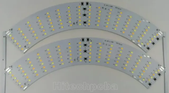
Ceramic PCB Manufacturing--Hitechpcba
Ceramic PCB board is also called ceramic substrate or ceramic circuit board, ceramic copper coated plate, ceramic substrate refers to the copper foil directly bonded to alumina (Al2O3) or aluminum nitride (AlN) ceramic substrate or other ceramic substrate surface (single or double) on the special process board. The ultrathin composite substrate has excellent electrical insulation performance, high thermal conductivity, excellent soft brazing and high adhesion strength, and can be etched into a variety of graphics like PCB board, with great current-carrying capacity. Therefore, Ceramic PCB board has become the basic material of high power electronic circuit structure technology and interconnection technology.
Ceramic PCB Manufacturing & Assembly – One-stop service The ceramic substrate (ceramic PCB) refers to a special process board in which a copper foil is directly bonded to a surface of an alumina (Al2O3 ) or aluminum nitride (AlN) ceramic substrate (single or double-sided) at a high temperature. The ultra-thin composite substrate produced has excellent electrical insulation properties, high thermal conductivity, excellent solderability, and high adhesion strength, and can etch various patterns like a PCB board, and has a large current carrying current ability.
The advantages and disadvantages of Ceramic PCB
(1) Ceramic PCB board has very good thermal conductivity and insulation performance. Ceramic PCB board is made of ceramic substrate, ceramic substrate itself has very good insulation and thermal conductivity, thermal conductivity of 25~230w, insulation resistivity is 10 minus 14 square, visible insulation performance is very good.
(2) The dielectric constant of ceramic PCB board is very low, the dielectric loss is small, has very good high frequency performance, the dielectric loss of alumina ceramic PCB board is less than 0.0003@1MHz, the dielectric loss of aluminum nitride ceramic PCB board is less than 0.0005@1MHz. Low dielectric loss, high frequency performance, is widely used in the field of high frequency communication.
(3) Ceramic PCB bonding force is strong, using bonding technology, copper foil will not fall off.
(4) Ceramic PCB has large on-board flow, 100A current continuously passes through 1mm0.3mm thick copper body, and the temperature rises about 17℃; when 100A current continuously passes through the 2mm0.3mm thick copper body, the temperature rises only about 5℃.
(5) Ceramic PCB board is with high temperature resistance, corrosion resistance, environmental protection, can work in a very complex environment, long-term high frequency, long service life.
Disadvantages: fragile, scrap rate is high, this is one of the main short comings of ceramic PCB board, which leads to the production of a small area of the circuit board, the general size is less than 120mm, special custom 200mm,230mm, the general price is more expensive, the board cost is higher. In addition, because ceramic PCB board is made of ceramic material, it does not have better toughness like FR4 board, so it can make more than one meter long and wide. Another point is that the price is expensive, the requirements of electronic products are more and more rules, ceramic circuit boards are still used in some relatively high-end products, low-end products will not be used.
With over 15 years of experience in the electronic industry we are committed to producing custom ceramic PCBs that meet up with the various electronic devices at hand.
0 notes
Text

LiDAR (Light Detection And Ranging, referred to as “LiDAR”) measurement is a system that integrates three technologies: laser, GPS (Global Positioning System), and IMU (Inertial Measurement Unit, inertial measurement unit), used to obtain data and Generate accurate DEMs (Digital Elevation Models). The combination of these three technologies can highly accurately locate the spot of the laser beam on the object, and the ranging accuracy can reach the centimeter level. The biggest advantage of lidar is accurate, fast, and efficient operation.
Therefore, choosing a high-quality ceramic substrate not only helps to solve the problem of thermal and electrical separation of laser emitters, but also provides stable heat dissipation and electrical performance, providing reliable support for efficient operation and performance improvement of laser emitters. In the development of lidar technology, ceramic substrates play an increasingly important role, providing key support for performance breakthroughs and innovations in laser transmitters. We are witnessing a revolution in the auto industry brought about by China’s autonomous driving assistance systems.
If you are designing a ceramic PCB and seeking a reliable manufacturer, welcome to leave you message or contact us directly.
0 notes
Text
LED PCB Assembly
What is the LED Circuit Board assembly?
Generally, LED PCB assembly is considered to be a circuit board that has the LED components soldered to it. The LED is soldered to the printed circuit board and features a chip that creates the light as electrically connected. A thermal heat sink and a ceramic base are used to bond the chip. Not all the PCB products can be used in Led industry, as an LED PCB is easy to create a high volume of heat, but making it hard to cool with traditional methods. For this reason, metal core PCB is widely used in LED application because of their enhanced ability to dissipate heat, especially aluminum pcb is often used to fabricate PCB for LED lights.
We’ve had great LED PCB assembly experiences with top LED chips to brand such as Cree, Luxeon, Osram, Nichia, Lumileds, MLS, EVERLIGHT, Samsung, LG, Seoul., etc. PCB LED lights can be incorporated into numerous lighting applications due to their combination of excellent energy efficiency, low cost and maximum design flexibility.

Application of LED PCB Assembly
Hitechpcba serves customers in different industries, providing highly reliable and innovative LED PCBs for various applications:
• Horticulture light LED PCB Assembly
• LED controller PCB Assembly
• Computer LED display and indicators
• LED lights PCB Assembly for medical use
• Automotive LED PCBs Assembly include PCBs for brake lights and headlights
• Street lighting LED PCB Assembly
• Flashlights and camping accessories
• Traffic light PCB Assembly
• Commercial lighting LED PCB Assembly
LED PCB Assembly specification
Number of layers for LED PCB
These layers are made up of aluminum and magnesium, but now have Copper base material and Ceramic base materials for LED PCB industry, we can meet it.
Aluminum LED PCBs stand out among other PCBs because it has a good insulation characteristic and has a better machinery performance, the cheap cost is one important factor too.
Types of layers for LED PCB Assembly
Normally, the base layer is made using aluminum alloy metal.
This aluminum alloy substrate used in making the base makes it ideal for through-hole technology which transfers and dissipates heat.
A thermal insulation layer is made using some ceramic polymer which has good viscoelasticity characteristics.
It is highly heat resistant and protects the PCB against heat and mechanical stress.
The circuit layer, which is covered by a copper foil which can range from one to ten ounces.
LED Board type- single or in panel
Some boards are shapeless. For this reason, LED PCB panels are used. This reduces time, labor production and testing time.
Some LED PCB Assembly is done on a single board while others are done on panel boards.
LED PCB Assembly Process
Roughly, the PCBA process can be divided into theses phases: soldering paste printing > SMT (surface mounted technology) > reflow soldering > AOI (automated optical inspection)> THT (through-hole technology) > wave soldering > touch-up and cleaning > IC-programming > FCT (functional tests) > aging testing.
Below we show you the process.
Step1. Summarizing Project Information
Before contacting your supplier, make sure you have all the project information. Suppliers will need info following for quoting LED PCB assembly:
Gerber
BOM
LED PCB specification
Quotation quantity
Once you have gathered these information, you can contact us and request for a quote.
Of course, you can also provide the schematic, LED PCB Assembly pictures and even samples to us. The more details they have, the more accurate the supplier’s quotation will be.
Step2. Discussion and details about custom LED PCB Assembly
Different projects will have different requirements. Remember the special requirements mentioned in step 1? That’s going to be the focus of this session. Equipment and engineering capacity will not be identical between suppliers. Make sure your supplier has the equipment to produce and assemble major components and the corresponding testing capabilities.
For example, some vendors don’t have X-ray testing equipment, which means they can’t check the mount quality of BGA chips. Outsourcing this step will increase risk and cost. That’s what you don’t want.
Also, pay attention to time taken by the supplier to quote. Motherboards often contain hundreds or even thousands of components, and they are supplied by different manufacturers. To ensure the quality of the components, the supplier sourcing team will make multi-inquiries from these manufacturers or authorized suppliers to match customer’s requirement, which usually takes 2-3 business days, and even longer for some scarce chips. Therefore, if your project is complex and the supplier quotes you within few hours, double check with them.
Step3. Sample and feedback
After confirming the PI, the supplier will usually provide pre-production samples for your approval. At the same time, the supplier will also confirm with you the logistics plan of the bulk goods. Make sure they understand your shipping requirements, including details on packaging, customs clearance, taxes, etc.
For us to have a successful LED PCB Assembly process, its functions must be defined. Compliance requirement is defined to reduce the effect when components are selected.
The Bill of Materials is then generated from the information installed on the LED PCB.
All this information is used to assemble components which are identified from MOB to the LED PCB.
After that, the routing of traces is determined to each component, based on the size, shape of the circuit board and location of connectors.

Hitech Circuits is trusted by thousands of electronic engineers on their LED PCB assembly projects, from consumer, led bulb to precisely medical LED light, we can help you from the beginning of design stage; From commercial flood LED to industrial high power LED, from automotive LED to military LED, Venture is the perfect place for your LED PCB assembly requirement.
Hitech Circuits has been participated in hundreds and thousands of LED lighting projects, by providing LED PCB and also LED PCB assembly service.
Our LED PCB assembly had covered both ends of the Lighting Class LED size spectrum, assembling some of the largest (2 meter long boards) and some of the smallest LED Lighting applications which used in Medical Endoscopes.
LED PCB Assembly is very crucial in the current industrial development. Many electrical devises are being innovated and the old once being improved.
LED PCBs are useful due to the fact that they are made using materials that can transfer and dissipate heat. This characteristic increases device durability.
The world is changing with new technology, especially PCB technology that plays an essential role in the application of LED circuits. And the LED industry is taking advantage of this technology and growing faster.
As a full feature PCB solutions provider with more than a decade of experience, we're capable to provide LED PCB fabrication, components procurement and LED PCB assembly all under one roof. We can work with you to develop metal core PCB, aluminum circuit boards customized to your specific applications. We feature competitively priced PCBs made with standard FR-4 material that includes a thermal aluminum clad layer that will efficiently dissipate heat, keep all LED PCB components cool and significantly enhance the performance of your products.

LED pcb board, LED pcb assembly
LED with its advantages of high brightness, high efficiency, low heat, long life, is considered the most development potential in the 21st century lighting. In the market and policy driven by the rapid development of the domestic LED industry blowout has formed a relatively complete industrial chain, including the production of epitaxial wafers, chip preparation, packaging, integration, LED application. In 2010, China's LED industry scale, up from $ 827 billion in 2019 to 220 billion yuan, an annual growth rate of over 70%, higher than the 50% level of growth of the global LED lighting industry output value. Among them, the middle and lower reaches of the most complete industrial chain, accounting for 90% of the overall percentage of the GDP.Chinahas become the world's leading LED manufacturing base and important application market.
To further promote the technological innovation of the LED industry, construction and wide application of independent industry chain, China Electronic Appliance Corporation and industry associations to organize the theme of "Focus on the core energy LED Exhibition will be held November 9-11, 2010 in Shanghai International Expo Center and the 78th China Electronics Fair over the same period will be held will create from raw materials, epitaxial wafers, chip, LED bracket, LED accessories, LED packaging and supporting materials, the LED backlight upstream firm to the upstream and downstream enterprises of the display, lighting, landscaping, decorative lighting, traffic lights, automotive lighting, special lighting, to the equipment, instrumentation, software, finance, consulting and other service enterprises and technological exchanges and market trading platform, help the domestic industry sustained and healthy development, and promote the steady expansion of the LED application market.
In the LED industry chain upstream of the epitaxial wafers and LED chips accounted for 70% of the profits of the whole industry, and technology-intensive, capital-intensive, where the core technology of the LED. Well-known epitaxial wafer and chip production enterprises will be exhibited a number of energy-efficient, low heat, cost-effective LED products, many of whom have excellent products of international advanced level.
LED electronic pcb assembly��manufacturing 100% Original LED Chip with one-stop in-house pcba services
3 notes
·
View notes
Text
Optimized SMT Circuit Board and PCB Assembly Manufacturing: A Guide to Modern Electronics Production
In the ever-evolving world of hardware, the SMT (Surface Mount Technology) circuit board and PCB (Printed Circuit Board) assembly fabricating forms have gotten to be progressively vital. These advances not as it were empower the creation of smooth, compact, and high-performance electronic gadgets but moreover play an imperative part in the victory of different businesses, from shopper hardware to aviation and beyond.
Understanding the SMT Circuit Board Manufacturing Process
The SMT circuit board fabricating prepare includes the situation and fastening of electronic components specifically onto the surface of a printed circuit board. This approach offers a few focal points over conventional through-hole innovation, including:
1. Miniaturization: SMT components are by and large littler and more compact than their through-hole partners, permitting for the creation of littler and more lightweight electronic devices.
2. Increased Productivity: The robotized pick-and-place machines utilized in SMT fabricating can collect components on a circuit board much quicker than manual patching, moving forward generation efficiency.
3. Enhanced Unwavering quality: The patch joints in SMT gatherings are regularly more dependable and less inclined to disappointment than those in through-hole designs.
4. Cost Investment funds: SMT fabricating frequently decreases the in general fetched of electronic components and congregations, making them more open to a more extensive run of businesses and consumers.
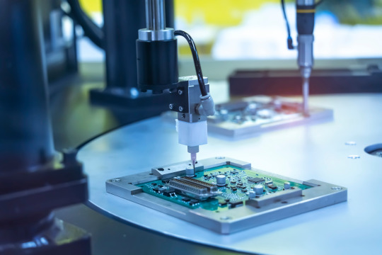
The PCB Assembly Manufacturing Process
The PCB Assembly Manufacturing includes the integration of different electronic components onto a printed circuit board to make a useful electronic gadget. This prepare ordinarily incorporates the taking after steps:
1. PCB Manufacture: The to begin with step is the generation of the printed circuit board itself, which includes the creation of copper follows, cushions, and other highlights on a non-conductive substrate, such as fiberglass or ceramic.
2. Component Situation: Once the PCB is manufactured, electronic components, such as resistors, capacitors, coordinates circuits, and connectors, are put onto the board utilizing computerized pick-and-place machines or manual assembly methods.
3. Soldering: After the components are set, they are fastened onto the PCB utilizing procedures like wave patching, reflow patching, or specific fastening, depending on the particular necessities of the assembly.
4. Inspection and Testing: The amassed PCB is at that point assessed and tried to guarantee that all components are legitimately associated, and the circuit is working as intended.
5. Finishing Forms: Depending on the application, the PCB may experience extra wrapping up forms, such as conformal coating, embodiment, or the expansion of warm sinks or shielding.
The Significance of SMT Circuit Board andPCB Assembly Manufacturing
The SMT Circuit Board and PCB assemblyfabricating forms are basic for the generation of a wide run of electronic gadgets, from shopper hardware to mechanical hardware and past. These advances empower the creation of compact, lightweight, and profoundly solid electronic components and congregations, which are basic for assembly the ever-increasing request for progressed, feature-rich electronic devices.

Furthermore, the SMT circuit board and PCB gathering fabricating forms play a pivotal part in the competitiveness of different businesses, as they permit for the quick and cost-effective generation of electronic items. This, in turn, leads to progressed time-to-market, diminished fabricating costs, and upgraded item quality, all of which are basic for keeping up a competitive edge in today's worldwide marketplace.
Conclusion
The SMT circuit board and PCB assemblyfabricating forms are at the heart of the advanced gadgets industry, empowering the creation of imaginative and mechanically progressed items that proceed to change our world. By understanding the complexities and benefits of these forms, producers and originators can use these advances to make items that are not as it were outwardly engaging and profoundly useful but too cost-effective and dependable.
0 notes
Text
Understanding Special PCB: The Backbone of Customized Electronics
In today’s rapidly evolving technology landscape, Special PCBs (Printed Circuit Boards) have become a cornerstone in customized electronics, playing a pivotal role in industries like aerospace, healthcare, telecommunications, and automotive. These specialized boards are tailored to meet unique design requirements and performance standards that exceed conventional PCB capabilities.

What are Special PCBs?
Special PCBs are distinct from standard circuit boards due to their specific materials, layout designs, and intended applications. These boards are used for devices that operate in harsh environments, require higher performance, or need to be compact and efficient. Whether it’s rigid-flex PCBs, aluminum-based PCBs for LED lighting, or multilayer boards, special PCBs are designed to cater to niche market needs.
The Role of PCB Manufacturing in Special PCBs
Creating special PCBs demands cutting-edge PCB manufacturing processes and advanced technology. The production of these PCBs involves multiple stages, including:
Design and Prototyping: Advanced software is used to design the layout, followed by the creation of prototypes for testing.
Material Selection: Special materials, such as ceramic, polyimide, or copper-clad laminates, are chosen based on the application’s specific needs.
Precision Assembly: The manufacturing of special PCBs requires high-precision assembly techniques like surface mount technology (SMT) and through-hole assembly to ensure reliability and performance.
PCB Board Makers: Experts in Customization
Leading PCB board makers like Shenzhen Shuoqiang Electronics (SQPCB) specialize in delivering high-quality special PCBs tailored to individual specifications. With state-of-the-art manufacturing facilities, SQPCB can handle small-scale prototype projects or large-scale production orders, ensuring precision, durability, and performance.
Assembly of Special PCBs
PCB manufacturing assembly is a critical phase where components are mounted onto the PCB substrate. For special PCBs, the assembly process requires meticulous attention to detail due to their complexity. Whether it’s high-density interconnect (HDI) boards or PCBs with intricate multilayer designs, the right assembly process ensures the optimal functionality of the circuit.
The PCB assembly process typically involves:
Soldering Components: High-quality soldering methods, like reflow soldering, are used to attach components to the board accurately.
Testing and Quality Control: After assembly, PCBs undergo rigorous testing to ensure they meet quality standards and perform as intended in their specific applications.
Why Choose SQPCB for Special PCB Manufacturing?
SQPCB stands out as a trusted PCB board maker for several reasons:
Customization: Their team of experts works closely with clients to deliver customized special PCBs tailored to specific requirements.
Advanced Technology: They use the latest tools and technologies to ensure the highest standards of manufacturing and assembly.
Quality Assurance: With a robust quality control process, every PCB manufactured by SQPCB is rigorously tested to ensure reliability and performance.
Competitive Pricing: SQPCB offers cost-effective solutions without compromising on quality, making them a preferred partner for businesses of all sizes.
Conclusion
Special PCBs are critical in driving innovation in various sectors, offering unmatched performance and adaptability for custom electronic devices. By partnering with experienced PCB board makers like SQPCB for PCB manufacturing and assembly, businesses can ensure the production of high-quality, reliable, and efficient special PCBs for their unique applications.
#Special PCB#pcb manufacturing#customize pcb#flex pcb#pcb manufacturers#multilayer pcb#advertising#rigid flex pcb#business
0 notes
Text
PCB Assembly Solutions for High-Reliability Applications: What to Look For

In industries where safety and performance are paramount—such as aerospace, medical devices, automotive, and military—reliable and robust electronic systems are crucial. The quality and reliability of these systems largely depend on the precision and effectiveness of the PCB (Printed Circuit Board) assembly process. Selecting the right PCB assembly solution is therefore a critical decision that can impact the overall success and safety of the end product. Here’s what you need to consider when choosing a PCB assembly solution for high-reliability applications.
1. Certification and Compliance
The first and foremost factor to consider is whether the PCB assembly provider adheres to industry-specific standards and certifications. In high-reliability industries, compliance with stringent regulations is non-negotiable. For example:
Aerospace and Defense: Look for PCB assembly providers that are AS9100 certified, which ensures they meet the rigorous quality management standards required in the aerospace industry.
Medical Devices: Providers should comply with ISO 13485, which specifies the requirements for a quality management system that demonstrates the ability to provide medical devices that consistently meet customer and regulatory requirements.
Automotive: IATF 16949 certification is crucial for PCB assembly solutions in the automotive sector, ensuring adherence to the specific needs of the automotive industry.
Certification and compliance indicate that the provider has established processes to meet the high standards required for reliable and safe PCB assemblies.
2. Material Quality
The reliability of a PCB assembly is heavily influenced by the materials used. In high-reliability applications, the choice of materials must be meticulously considered. Key factors include:
Substrate Material: High-temperature laminates like FR4, polyimide, or ceramic substrates are often required to withstand extreme environments and ensure thermal stability.
Solder Materials: The selection of solder is crucial for reliability, especially in environments subject to thermal cycling and vibration. Lead-free solders, while environmentally friendly, need to be carefully chosen to avoid issues like tin whiskers. High-reliability applications often require advanced alloys that provide better resistance to thermal fatigue.
Component Quality: Using high-quality components from reputable suppliers is essential. Counterfeit or substandard components can lead to catastrophic failures, particularly in critical applications.
3. Advanced Testing and Inspection
For PCB assemblies in high-reliability applications, thorough testing and inspection are not just recommended—they are essential. The assembly process should include multiple stages of testing to ensure that the final product meets the required standards.
In-Circuit Testing (ICT): ICT checks for manufacturing defects like shorts, opens, and incorrect component placements. It’s a critical step in identifying issues before the PCB assembly reaches the functional testing stage.
X-Ray Inspection: This non-destructive testing method is particularly useful for inspecting solder joints and connections in complex or high-density PCB assemblies, where visual inspection is not feasible.
Functional Testing: This involves testing the PCB assembly under operational conditions to ensure that it functions as intended in its final application. For high-reliability sectors, functional testing may be conducted in harsh environments to simulate real-world conditions.
4. Process Control and Traceability
High-reliability applications demand a high level of process control and traceability throughout the PCB assembly process. This includes:
Process Monitoring: The use of real-time monitoring tools to track every step of the assembly process ensures consistency and quality. Process control systems should be in place to detect and correct deviations immediately.
Traceability: Full traceability of materials, components, and assembly processes is essential. This allows for quick identification and correction of any issues that arise, and it is particularly important in sectors like aerospace and medical devices where any failure could have serious consequences.
5. Experience and Expertise
Finally, the experience and expertise of the PCB assembly provider cannot be overlooked. High-reliability applications require more than just technical capability—they demand deep industry knowledge and experience in handling complex, mission-critical projects. Look for a provider with a proven track record in your specific industry, as well as a team of engineers and technicians who understand the unique challenges associated with high-reliability PCB assemblies.
Conclusion
Selecting the right PCB assembly solution for high-reliability applications is a crucial step in ensuring the safety, performance, and longevity of your electronic systems. By focusing on factors such as certification and compliance, material quality, advanced testing, process control, and the provider’s experience, you can mitigate risks and achieve the level of reliability required for critical applications. In sectors where failure is not an option, choosing a PCB assembly provider that meets these stringent criteria is an investment in the success and safety of your products.
0 notes
Text
The Versatility and Applications of Alumina Ceramic Substrates
The Versatility and Applications of Alumina Ceramic Substrates
Alumina ceramic substrates, composed primarily of aluminum oxide (Al2O3), are a high-performance material known for their exceptional electrical, thermal, and mechanical properties. These substrates are widely used in various industries, including electronics, automotive, and aerospace, due to their unique combination of properties that make them suitable for demanding applications.Get more news about Alumina Ceramic Substrate,you can vist our website!
Properties of Alumina Ceramic Substrates
One of the defining characteristics of alumina ceramic substrates is their high dielectric strength, which allows them to withstand high voltages without electrical breakdown. This property makes them ideal for use in electronic components where insulation and reliability are critical. Additionally, alumina substrates exhibit excellent thermal conductivity, which helps in efficient heat dissipation, a crucial factor in high-power electronic devices.
The mechanical strength of alumina ceramic substrates is another notable feature. They possess high flexural strength and fracture toughness, making them resistant to mechanical stress and deformation. This durability ensures that the substrates can maintain their structural integrity even under harsh conditions.
Manufacturing and Customization
Alumina ceramic substrates are manufactured using various techniques, including tape casting and mold pressing. These methods allow for the production of substrates with uniform thickness and high density. The substrates can be customized into different shapes and sizes to meet specific application requirements. Laser cutting and surface metallization are common processes used to achieve the desired dimensions and surface properties.
The substrates are available in different purity levels, typically ranging from 96% to 99.6% alumina content. Higher purity levels generally result in better performance characteristics, such as increased thermal conductivity and mechanical strength. The choice of purity level depends on the specific application and performance requirements.
Applications in Electronics
In the electronics industry, alumina ceramic substrates are widely used in printed circuit boards (PCBs), power devices, and sensors. Their high thermal conductivity and electrical insulation properties make them ideal for use in high-power electronic components, where efficient heat dissipation and reliable insulation are essential. The substrates’ ability to withstand high voltages without electrical breakdown ensures the safety and reliability of electronic devices.
Alumina ceramic substrates are also used in LED packages, where their high reflectivity and thermal conductivity contribute to improved light output and thermal management. The substrates’ excellent adhesion with thin and thick film metallization allows for the integration of various electronic components, enhancing the overall performance of LED devices.
Applications in Automotive and Aerospace
In the automotive industry, alumina ceramic substrates are used in power modules and sensors. Their high thermal conductivity and mechanical strength make them suitable for use in high-temperature environments, such as engine control units and power electronics. The substrates’ resistance to thermal shock ensures their reliability and longevity in demanding automotive applications.
In the aerospace industry, alumina ceramic substrates are used in various electronic components and sensors. Their ability to withstand extreme temperatures and mechanical stress makes them ideal for use in aerospace applications, where reliability and performance are critical. The substrates’ high dielectric strength and thermal conductivity contribute to the efficient operation of electronic systems in aircraft and spacecraft.
Future Prospects
The demand for alumina ceramic substrates is expected to grow in the coming years, driven by advancements in electronics, automotive, and aerospace technologies. The development of new manufacturing techniques and the increasing focus on high-performance materials will further enhance the properties and applications of alumina ceramic substrates.
In conclusion, alumina ceramic substrates are a versatile and high-performance material with a wide range of applications in various industries. Their unique combination of electrical, thermal, and mechanical properties makes them suitable for demanding applications where reliability and performance are essential. As technology continues to advance, the role of alumina ceramic substrates in enabling innovative solutions will only become more significant.
0 notes
Text
Smart Electronics Demand Fuels Printed Circuit Board Market Growth
As per Inkwood Research, the Global Printed Circuit Board Market is anticipated to grow at a CAGR of 4.98% in terms of revenue over the forecasting period of 2024-2032.

VIEW TABLE OF CONTENTS
A printed circuit board (PCB) is a flat board used to connect electronic components through conductive pathways, traces, or tracks etched from copper sheets laminated onto a non-conductive substrate. It serves as the backbone of most electronic devices, enabling the assembly and integration of complex circuits in a compact and organized manner.
REQUEST FREE SAMPLE
Elevating Smart Electronics Demand to Aid Printed Circuit Board Market Growth
The growing demand for smart electronics is driving significant growth in the printed circuit board market. As consumers increasingly adopt devices like smartphones, wearables, and home automation systems, the need for advanced PCBs that support miniaturization and enhanced functionality has surged. This trend is further fueled by advancements in IoT technology, which requires high-density, reliable, and efficient PCBs for seamless connectivity. Additionally, the rise of electric vehicles and renewable energy solutions is contributing to the printed circuit board market’s expansion, as these sectors demand sophisticated boards capable of handling complex, high-power applications.
Epoxy Resin is Estimated to be an Eminent Raw Material over the Forecast Period
Epoxy resin plays a vital role in the production of printed circuit boards (PCBs), acting as the substrate material that offers insulation and mechanical support to conductive traces. PCBs made with epoxy resin are recognized for their superior thermal and electrical properties, making them ideal for various applications, including consumer electronics, automotive, and aerospace industries. The demand for epoxy resin in PCBs is rising, driven by the increasing need for lightweight, compact electronic devices that deliver enhanced performance and reliability.
Asia-Pacific was the Major Region in the Printed Circuit Board Market
The Asia-Pacific dominates the PCB market and is projected to experience the fastest growth, driven by its role as a key electronics manufacturing hub with cost efficiencies and skilled labor. The rising demand for smart devices, advancements in the automotive industry, and the booming consumer electronics market are key growth factors.
In the global printed circuit board market, industry rivalry is intense, driven by the need for innovation, cost competitiveness, and rapid technological advancements. Companies strive to differentiate themselves through quality, speed of delivery, and the ability to meet diverse customer demands across various sectors. Some of the leading companies operating in the market include Ascent Circuit Private Limited, AT&S (Austria Technologie & Systemtechnik Aktiengesellschaft), Compeq Ltd, Daeduck Electronics, Epitome Components Ltd, etc.
Request for Customization
Related Reports:
FLEXIBLE ELECTRONICS MARKET
AUTOMOTIVE SEMICONDUCTOR MARKET
MULTI-LAYER CERAMIC CAPACITOR MARKET
About Inkwood Research
Inkwood Research specializes in syndicated & customized research reports and consulting services. Market intelligence studies with relevant fact-based research are customized across industry verticals such as technology, automotive, chemicals, materials, healthcare, and energy, with an objective comprehension that acknowledges the business environments. Our geographical analysis comprises North & South America, CEE, CIS, the Middle East, Europe, Asia, and Africa.
Contact Us
1-(857)293-0150
0 notes
Text

Advantages of ceramic PCB boards
Higher thermal conductivity
More matching thermal expansion coefficient
Stronger and lower resistance metal film
The solderability of the substrate is good, and the use temperature is high
Good insulation
Low high frequency loss
High-density assembly is possible
It does not contain organic ingredients, is resistant to cosmic rays, has high reliability in aerospace and has a long service life
The copper layer does not contain an oxide layer and can be used for a long time in a reducing atmosphere
0 notes
Text

What is a ceramic PCB and what are the benefits of ceramic PCBs?
Ceramic Printed Circuit Boards (PCBs) are advanced circuit boards that offer superior performance and reliability, especially in demanding high-performance electronic applications. Unlike conventional circuit boards made from organic materials such as fiberglass or epoxy, ceramic PCBs are manufactured using ceramic materials, which gives them unique properties and features. These boards are designed to excel where high thermal conductivity, excellent electrical performance at high frequencies, and robustness in harsh environments are critical.
Comprehensive Introduction to Ceramic PCBs
The foundation of a ceramic circuit board lies in its ceramic substrate, which has many advantages that distinguish it from conventional circuit boards. One of its outstanding features is its excellent thermal conductivity, which enables it to efficiently dissipate the heat generated by components. This makes ceramic PCBs the first choice for applications that generate large amounts of heat and require efficient thermal management.
The excellent electrical properties of ceramic materials, especially at high frequencies, make ceramic PCBs particularly suitable for radio frequency (RF) and microwave applications. These boards maintain signal integrity and minimize signal loss, making them indispensable in industries such as telecommunications, aerospace and satellite communications.
In addition, ceramic PCBs have impressive mechanical strength and durability, allowing them to withstand challenging mechanical stresses and vibrations. Their chemical resistance and ability to withstand harsh environments make them ideal for applications that require exposure to corrosive substances.
What are the advantages of ceramic PCBs?
Ceramic Printed Circuit Boards (PCBs) offer a variety of advantages that make them well suited for a wide range of applications, especially those requiring high performance, reliability and efficiency. Here are some of the key benefits of ceramic PCBs:
-High Thermal Conductivity: Ceramic materials such as Aluminum Oxide (Al2O3), Aluminum Nitride (AlN), and Silicon Carbide (SiC) have excellent thermal conductivity. This means that ceramic PCBs can effectively dissipate heat generated by components, preventing overheating and ensuring reliable operation of high-power electronic devices.
-Excellent electrical properties: Ceramic materials have low dielectric loss and excellent electrical properties, especially at high frequencies. This makes ceramic PCBs ideal for applications in radio frequency (RF), microwave and high-speed digital circuits where signal integrity and low signal loss are critical.
-Mechanical strength and durability: Ceramic PCBs have higher mechanical strength and rigidity than organic PCBs. This robustness allows them to withstand mechanical stress, vibration and shock, making them suitable for applications in challenging environments.
-Chemical Resistance: Ceramics are highly resistant to chemicals, solvents, acids and bases. This resistance makes ceramic PCBs ideal for applications in industries such as automotive, aerospace, and industrial where harsh chemicals are frequently encountered.
-High Temperature Resistance: Ceramic PCBs can withstand higher temperatures than traditional organic PCBs. This ability is critical for industries such as automotive and aerospace, where electronics must operate reliably at high temperatures.
Miniaturization: Ceramic PCBs can accommodate fine alignments, smaller components, and high-density interconnects, allowing for the design of compact electronic devices. This feature is critical for applications that require miniaturization without sacrificing performance.
-Signal Integrity: Ceramic PCBs provide excellent signal integrity due to their low loss angle tangent and high dielectric constant, especially at high frequencies. This makes them suitable for high-speed data transmission and communication systems.
-Harsh Environment Compatibility: Because of their thermal, mechanical, and chemical resistance, ceramic PCBs are well suited for applications in harsh environments such as oil and gas exploration, aerospace, and military applications.
Reliability and longevity: The combination of high thermal performance, ruggedness and chemical resistance contributes to the long-term reliability of ceramic PCBs, reducing the risk of failure and extending the life of electronic devices.
-Customization: Ceramic PCBs can be customized to meet specific design requirements, including substrate materials, layer configurations, alignment layouts and component placement. This flexibility allows engineers to optimize board performance for a given application.
-EMI/EMC Performance: Ceramic materials inherently provide better electromagnetic interference (EMI) and electromagnetic compatibility (EMC) performance due to their electrical properties and shielding capabilities.
0 notes
Text
BSTCeramicPCB Co., LTD can provide us the full range of ceramic PCB solutions, including PCB design, Prototyping, assembly, testing, inspection, etc.
0 notes
Text

Aluminum Nitride Ceramic PCB
Aluminum Nitride (AlN) is currently the best ceramic substrate material accessible. Its properties of high thermal conductivity (170 W/mK) combined with being a strong dielectric and a low expansion rate (CTE) make it the material of choice today as a substrate or package for high-power LEDs, ICs, sensors and many other components and circuits.
Reasons why you should choose Aluminum Nitride PCB for your project
Aluminum Nitride (AlN) PCBs offers several compelling reasons, especially in applications where thermal management, high-frequency performance, and reliability are critical. Here are some key reasons to consider using AlN PCBs:
·Exceptional Thermal Conductivity: AlN ceramics have excellent thermal conductivity properties, making them highly effective at dissipating heat generated by electronic components. This property is crucial for maintaining component reliability, extending the lifespan of electronics, and preventing overheating-related failures.
·High-Frequency Performance: AlN PCBs exhibit low signal loss and minimal signal distortion, making them well-suited for high-frequency and microwave applications. They provide reliable signal transmission and are ideal for RF (Radio Frequency) circuits, microwave antennas, and advanced communication systems.
·Electrical Insulation: AlN ceramics possess excellent electrical insulation properties. They have a high dielectric strength, preventing electrical leakage and ensuring the isolation of electrical components and signals. This insulation is essential for maintaining signal integrity and preventing unintended electrical connections.
·Mechanical Strength: AlN ceramic substrates have good mechanical strength, with the ability to withstand mechanical stresses during manufacturing, assembly, and operation. This mechanical robustness contributes to the overall reliability of electronic systems.
·Compatibility with Semiconductor Devices: The thermal expansion coefficient of AlN is relatively close to that of silicon, a common material used in semiconductor devices. This compatibility allows for efficient heat transfer from semiconductor components, reducing the risk of thermal stress and enhancing their performance and longevity.
·High-Power and High-Temperature Applications: AlN PCBs are well-suited for high-power electronic components and high-temperature environments. They can efficiently dissipate heat from power amplifiers, voltage regulators, LEDs, and other heat-generating devices.
·Longevity and Reliability: The superior thermal management provided by AlN PCBs contributes to the longevity and reliability of electronic systems, reducing the risk of premature component failures due to overheating.
·Wide Range of Applications: AlN PCBs find application in various industries, including aerospace and defense, telecommunications, medical devices, automotive, and industrial electronics. They are versatile and suitable for demanding electronic applications.
·Customization: AlN PCBs can be customized to meet specific design requirements, including layer count, dimensions, and design layout, ensuring that they are tailored to the needs of the application.
·Efficient Heat Dissipation: The exceptional heat dissipation properties of AlN PCBs allow for the effective management of thermal issues without the need for additional cooling mechanisms, such as heat sinks or fans.
In conclusion, choosing Aluminum Nitride (AlN) PCBs offers lots of advantages, including superior thermal conductivity, high-frequency performance, electrical insulation, and mechanical strength. These properties make them a preferred choice in applications where traditional PCB materials may not meet the stringent requirements for thermal management and reliability. At Hitech Circuits, we supply both Aluminium Nitride PCB (AlN) processed by thick film process (Silver/silver palladium metalization) as well as Direct Plated Copper Technologies (DPC), with copper tracks and pads.
#AINPCB #ceramicpcb
0 notes
Text

Different kinds of Aluminum PCBs
Flexible Aluminum PCBs
One of the newest developments in IMS materials is flexible dielectrics. These materials feature a polyimide resin system with ceramic fillers which provides excellent electrical insulation, flexibility and of course thermal conductivity. When applied to a flexible aluminum material like 5754 or similar, the product can be formed to achieve a variety of shapes and angles which can eliminate costly fixtures, cables and connectors. Although these materials are flexible, they are intended to be bent into place and remain in place. They are not suited for applications that are intended to be flexed regularly.
Hybrid Aluminum PCBs
In a ‘Hybrid’ IMS construction a “Sub-assembly” of a non-thermal material is processed independently and then bonded to the aluminum base with thermal materials. The most common construction is a 2-Layer or 4-Layer Sub-assembly made from conventional FR-4. Bonding this layer to an aluminum base with thermal dielectrics can help dissipate heat, improve rigidity and act as a shield. Other benefits include:
Less costly than a construction of all thermally conductive materials
Provides superior thermal performance over a standard FR-4 product
Can eliminate costly heat sinks and associated assembly steps
Can be used in RF applications where a surface layer of PTFE is desired for its’ loss characteristics.
Use of component windows in the aluminum to accommodate through-hole components. This allows connectors and cables to pass connections through the substrate while the solder fillet creates a seal without the need for special gaskets or other costly adapters.
Multilayer Aluminum PCBs
Common in the high performance power supply market, multilayer IMS PCBs are made from multiple layers of thermally conductive dielectrics. These constructions have one or more layers of circuitry buried in the dielectric with blind vias acting as either thermal vias or signal vias. While more expensive and less efficient at transferring heat as a single layer designs, they provide a simple and effective solution for heat dissipation in more complex designs.
Through-Hole Aluminum PCBs
In the most complex constructions a layer of aluminum can form a ‘Core’ of a multilayer thermal construction. The aluminum is pre-drilled and back-filled with dielectric prior to lamination. Thermal materials or sub-assemblies can be laminated to both sides of the aluminum using thermal bonding materials. Once laminated, the completed assembly is thru-drilled similar to a conventional multilayer PCB. The plated through holes pass through the clearances in the aluminum to maintain electrical insulation. Alternatively a Copper core can allow both direct electrical connections as well as with insulated through holes.
If you want to know ceramic PCBs, please feel freely to contact Cynthia at [email protected]
0 notes
Text
Exploring BGA Technology & it’s Role in Advanced PCB Assembly
In the world of electronics, where miniaturization is one of the primary requirements, it is an ongoing struggle for manufacturers doing PCB assembly in the USA or anywhere in the globe to achieve high functionality, efficiency, and dependability inside a compact space. Ball Grid Array (BGA) is a technology that has completely changed how printed circuit board or PCB assembly is done.
This article talks about BGA technology, highlighting its merits, drawbacks, and essential considerations for its implementation.
What is BGA Technology? Ball Grid Array, is a sophisticated packaging technology commonly employed in electronics manufacturing, particularly for integrated circuits (ICs). It involves mounting the IC onto a substrate and connecting it to the circuit board using an array of tiny solder balls arranged in a grid pattern on the underside of the package. This arrangement provides numerous advantages compared to traditional packaging methods like through-hole technology. BGA packages come in various configurations and sizes to accommodate different applications and circuit complexities.
Why Choose BGA Technology in PCB Assembly?
When compared to more conventional packaging techniques, BGA technology has various benefits:
Increased Component Density: When contrasted with alternative packaging technologies, BGAs enable a greater density of connections in less space. In today's space-constrained electronic gadgets, this density boost is vital.
Better Electrical Performance: High electrical performance, including lower inductance and capacitance, is a result of the shorter electrical route length in BGA packages.
Better Thermal Conduction: Solder balls in ball grid array (BGA) packages dissipate heat from integrated circuits (ICs) more efficiently than leads. Enhanced dependability and Less Signal Noise: By reducing inductance and capacitance, BGA packages provide superior signal integrity, leading to less signal noise and more dependability.
Cost efficient: BGA technology provides an affordable option for intricate PCBs. The removal of lead from PCB assembly streamlines production and has the ability to decrease material costs.
Categories of BGAs:
There is a difference between all BGAs. The two most common kinds are as follows:
Plastic BGA: A plastic ball grid array is the most cost-effective option among the other types of BGAs. The organic laminate substrate is used in these models.
Ceramic BGAs: Use a ceramic substrate for a ceramic ball grid array (CBGA), which has better thermal conductivity and more consistent dimensions. Applications requiring a great level of power and performance are perfect for CBGAs.
Tape Ball Grid Array (TBGA): TBGA packages incorporate a tape-based substrate instead of a traditional ceramic or plastic substrate. They provide a cost-effective solution for medium to high-density applications with improved electrical performance.
Flip-Chip Ball Grid Array (FCBGA): FCBGA packages feature the integrated circuit flipped upside down and mounted directly onto the substrate, allowing for shorter interconnect lengths and improved electrical performance.
Micro Ball Grid Array (μBGA): μBGA packages are smaller versions of traditional BGAs, featuring a higher ball count and tighter pitch. They are commonly used in miniaturized electronic devices such as mobile phones, tablets, and wearables.
Stacked Ball Grid Array (SBGA): SBGA packages consist of multiple BGA layers stacked on top of each other, allowing for increased component density and functionality in a compact form factor.
Plastic Fine-Pitch Ball Grid Array (PFBGA): PFBGA packages feature a finer pitch compared to traditional PBGA packages, allowing for higher pin density and improved electrical performance in space-constrained applications.
These are just a few examples of the types of BGA packages available in the market, each offering unique advantages and characteristics suited to different design requirements and industry standards.
What are the Best Practices for Assembling BGAs?
Take into account these best practices to guarantee the quality and dependability of BGA assemblies:
Utilize Precision Assembly Methods: Make sure that BGA packages are soldered correctly by using reliable soldering techniques like reflow soldering.
Use high-quality inspection tools: If you want your BGA solder junctions to be perfect, you should have high-tech inspection gear like X-ray machines or AOI systems.
Work with Reliable EMS Provider: Partnering with a reliable vendor like PCB Power, can help you to achieve the best quality BGA assembly. With their in-depth expertise in this domain, such organizations can suggest and offer you reliable solutions.
BGA technology is a game-changer when it comes to PCB assembly performance and downsizing. Unleash the full potential of BGAs for your next project by using its advantages and working closely with a certified assembly partner. With the ever-changing landscape of electronic gadgets, BGA technology is poised to dominate the future of printed circuit board assembly.
For any further queries related to our comprehensive PCB solutions, reach out to us at +1(818) 886 8900 or via email at [email protected].
Read More:- Exploring BGA Technology & it’s Role in Advanced PCB Assembly
0 notes
Last Seen Blogs

i97brat
THE GENIUS LAB

saintsigrid
The House Without Warning

daredxevil-blog1
devil of hells kitchen

dead-heart-in-a-dead-world
Untitled

whiteboxrock-blog
Whitebox