#Ceramic Substrate PCB
Explore tagged Tumblr posts
Visit Tumblr Blog
Explore Tumblr blogs with no restrictions, modern design and the best experience.
Last Seen Tumblr Blogs


Fun Fact
Tumblr has a 66 index score for customer satisfaction in the US.
Text
Maximize Performance with Ceramic PCB Technology
Experience the unmatched reliability and performance with Hitech Circuits Co. Limited's Ceramic PCB solutions. With over 10 years of experience designing and fabricating ceramic substrates, we are an industry-leading supplier in China committed to quality, service, and technical expertise. Our meticulously crafted Ceramic PCBs are extremely versatile and can replace a complete traditional PCB with a less complex design and enhanced performance. Designed with expertise, our Ceramic PCBs offer exceptional thermal conductivity and electrical insulation, making them ideal for demanding applications. Hitech Circuits Co. Limited also offers Ceramic Substrate PCB for your printed circuit board’s needs. For more details about Ceramic PCBs, contact us today!

1 note
·
View note
Text
How Can One Improve The Reliability Of Ceramic Substrate PCBs?
Ceramic substrate PCBs offer a significant advantage in this regard, boasting superior thermal and mechanical properties compared to traditional FR4 boards. However, achieving peak reliability requires careful consideration during design, manufacturing, and assembly. Here, we explore key strategies to maximize the dependable performance of your ceramic substrate PCB.
Material Selection and Design Optimization
Ceramic Material Selection: Different ceramic materials offer varying thermal conductivity and CTE (Coefficient of Thermal Expansion). Selecting the optimal material for your application is crucial. For instance, Aluminium Nitride (AlN) excels in high-power applications due to its exceptional thermal conductivity. Conversely, Alumina (Al2O3) offer good overall performance and cost-effectiveness for moderate thermal demands.
Circuit Design: Careful trace routing minimizes thermal stress on components. Utilize thermal vias to efficiently transfer heat away from critical components. Additionally, maintaining consistent trace width helps avoid current crowding, a potential source of overheating and failure.
Component Selection: Choose components with CTE values compatible with the chosen ceramic material. Mismatched CTEs can cause significant stress on solder joints during temperature fluctuations, leading to potential cracking and failure.
Manufacturing Considerations
Material Handling: Ceramic substrates are inherently more rigid than FR4. Proper handling practices throughout the manufacturing process minimize the risk of cracks or fractures.
Solder Joint Quality: Using high-quality solder materials and optimized soldering profiles ensures strong, reliable solder joints. Processes like laser soldering offer precise control for improved joint integrity.
Surface Finish: A smooth and consistent surface finish minimizes the risk of electrical shorts and leakage currents. Electroless nickel/immersion gold (ENIG) is a popular choice for its excellent electrical conductivity and corrosion resistance.
Assembly and Testing
Inspection: Implementing rigorous visual inspections during assembly helps identify any potential defects in components, solder joints, or the PCB itself. Optimal microscopy and X-ray inspection can further ensure quality control.
Environmental Testing: Subjecting the assembled PCB to environmental stress screening (ESS) simulates real-world operating conditions. This testing identifies potential weaknesses before deployment, allowing for corrective actions.
Conformal Coating: Applying a conformal coating protects the PCB from moisture, dust, and other contaminates that could degrade performance or lead to short circuits.
Choosing a reputable manufacturer experienced in ceramic substrate PCBs is paramount. Look for a company with a proven track record of quality control, advanced manufacturing processes, and the expertise to guide you through material selection and design considerations.
0 notes
Text

Ceramic PCB Manufacturing--Hitechpcba
Ceramic PCB board is also called ceramic substrate or ceramic circuit board, ceramic copper coated plate, ceramic substrate refers to the copper foil directly bonded to alumina (Al2O3) or aluminum nitride (AlN) ceramic substrate or other ceramic substrate surface (single or double) on the special process board. The ultrathin composite substrate has excellent electrical insulation performance, high thermal conductivity, excellent soft brazing and high adhesion strength, and can be etched into a variety of graphics like PCB board, with great current-carrying capacity. Therefore, Ceramic PCB board has become the basic material of high power electronic circuit structure technology and interconnection technology.
Ceramic PCB Manufacturing & Assembly – One-stop service The ceramic substrate (ceramic PCB) refers to a special process board in which a copper foil is directly bonded to a surface of an alumina (Al2O3 ) or aluminum nitride (AlN) ceramic substrate (single or double-sided) at a high temperature. The ultra-thin composite substrate produced has excellent electrical insulation properties, high thermal conductivity, excellent solderability, and high adhesion strength, and can etch various patterns like a PCB board, and has a large current carrying current ability.
The advantages and disadvantages of Ceramic PCB
(1) Ceramic PCB board has very good thermal conductivity and insulation performance. Ceramic PCB board is made of ceramic substrate, ceramic substrate itself has very good insulation and thermal conductivity, thermal conductivity of 25~230w, insulation resistivity is 10 minus 14 square, visible insulation performance is very good.
(2) The dielectric constant of ceramic PCB board is very low, the dielectric loss is small, has very good high frequency performance, the dielectric loss of alumina ceramic PCB board is less than 0.0003@1MHz, the dielectric loss of aluminum nitride ceramic PCB board is less than 0.0005@1MHz. Low dielectric loss, high frequency performance, is widely used in the field of high frequency communication.
(3) Ceramic PCB bonding force is strong, using bonding technology, copper foil will not fall off.
(4) Ceramic PCB has large on-board flow, 100A current continuously passes through 1mm0.3mm thick copper body, and the temperature rises about 17℃; when 100A current continuously passes through the 2mm0.3mm thick copper body, the temperature rises only about 5℃.
(5) Ceramic PCB board is with high temperature resistance, corrosion resistance, environmental protection, can work in a very complex environment, long-term high frequency, long service life.
Disadvantages: fragile, scrap rate is high, this is one of the main short comings of ceramic PCB board, which leads to the production of a small area of the circuit board, the general size is less than 120mm, special custom 200mm,230mm, the general price is more expensive, the board cost is higher. In addition, because ceramic PCB board is made of ceramic material, it does not have better toughness like FR4 board, so it can make more than one meter long and wide. Another point is that the price is expensive, the requirements of electronic products are more and more rules, ceramic circuit boards are still used in some relatively high-end products, low-end products will not be used.
With over 15 years of experience in the electronic industry we are committed to producing custom ceramic PCBs that meet up with the various electronic devices at hand.
0 notes
Text

LiDAR (Light Detection And Ranging, referred to as “LiDAR”) measurement is a system that integrates three technologies: laser, GPS (Global Positioning System), and IMU (Inertial Measurement Unit, inertial measurement unit), used to obtain data and Generate accurate DEMs (Digital Elevation Models). The combination of these three technologies can highly accurately locate the spot of the laser beam on the object, and the ranging accuracy can reach the centimeter level. The biggest advantage of lidar is accurate, fast, and efficient operation.
Therefore, choosing a high-quality ceramic substrate not only helps to solve the problem of thermal and electrical separation of laser emitters, but also provides stable heat dissipation and electrical performance, providing reliable support for efficient operation and performance improvement of laser emitters. In the development of lidar technology, ceramic substrates play an increasingly important role, providing key support for performance breakthroughs and innovations in laser transmitters. We are witnessing a revolution in the auto industry brought about by China’s autonomous driving assistance systems.
If you are designing a ceramic PCB and seeking a reliable manufacturer, welcome to leave you message or contact us directly.
0 notes
Text
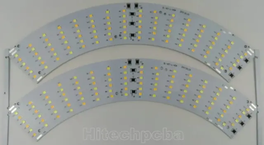
LED PCB Assembly
What is the LED Circuit Board assembly?
Generally, LED PCB assembly is considered to be a circuit board that has the LED components soldered to it. The LED is soldered to the printed circuit board and features a chip that creates the light as electrically connected. A thermal heat sink and a ceramic base are used to bond the chip. Not all the PCB products can be used in Led industry, as an LED PCB is easy to create a high volume of heat, but making it hard to cool with traditional methods. For this reason, metal core PCB is widely used in LED application because of their enhanced ability to dissipate heat, especially aluminum pcb is often used to fabricate PCB for LED lights.
We’ve had great LED PCB assembly experiences with top LED chips to brand such as Cree, Luxeon, Osram, Nichia, Lumileds, MLS, EVERLIGHT, Samsung, LG, Seoul., etc. PCB LED lights can be incorporated into numerous lighting applications due to their combination of excellent energy efficiency, low cost and maximum design flexibility.

Application of LED PCB Assembly
Hitechpcba serves customers in different industries, providing highly reliable and innovative LED PCBs for various applications:
• Horticulture light LED PCB Assembly
• LED controller PCB Assembly
• Computer LED display and indicators
• LED lights PCB Assembly for medical use
• Automotive LED PCBs Assembly include PCBs for brake lights and headlights
• Street lighting LED PCB Assembly
• Flashlights and camping accessories
• Traffic light PCB Assembly
• Commercial lighting LED PCB Assembly
LED PCB Assembly specification
Number of layers for LED PCB
These layers are made up of aluminum and magnesium, but now have Copper base material and Ceramic base materials for LED PCB industry, we can meet it.
Aluminum LED PCBs stand out among other PCBs because it has a good insulation characteristic and has a better machinery performance, the cheap cost is one important factor too.
Types of layers for LED PCB Assembly
Normally, the base layer is made using aluminum alloy metal.
This aluminum alloy substrate used in making the base makes it ideal for through-hole technology which transfers and dissipates heat.
A thermal insulation layer is made using some ceramic polymer which has good viscoelasticity characteristics.
It is highly heat resistant and protects the PCB against heat and mechanical stress.
The circuit layer, which is covered by a copper foil which can range from one to ten ounces.
LED Board type- single or in panel
Some boards are shapeless. For this reason, LED PCB panels are used. This reduces time, labor production and testing time.
Some LED PCB Assembly is done on a single board while others are done on panel boards.
LED PCB Assembly Process
Roughly, the PCBA process can be divided into theses phases: soldering paste printing > SMT (surface mounted technology) > reflow soldering > AOI (automated optical inspection)> THT (through-hole technology) > wave soldering > touch-up and cleaning > IC-programming > FCT (functional tests) > aging testing.
Below we show you the process.
Step1. Summarizing Project Information
Before contacting your supplier, make sure you have all the project information. Suppliers will need info following for quoting LED PCB assembly:
Gerber
BOM
LED PCB specification
Quotation quantity
Once you have gathered these information, you can contact us and request for a quote.
Of course, you can also provide the schematic, LED PCB Assembly pictures and even samples to us. The more details they have, the more accurate the supplier’s quotation will be.
Step2. Discussion and details about custom LED PCB Assembly
Different projects will have different requirements. Remember the special requirements mentioned in step 1? That’s going to be the focus of this session. Equipment and engineering capacity will not be identical between suppliers. Make sure your supplier has the equipment to produce and assemble major components and the corresponding testing capabilities.
For example, some vendors don’t have X-ray testing equipment, which means they can’t check the mount quality of BGA chips. Outsourcing this step will increase risk and cost. That’s what you don’t want.
Also, pay attention to time taken by the supplier to quote. Motherboards often contain hundreds or even thousands of components, and they are supplied by different manufacturers. To ensure the quality of the components, the supplier sourcing team will make multi-inquiries from these manufacturers or authorized suppliers to match customer’s requirement, which usually takes 2-3 business days, and even longer for some scarce chips. Therefore, if your project is complex and the supplier quotes you within few hours, double check with them.
Step3. Sample and feedback
After confirming the PI, the supplier will usually provide pre-production samples for your approval. At the same time, the supplier will also confirm with you the logistics plan of the bulk goods. Make sure they understand your shipping requirements, including details on packaging, customs clearance, taxes, etc.
For us to have a successful LED PCB Assembly process, its functions must be defined. Compliance requirement is defined to reduce the effect when components are selected.
The Bill of Materials is then generated from the information installed on the LED PCB.
All this information is used to assemble components which are identified from MOB to the LED PCB.
After that, the routing of traces is determined to each component, based on the size, shape of the circuit board and location of connectors.

Hitech Circuits is trusted by thousands of electronic engineers on their LED PCB assembly projects, from consumer, led bulb to precisely medical LED light, we can help you from the beginning of design stage; From commercial flood LED to industrial high power LED, from automotive LED to military LED, Venture is the perfect place for your LED PCB assembly requirement.
Hitech Circuits has been participated in hundreds and thousands of LED lighting projects, by providing LED PCB and also LED PCB assembly service.
Our LED PCB assembly had covered both ends of the Lighting Class LED size spectrum, assembling some of the largest (2 meter long boards) and some of the smallest LED Lighting applications which used in Medical Endoscopes.
LED PCB Assembly is very crucial in the current industrial development. Many electrical devises are being innovated and the old once being improved.
LED PCBs are useful due to the fact that they are made using materials that can transfer and dissipate heat. This characteristic increases device durability.
The world is changing with new technology, especially PCB technology that plays an essential role in the application of LED circuits. And the LED industry is taking advantage of this technology and growing faster.
As a full feature PCB solutions provider with more than a decade of experience, we're capable to provide LED PCB fabrication, components procurement and LED PCB assembly all under one roof. We can work with you to develop metal core PCB, aluminum circuit boards customized to your specific applications. We feature competitively priced PCBs made with standard FR-4 material that includes a thermal aluminum clad layer that will efficiently dissipate heat, keep all LED PCB components cool and significantly enhance the performance of your products.

LED pcb board, LED pcb assembly
LED with its advantages of high brightness, high efficiency, low heat, long life, is considered the most development potential in the 21st century lighting. In the market and policy driven by the rapid development of the domestic LED industry blowout has formed a relatively complete industrial chain, including the production of epitaxial wafers, chip preparation, packaging, integration, LED application. In 2010, China's LED industry scale, up from $ 827 billion in 2019 to 220 billion yuan, an annual growth rate of over 70%, higher than the 50% level of growth of the global LED lighting industry output value. Among them, the middle and lower reaches of the most complete industrial chain, accounting for 90% of the overall percentage of the GDP.Chinahas become the world's leading LED manufacturing base and important application market.
To further promote the technological innovation of the LED industry, construction and wide application of independent industry chain, China Electronic Appliance Corporation and industry associations to organize the theme of "Focus on the core energy LED Exhibition will be held November 9-11, 2010 in Shanghai International Expo Center and the 78th China Electronics Fair over the same period will be held will create from raw materials, epitaxial wafers, chip, LED bracket, LED accessories, LED packaging and supporting materials, the LED backlight upstream firm to the upstream and downstream enterprises of the display, lighting, landscaping, decorative lighting, traffic lights, automotive lighting, special lighting, to the equipment, instrumentation, software, finance, consulting and other service enterprises and technological exchanges and market trading platform, help the domestic industry sustained and healthy development, and promote the steady expansion of the LED application market.
In the LED industry chain upstream of the epitaxial wafers and LED chips accounted for 70% of the profits of the whole industry, and technology-intensive, capital-intensive, where the core technology of the LED. Well-known epitaxial wafer and chip production enterprises will be exhibited a number of energy-efficient, low heat, cost-effective LED products, many of whom have excellent products of international advanced level.
LED electronic pcb assembly manufacturing 100% Original LED Chip with one-stop in-house pcba services
3 notes
·
View notes
Text
Global Industrial Control Printed Circuit Board (PCB) Market: Growth Trends, Opportunities, and Forecast 2025–2032
MARKET INSIGHTS
The global Industrial Control Printed Circuit Board Market size was valued at US$ 3.21 billion in 2024 and is projected to reach US$ 5.34 billion by 2032, at a CAGR of 7.6% during the forecast period 2025-2032. The U.S. market accounts for 28% of global revenue, while China’s market is growing at a faster pace with an estimated 9.1% CAGR through 2032.
Industrial Control PCBs are specialized circuit boards designed for harsh industrial environments, featuring enhanced durability, thermal stability, and signal integrity. These boards form the backbone of automation systems, powering applications ranging from motor controls to robotics. Key product segments include Phenolic Resin PCBs (projected to reach USD 890 million by 2032), Fiberglass PCBs, and high-performance Polyimide PCBs for extreme temperature applications.
Market growth is driven by Industry 4.0 adoption, with industrial automation investments reaching USD 326 billion globally in 2023. Major players like Nippon Mektron and Sumitomo Electric dominate the supply chain, collectively holding over 35% market share. Recent developments include MEIKO Electronics’ 2024 expansion of high-mix PCB production capacity in Vietnam to address growing Southeast Asian demand.
MARKET DYNAMICS
MARKET DRIVERS
Rising Industrial Automation Investments to Fuel PCB Demand Across Manufacturing Sectors
The global push toward industrial automation is significantly boosting demand for industrial control PCBs. Manufacturing facilities are increasingly adopting automated systems requiring robust circuit boards for motor controls, robotics, and process automation equipment. Recent data indicates over 35% of manufacturing plants now utilize some form of industrial automation, with Asia-Pacific leading adoption at 42% penetration. These automation systems rely on specialized PCBs capable of withstanding harsh industrial environments while maintaining precise signal integrity. The growing emphasis on predictive maintenance and IoT-enabled equipment further accelerates PCB integration into industrial control systems.
Expansion of Renewable Energy Infrastructure Driving High-Power PCB Requirements
Renewable energy projects are creating substantial demand for industrial-grade PCBs capable of handling high voltage applications. Solar inverters, wind turbine control systems, and power converters all require specialized circuit boards with superior thermal management and durability. The renewable energy sector is projected to grow at nearly 9% CAGR through 2030, directly correlating to increased PCB requirements. These applications demand boards with specialized materials like polyimide or ceramic substrates to endure extreme temperature fluctuations and outdoor conditions. Recent technological breakthroughs in conductive materials have enabled PCBs to handle voltages exceeding 2kV while maintaining compact form factors.
Additionally, grid modernization initiatives are prompting utilities to upgrade substation automation systems, creating new opportunities for industrial control PCB manufacturers.
➤ For instance, multiple countries have announced plans to replace aging grid infrastructure, with projected investments exceeding $500 billion globally through 2030.
Furthermore, the proliferation of electric vehicle charging stations represents another growth vector, as these installations require rugged PCBs for power conversion and load management systems.
MARKET RESTRAINTS
Supply Chain Fragility Creating Component Shortages and Pricing Volatility
The industrial PCB market continues facing significant supply chain constraints affecting raw material availability and lead times. Copper foil prices have fluctuated nearly 40% annually in recent years, while epoxy resin supplies remain inconsistent due to geopolitical factors and production capacity limitations. These disruptions create unpredictable manufacturing costs that many smaller PCB producers struggle to absorb. Approximately 68% of surveyed manufacturers report experiencing at least one critical component shortage per quarter, forcing design compromises or production delays. The specialized nature of industrial-grade materials exacerbates these challenges, as alternative sourcing options are often limited.
Other Restraints
Technical Certification Bottlenecks Industrial PCBs must meet stringent certifications (UL, IPC Class 4, etc.) that require extensive testing protocols. The certification process often takes 12-18 months for new board designs, delaying time-to-market for control system manufacturers. These regulatory hurdles are particularly challenging for small and medium OEMs attempting to enter specialized industrial segments.
Labor Intensive Process Requirements Industrial PCB fabrication involves complex multilayer constructions requiring experienced technicians. The industry faces a growing skills gap, with 42% of manufacturers reporting difficulty finding qualified personnel for high-mix production environments. This shortage limits production scalability during periods of peak demand.
MARKET CHALLENGES
Miniaturization Demands Collide With Industrial Durability Requirements
Industrial equipment manufacturers increasingly demand smaller PCBs with higher component density, creating engineering paradoxes for circuit board producers. While consumer electronics can adopt flexible PCBs and advanced packaging, industrial applications require robust constructions resistant to vibration, moisture and electromagnetic interference. This tension between miniaturization and ruggedization forces difficult design compromises. Testing data shows industrial PCBs experience 40% higher failure rates when attempting ultra-high-density designs compared to conventional layouts. The challenge intensifies for high-power applications where thermal dissipation requirements conflict with space constraints.
Other Challenges
Lead Time Compression Pressures Industrial customers now expect 6-8 week lead times matching commercial PCB delivery standards, despite industrial boards requiring more complex manufacturing processes. This compression creates quality control risks as manufacturers attempt to accelerate production without compromising reliability testing protocols.
Counterfeit Component Risks The industrial PCB sector faces growing issues with counterfeit electronic components, particularly for legacy systems requiring obsolete parts. Recent industry audits found 12% of industrial PCB assemblies contained at least one counterfeit or remarked component, posing reliability concerns for critical infrastructure applications.
MARKET OPPORTUNITIES
Emerging Direct Metal Laser Sintering Technologies Enabling Novel PCB Architectures
Additive manufacturing techniques are creating breakthrough opportunities for industrial PCB designs. Advanced 3D printing methods now allow direct metal deposition onto dielectric substrates, enabling embedded components and unconventional board geometries. This proves particularly valuable for industrial applications requiring non-planar board configurations or integrated thermal management features. Early adopters report 30% space savings and 25% weight reduction compared to traditional PCB constructions while maintaining industrial durability standards. The technology also facilitates rapid prototyping capabilities previously unavailable for multilayer industrial boards.
Moreover, developments in embedded component technology allow industrial PCB manufacturers to incorporate passives and even some ICs directly into board layers. This innovation enhances reliability by eliminating solder joints while enabling more compact form factors.
➤ Select manufacturers have already demonstrated boards with 50+ embedded components maintaining IPC Class 3 reliability standards.
Additionally, advancements in optical PCB interconnects present new possibilities for industrial environments with intense electromagnetic interference. These photonic circuits show particular promise for factory automation systems and power generation equipment where electrical noise traditionally limits performance.
INDUSTRIAL CONTROL PRINTED CIRCUIT BOARD MARKET TRENDS
Growing Automation in Industrial Sectors to Drive Market Expansion
The global industrial control printed circuit board (PCB) market is experiencing significant growth, primarily driven by increasing automation across manufacturing, energy, and transportation sectors. The shift towards Industry 4.0 has led to higher demand for complex PCB solutions that support smart factories, robotics, and IoT-enabled industrial control systems. Analysts estimate that the market, valued at millions in 2024, will witness a steady CAGR over the forecast period due to this automation wave. High-speed, multi-layer PCBs with enhanced thermal management are particularly in demand as industrial systems require more sophisticated control mechanisms. Furthermore, as factories upgrade legacy systems to incorporate AI-driven quality control and predictive maintenance, PCB manufacturers are responding with designs that emphasize reliability under harsh industrial conditions.
Other Trends
Adoption of High-Performance Substrates
The industrial control PCB market is seeing increased adoption of advanced substrate materials such as polyimide and high-frequency laminates. These materials offer superior thermal stability and signal integrity compared to traditional epoxy boards, making them indispensable in high-power industrial applications. The phenolic resin PCB segment, though established, is facing competition from these emerging alternatives as manufacturers prioritize durability in extreme environments. Recent innovations include embedded component PCBs, which reduce failure points by integrating passive components directly into the board structure—a critical advantage for industrial control systems where downtime is costly.
Regional Manufacturing Shifts Impacting Supply Chains
While China remains the dominant producer, accounting for a substantial share of global industrial control PCB output, geopolitical factors are prompting manufacturers to diversify production locations. Southeast Asia and North America are emerging as alternative hubs, with several key players establishing facilities in these regions. The U.S. market, though smaller in volume compared to China, commands premium pricing for specialized industrial PCBs used in defense and aerospace applications. Additionally, sustainability concerns are driving innovation in board manufacturing processes, with lead-free soldering and halogen-free laminates gaining traction among environmentally conscious industrial customers. This shift is reshaping traditional supply chain dynamics across the sector.
COMPETITIVE LANDSCAPE
Key Industry Players
Market Leaders Pursue Innovation and Global Expansion to Maintain Dominance
The industrial control PCB market features a diverse mix of established multinationals and regional specialists competing across different application segments. MEIKO Electronics Co., Ltd. and Nippon Mektron, Ltd. emerged as dominant players in 2024, collectively accounting for nearly 18% of global revenue share. Their leadership stems from vertically integrated manufacturing capabilities and strong partnerships with industrial automation providers.
Sumitomo Electric Industries has gained significant traction through its high-reliability PCB solutions for harsh industrial environments, while German manufacturer AT&S continues to expand its market position through technological innovations in multilayer PCBs. The Asia-Pacific region, particularly China and Japan, houses several fast-growing competitors including Shengyi Technology and Victory Giant Technology, who are capitalizing on localized supply chains and cost advantages.
Recent strategic movements include Würth Elektronik‘s acquisition of a Turkish PCB manufacturer to strengthen its EMEA presence, and Amphenol‘s $120 million investment in advanced manufacturing facilities. Such developments indicate the industry’s focus on both technological advancement and geographical diversification to serve global industrial automation demands.
List of Key Industrial Control PCB Manufacturers
MEIKO Electronics Co., Ltd. (Japan)
Nippon Mektron, Ltd. (Japan)
Sumitomo Electric Industries, Ltd. (Japan)
Würth Elektronik (Germany)
GulTech (Singapore)
AT&S (Austria)
Amphenol (U.S.)
Summit Interconnect (U.S.)
STEMCO (South Korea)
BHFlex (South Korea)
Victory Giant Technology (China)
Shengyi Technology Co.,Ltd (China)
Aoshikang Technology Co.,Ltd (China)
Daeduck Group (South Korea)
Segment Analysis:
By Type
Fiberglass Printed Circuit Board Segment Dominates Due to Superior Durability and Thermal Resistance
The market is segmented based on type into:
Phenolic Resin Printed Circuit Board
Subtypes: Standard phenolic, high-temperature phenolic
Fiberglass Printed Circuit Board
Polyimide Printed Circuit Board
Subtypes: Flexible polyimide, rigid polyimide
Epoxy Resin Printed Circuit Board
By Application
Industrial Power Segment Leads Due to Growing Automation in Manufacturing Facilities
The market is segmented based on application into:
Server
Industrial Power
Industrial Manipulator
By Layer Count
Multilayer PCBs Gain Traction for Complex Industrial Control Systems
The market is segmented based on layer count into:
Single-layer PCB
Double-layer PCB
Multilayer PCB
By End-Use Industry
Manufacturing Sector Emerges as Key Consumer Due to Industry 4.0 Adoption
The market is segmented based on end-use industry into:
Automotive
Manufacturing
Energy & Power
Telecommunications
Regional Analysis: Industrial Control Printed Circuit Board Market
North America North America remains a critical hub for industrial control PCB manufacturing, driven by advanced automation adoption and robust Industry 4.0 investments. The U.S. dominates the regional market, accounting for over 70% of demand, with key applications in industrial power systems and server infrastructure. However, the region faces challenges from supply chain disruptions and labor shortages, which have pushed manufacturers to diversify sourcing strategies. A notable trend is the shift toward high-density interconnect (HDI) PCBs, particularly for smart factory applications. The US CHIPS and Science Act has further accelerated domestic PCB production, reducing reliance on imports.
Europe Europe’s market is characterized by stringent EU RoHS compliance and a strong emphasis on sustainable PCB manufacturing. Germany leads with innovations in automotive-grade PCBs for industrial robotics, while France focuses on energy-efficient designs for smart grids. The Russia-Ukraine conflict has impacted raw material availability, forcing manufacturers to adopt alternative substrate materials like polyimide. European PCB suppliers are increasingly collaborating with local industrial automation firms to shorten lead times. Despite economic headwinds, miniaturization trends and IoT integration are driving steady demand for multi-layer PCBs.
Asia-Pacific As the largest production base, APAC commands over 60% of global PCB output, with China’s Shenzhen cluster serving as the industry epicenter. While labor cost advantages persist, rising wages are pushing manufacturers toward automated production lines. India is emerging as an alternative manufacturing destination, particularly for low-to-mid range PCBs, though quality consistency remains a challenge. The region faces overcapacity risks in standard PCBs but shows strong potential in high-frequency boards for 5G-enabled industrial controls. Japan retains leadership in high-reliability PCBs for precision equipment, leveraging decades of materials science expertise.
South America The region presents a nascent but growing opportunity, with Brazil accounting for nearly 50% of regional PCB demand. Local production is constrained by limited technical expertise and import dependence, compelling industrial firms to source from Asia. Recent trade agreements have improved access to Chinese-made PCBs, though infrastructure gaps hinder just-in-time delivery. Mining and oil/gas sectors drive demand for ruggedized circuit boards, while currency volatility complicates long-term planning. Some countries are offering tax incentives to attract PCB assembly plants, but progress remains slow.
Middle East & Africa MEA’s market is bifurcated into Gulf Cooperation Council (GCC) technology adopters and African emerging markets. The UAE and Saudi Arabia are investing heavily in industrial automation PCBs for smart city projects, relying primarily on European and Asian imports. South Africa maintains limited PCB assembly capabilities for mining equipment controls, while North African nations serve as low-cost assembly hubs for European firms. The region faces logistics bottlenecks and lacks domestic raw material suppliers, but economic diversification policies are gradually improving market access.
Report Scope
This market research report provides a comprehensive analysis of the global and regional Industrial Control Printed Circuit Board (PCB) markets, covering the forecast period 2025–2032. It offers detailed insights into market dynamics, technological advancements, competitive landscape, and key trends shaping the industry.
Key focus areas of the report include:
Market Size & Forecast: Historical data and future projections for revenue, unit shipments (K Sqm), and market value across major regions and segments. The Global Industrial Control PCB market was valued at USD million in 2024 and is projected to reach USD million by 2032.
Segmentation Analysis: Detailed breakdown by product type (Phenolic Resin, Fiberglass, Polyimide, Epoxy Resin PCBs), application (Server, Industrial Power, Industrial Manipulator), and end-user industry to identify high-growth segments.
Regional Outlook: Insights into market performance across North America, Europe, Asia-Pacific, Latin America, and Middle East & Africa, including country-level analysis. The U.S. market is estimated at USD million in 2024, while China is projected to reach USD million.
Competitive Landscape: Profiles of leading manufacturers including MEIKO Electronics, Nippon Mektron, Sumitomo Electric, Wurth, AT&S, and Amphenol, covering their market share, product portfolios, and strategic developments.
Technology Trends & Innovation: Assessment of emerging PCB technologies, integration with Industry 4.0 systems, material advancements, and evolving manufacturing standards.
Market Drivers & Restraints: Evaluation of industrial automation growth, smart manufacturing adoption, supply chain challenges, and raw material price volatility.
Stakeholder Analysis: Strategic insights for PCB manufacturers, industrial equipment OEMs, component suppliers, and investors regarding market opportunities.
Related Reports:
https://semiconductorblogs21.blogspot.com/2025/06/global-pecvd-equipment-market-size.htmlhttps://semiconductorblogs21.blogspot.com/2025/06/global-embedded-sbc-market-trends-and.htmlhttps://semiconductorblogs21.blogspot.com/2025/06/global-encoder-chips-market-driving.htmlhttps://semiconductorblogs21.blogspot.com/2025/06/global-bluetooth-audio-chips-and.htmlhttps://semiconductorblogs21.blogspot.com/2025/06/semiconductor-ip-blocks-market-growth.htmlhttps://semiconductorblogs21.blogspot.com/2025/06/global-dc-power-supply-for.htmlhttps://semiconductorblogs21.blogspot.com/2025/06/global-high-voltage-power-supply-for.htmlhttps://semiconductorblogs21.blogspot.com/2025/06/global-industrial-sun-sensors-market.htmlhttps://semiconductorblogs21.blogspot.com/2025/06/global-consumer-grade-contact-image.htmlhttps://semiconductorblogs21.blogspot.com/2025/06/global-non-residential-occupancy.htmlhttps://semiconductorblogs21.blogspot.com/2025/06/global-standalone-digital-signage.htmlhttps://semiconductorblogs21.blogspot.com/2025/06/12-inch-silicon-wafers-market-global-12.htmlhttps://semiconductorblogs21.blogspot.com/2025/06/global-12-inch-semiconductor-silicon.htmlhttps://semiconductorblogs21.blogspot.com/2025/06/global-extreme-ultraviolet-lithography.htmlhttps://semiconductorblogs21.blogspot.com/2025/06/global-industrial-touchscreen-market.htmlhttps://semiconductorblogs21.blogspot.com/2025/06/global-distributed-fiber-optic-sensor.html
0 notes
Text
Antenna in Package AiP Market Opportunities Rising with Expansion of Millimeter Wave Technology Globally
The Antenna in Package (AiP) market is gaining significant traction as wireless communication technologies become increasingly integrated into compact, high-performance electronic devices. AiP technology incorporates antennas directly into semiconductor packages, enabling advanced radio frequency (RF) performance while saving space. This innovation is particularly relevant in 5G, millimeter-wave (mmWave), automotive radar, satellite communications, and IoT applications.

Market Drivers
One of the primary drivers of the AiP market is the global rollout of 5G technology, which operates at higher frequencies such as mmWave. These frequencies require advanced antenna solutions capable of handling high data rates and low latency. Traditional printed circuit board (PCB) antennas often fall short in terms of integration and performance. AiP offers a more efficient alternative by reducing interconnect losses and supporting beamforming technologies critical for 5G.
Another major factor is the increasing miniaturization of consumer electronics. Smartphones, wearables, and IoT devices demand compact components that deliver excellent performance. AiP technology meets this requirement by integrating the antenna and RF front-end into a single compact module, freeing up space and improving system-level efficiency.
Technological Advancements
Recent advancements in substrate materials, system-in-package (SiP) technologies, and 3D packaging are making AiP solutions more cost-effective and scalable. Low-temperature co-fired ceramic (LTCC) and organic substrates have enabled better thermal and electrical performance. Integration of multiple functions such as filters, power amplifiers, and transceivers within the package has allowed manufacturers to create multi-functional modules tailored for specific end-uses.
In addition, the evolution of advanced simulation tools and design automation has shortened development cycles and reduced costs, making AiP more accessible to a broader range of industries. These advancements have facilitated faster prototyping and more reliable testing environments.
Key Market Segments
The AiP market can be segmented based on frequency band, end-user application, and geography.
By frequency, the market includes sub-6 GHz and mmWave segments, with mmWave seeing higher growth due to its necessity in 5G and automotive radar applications.
By application, the market is divided into consumer electronics, automotive, telecommunications, aerospace and defense, and industrial IoT.
Geographically, North America and Asia-Pacific dominate the AiP landscape, thanks to the presence of major semiconductor companies and 5G infrastructure deployment.
Regional Insights
Asia-Pacific leads the AiP market due to robust electronics manufacturing ecosystems in countries like China, South Korea, Taiwan, and Japan. Government initiatives to boost 5G and smart city projects further support AiP growth in the region. North America, especially the United States, sees significant demand from telecom providers, defense contractors, and autonomous vehicle manufacturers. Europe is also emerging as a key region, driven by automotive and industrial automation applications.
Competitive Landscape
The AiP market is highly competitive, with key players including Qualcomm, ASE Group, Amkor Technology, Murata Manufacturing, TSMC, and MediaTek. These companies are investing in research and development to improve integration, reduce power consumption, and enhance RF performance. Collaborations, joint ventures, and strategic acquisitions are common strategies to gain market share and accelerate product development.
Startups and mid-sized players are also entering the space with niche AiP solutions for IoT and wearable devices, contributing to market dynamism and innovation.
Challenges and Opportunities
Despite its promise, AiP adoption faces several challenges. High design complexity, thermal management issues, and initial manufacturing costs are significant barriers. Additionally, maintaining signal integrity in densely packed modules remains a technical hurdle.
However, opportunities abound. As mmWave adoption expands and edge computing grows in importance, AiP is poised to play a pivotal role in enabling low-latency, high-speed communication across various devices and systems. The trend toward smart cities, connected vehicles, and AR/VR applications also offers long-term growth potential.
Future Outlook
The AiP market is expected to grow at a CAGR exceeding 15% over the next five years, driven by surging demand across multiple industries. Technological advancements, cost optimization, and expanding 5G infrastructure will be key enablers. As device manufacturers strive to balance performance, size, and power efficiency, AiP is likely to become a standard in RF design and packaging.
#AntennaInPackage#AiPMarket#5GTechnology#MillimeterWave#WirelessCommunication#IoTDevices#RFTechnology
0 notes
Text
Printed Circuit Board Market Future Trends: Emerging Technologies and Growth Opportunities Driving Innovation
The printed circuit board market is witnessing significant transformation as innovation and technological advancements propel its growth. PCBs, the backbone of modern electronic devices, continue to evolve in response to emerging industry needs, consumer demands, and new applications. Understanding the future trends shaping the PCB market is essential for manufacturers, investors, and technology enthusiasts seeking to capitalize on opportunities and anticipate challenges.

One of the foremost trends in the PCB market is the increasing demand for miniaturization. As electronic devices become more compact and multifunctional, the need for smaller, lighter, and more efficient PCBs has intensified. This trend is especially prominent in sectors like consumer electronics, healthcare, and automotive, where space constraints and performance requirements drive innovation. Flexible PCBs and rigid-flex boards are gaining popularity as they allow intricate designs that fit into compact devices without compromising functionality.
Advanced materials are another crucial factor shaping the PCB market’s future. The traditional use of fiberglass and epoxy resins is gradually being supplemented or replaced by high-performance substrates such as polyimide, ceramic, and Teflon. These materials offer superior thermal stability, electrical performance, and mechanical strength, which are critical for high-frequency and high-speed applications. This shift supports the growing demands of 5G technology, aerospace, and military electronics where reliability under extreme conditions is vital.
The rise of 5G technology is a major catalyst driving the evolution of PCBs. The implementation of 5G networks requires PCBs that can handle high-frequency signals with minimal interference and signal loss. This has led to innovations in high-density interconnect (HDI) PCBs, which allow more components to be packed into a smaller area with enhanced electrical performance. The demand for HDI PCBs is expected to surge as 5G infrastructure expands globally, impacting telecommunications, IoT devices, and smart cities.
Sustainability and environmental concerns are increasingly influencing the PCB market’s future. The electronics industry is under pressure to reduce its environmental footprint, leading to the development of eco-friendly PCB manufacturing processes and materials. Lead-free soldering, recyclable substrates, and reduced hazardous chemical use are becoming standard practices. Companies that embrace green manufacturing are likely to gain competitive advantages as consumers and regulators prioritize sustainability.
Automation and Industry 4.0 integration are revolutionizing PCB manufacturing. The adoption of artificial intelligence (AI), robotics, and machine learning in production lines improves precision, reduces defects, and accelerates manufacturing cycles. Automated optical inspection (AOI) systems and real-time monitoring help maintain high-quality standards while reducing costs. This trend not only boosts efficiency but also allows manufacturers to respond swiftly to customized and small-batch orders, which are increasingly common due to diversified product demands.
The automotive industry continues to be a major driver of PCB market growth, especially with the rise of electric vehicles (EVs) and autonomous driving technology. PCBs in EVs must withstand higher temperatures and voltages while maintaining safety and durability. Advanced PCBs facilitate battery management systems, power electronics, and sensor integration crucial for EV performance. Additionally, autonomous vehicles rely heavily on sophisticated sensor arrays and computing power, all of which depend on innovative PCB designs.
Healthcare technology is another promising sector influencing PCB trends. The surge in wearable medical devices, telehealth solutions, and diagnostic equipment requires PCBs that offer reliability, miniaturization, and biocompatibility. Flexible PCBs enable comfortable and accurate wearable sensors, while multilayer PCBs support complex diagnostic devices. The ongoing digitalization of healthcare creates a continuous demand for cutting-edge PCB solutions tailored to medical applications.
Global supply chain dynamics also impact the PCB market’s future. The COVID-19 pandemic exposed vulnerabilities in electronics supply chains, prompting companies to rethink sourcing and manufacturing strategies. There is a noticeable trend toward regionalization and diversification to minimize risks and reduce lead times. This shift may result in increased investments in local PCB manufacturing capabilities, encouraging innovation and customization closer to end markets.
Another important future trend is the increasing use of embedded components within PCBs. Embedding passive and active components directly into the PCB substrate reduces assembly time, improves reliability, and enables higher circuit density. This technology is particularly valuable in compact and high-performance devices such as smartphones, tablets, and aerospace electronics, where every millimeter of space counts.
Lastly, the integration of PCBs with emerging technologies such as augmented reality (AR), virtual reality (VR), and artificial intelligence (AI) will open new growth avenues. These technologies demand highly complex, lightweight, and reliable PCBs to support sensors, processors, and communication modules. As these applications gain traction across entertainment, education, and industrial sectors, PCB manufacturers will need to innovate to meet their unique requirements.
In conclusion, the printed circuit board market is poised for dynamic growth fueled by miniaturization, advanced materials, 5G adoption, sustainability initiatives, and Industry 4.0 automation. Key industries such as automotive, healthcare, and telecommunications will continue to drive demand for innovative PCB solutions. Manufacturers who embrace emerging technologies, invest in eco-friendly processes, and adapt to shifting supply chain models will be best positioned to thrive. As the market evolves, staying informed about these future trends will be essential for all stakeholders navigating the complex landscape of PCB technology.
0 notes
Text
PCB Materials: A Comprehensive Guide to Choosing the Right Substrates

Printed Circuit Boards (PCBs) are the backbone of modern electronics, providing the foundation for electrical connections between components. The performance, durability, and reliability of a PCB heavily depend on the PCB materials used in its construction. Selecting the right substrate is crucial for ensuring optimal functionality in various applications, from consumer electronics to aerospace systems.
This guide explores the different types of PCB materials, their properties, and how to choose the best option for your project.
1. Understanding PCB Materials: Key Properties
PCB materials consist of a substrate (base layer) and conductive traces (usually copper). The substrate must provide mechanical support while maintaining electrical insulation. The most important properties to consider when selecting PCB materials include:
Dielectric Constant (Dk): Determines signal propagation speed; lower Dk is better for high-frequency applications.
Dissipation Factor (Df): Measures signal loss; a low Df is essential for high-speed circuits.
Thermal Conductivity: Affects heat dissipation; critical for high-power applications.
Coefficient of Thermal Expansion (CTE): Must match component materials to avoid warping under temperature changes.
Glass Transition Temperature (Tg): The temperature at which the substrate softens; higher Tg improves thermal stability.
2. Common Types of PCB Materials
Different applications require different PCB materials. Below are the most widely used substrates:
2.1 FR-4 (Flame Retardant-4)
FR-4 is the most common PCB material, made from woven fiberglass and epoxy resin. It offers good mechanical strength, electrical insulation, and affordability.
Advantages:
Cost-effective
Good mechanical and electrical properties
Suitable for most standard applications
Limitations:
Moderate thermal performance
Not ideal for high-frequency or high-power circuits
2.2 High-Frequency Laminates
For RF and microwave applications, specialized PCB materials like Rogers, PTFE (Teflon), and ceramic-filled substrates are used.
Examples:
Rogers RO4000 Series: Low Dk and Df, ideal for 5G and radar systems.
PTFE (Teflon): Excellent high-frequency performance but harder to manufacture.
Advantages:
Minimal signal loss at high frequencies
Stable electrical properties
Limitations:
Higher cost
Requires specialized fabrication techniques
2.3 Metal-Core PCBs (MCPCBs)
MCPCBs use a metal base (usually aluminum or copper) for better heat dissipation.
Applications:
LED lighting
Power electronics
Automotive systems
Advantages:
Superior thermal management
Enhanced durability
Limitations:
Higher cost than FR-4
Heavier than standard PCBs
2.4 Flexible PCB Materials
Flexible PCBs use polyimide or polyester films instead of rigid substrates.
Advantages:
Lightweight and bendable
Suitable for wearable electronics and compact devices
Limitations:
More expensive than rigid PCBs
Requires careful handling during assembly
3. How to Choose the Right PCB Material
Selecting the best PCB materials depends on several factors:
3.1 Application Requirements
Consumer Electronics: FR-4 is usually sufficient.
High-Frequency Circuits: Rogers or PTFE laminates are better.
High-Temperature Environments: Polyimide or ceramic-based materials.
3.2 Signal Integrity Needs
For high-speed digital or RF designs, low Dk and Df materials are essential to minimize signal loss.
3.3 Thermal Management
Power electronics and LED applications require materials with high thermal conductivity, such as MCPCBs.
3.4 Cost Considerations
While advanced PCB materials offer superior performance, they are more expensive. Balance performance needs with budget constraints.
4. Future Trends in PCB Materials
As technology evolves, new PCB materials are being developed to meet higher performance demands:
High-Tg FR-4: Improved thermal stability for advanced computing.
Nanocomposite Substrates: Enhanced electrical and thermal properties.
Eco-Friendly Materials: Biodegradable and lead-free options for sustainable electronics.
Conclusion
Choosing the right PCB materials is critical for ensuring the performance, reliability, and longevity of electronic devices. By understanding the properties and applications of different substrates—such as FR-4, high-frequency laminates, metal-core, and flexible PCBs—engineers can make informed decisions based on their project requirements.
As emerging technologies demand faster, smaller, and more efficient PCBs, advancements in PCB materials will continue to play a vital role in shaping the future of electronics.
1 note
·
View note
Text
PCB Materials: A Comprehensive Guide to Choosing the Right Substrate

Printed Circuit Boards (PCBs) are the backbone of modern electronics, and selecting the right PCB materials is crucial for performance, durability, and cost-effectiveness. The substrate used in PCB manufacturing determines electrical properties, thermal resistance, and mechanical strength. This guide explores the different types of PCB materials, their properties, and how to choose the best one for your application.
1. Introduction to PCB Materials
PCB materials serve as the foundation for electronic circuits, providing insulation, support, and connectivity. The choice of material impacts signal integrity, heat dissipation, and overall reliability. Common PCB substrate materials include:
FR-4
Polyimide
PTFE (Teflon)
Ceramic-based substrates
Metal-core PCBs
Each material has unique characteristics suited for different applications, from consumer electronics to aerospace systems.
2. Common Types of PCB Substrate Materials
2.1 FR-4: The Standard PCB Material
FR-4 is the most widely used PCB material, made from woven fiberglass cloth with an epoxy resin binder. It is flame-resistant (hence "FR") and offers good mechanical and electrical properties.
Key Properties:
Cost-effective
Moderate thermal resistance (~130°C)
Good electrical insulation
Suitable for most consumer electronics
Applications:
Motherboards
LED lighting
Automotive control systems
2.2 Polyimide: High-Temperature Resistance
Polyimide is a high-performance PCB material known for its flexibility and thermal stability.
Key Properties:
Withstands extreme temperatures (up to 260°C)
Excellent chemical resistance
Flexible, making it ideal for bendable circuits
Applications:
Aerospace and military electronics
Medical devices
Wearable technology
2.3 PTFE (Teflon): High-Frequency Applications
PTFE (Polytetrafluoroethylene) is a premium PCB material used in high-frequency and RF applications due to its low dielectric loss.
Key Properties:
Ultra-low dielectric constant (~2.1)
Minimal signal loss at high frequencies
High thermal stability
Applications:
5G communication devices
Radar systems
Satellite technology
2.4 Ceramic-Based Substrates: Superior Thermal Conductivity
Ceramic PCB materials, such as aluminum oxide (Al₂O₃) and aluminum nitride (AlN), are used in high-power applications.
Key Properties:
Excellent thermal conductivity
High mechanical strength
Resistant to harsh environments
Applications:
Power electronics
LED modules
Automotive power systems
2.5 Metal-Core PCBs: Enhanced Heat Dissipation
Metal-core PCBs (MCPCBs) use aluminum or copper as the base layer for superior heat dissipation.
Key Properties:
High thermal conductivity
Improved durability
Better heat management than FR-4
Applications:
High-power LED systems
Power converters
Industrial motor controls
3. Factors to Consider When Choosing PCB Materials
3.1 Electrical Performance
Dielectric Constant (Dk): Affects signal speed; lower Dk is better for high-frequency PCBs.
Dissipation Factor (Df): Indicates signal loss; critical for RF applications.
3.2 Thermal Properties
Glass Transition Temperature (Tg): Higher Tg materials (e.g., polyimide) withstand more heat.
Thermal Conductivity: Important for power electronics to prevent overheating.
3.3 Mechanical Strength & Flexibility
Rigid PCBs (FR-4, ceramic) vs. flexible PCBs (polyimide).
Consider vibration resistance in automotive and aerospace applications.
3.4 Cost & Manufacturing Feasibility
FR-4 is the most economical, while PTFE and ceramic substrates are more expensive.
Some materials require specialized manufacturing processes.
4. Emerging Trends in PCB Materials
4.1 High-Speed Digital PCBs
With the rise of 5G and IoT, low-loss PCB materials like PTFE and modified epoxy resins are in demand.
4.2 Eco-Friendly PCB Substrates
Bio-based resins and halogen-free laminates are gaining popularity due to environmental regulations.
4.3 Advanced Thermal Management Solutions
New composite materials with embedded cooling channels are being developed for high-power electronics.
5. Conclusion
Choosing the right PCB materials is essential for optimizing performance, reliability, and cost. Whether you need high-frequency signal integrity (PTFE), extreme thermal resistance (polyimide), or cost-effective solutions (FR-4), understanding material properties ensures the best PCB design for your application.
By evaluating electrical, thermal, and mechanical requirements, engineers can select the ideal PCB substrate material for their projects, ensuring long-term durability and efficiency.
Would you like recommendations for a specific application? Let us know in the comments!
1 note
·
View note
Text
Viasion PCB: Your Trusted Partner for High-Quality Custom and Advanced PCBs
In today’s fast-paced electronics industry, choosing the right PCB manufacturer can make all the difference. Whether you're working on a new tech innovation or scaling an existing product, the quality, precision, and reliability of your printed circuit boards are critical. That’s where Viasion Technology Co., Ltd. steps in—a proven leader in the PCB industry with over 15 years of experience delivering excellence.
Viasion offers comprehensive PCB manufacturing and assembly services to clients across the globe, including the United States. From custom PCB boards to complex blind vias printed circuit boards, their products serve various industries including automotive, telecom, medical devices, and consumer electronics.
Why Choose Viasion for Your PCB Needs?
Viasion is more than just a custom PCB manufacturer. Their expertise spans across a wide range of advanced PCB types including blind via PCBs, ceramic PCBs, flexible PCBs, and copper based PCBs—all manufactured in ISO-certified facilities with stringent quality control.
Here’s a closer look at what makes Viasion a preferred partner:
1. Advanced Blind Via PCB Capabilities
For high-density interconnect (HDI) designs, blind vias PCBs are essential. These vias connect outer layers to inner layers without passing through the entire board, saving space and improving signal integrity. As a trusted blind vias PCB manufacturer, Viasion delivers precise, reliable blind via PCBs ideal for compact, high-speed devices.
Their expert team uses laser drilling and advanced lamination techniques to ensure accuracy and consistency in every board. Whether you're prototyping or in full-scale production, Viasion provides solutions that meet your specific requirements.
2. Durable and High-Performance Ceramic PCBs
When it comes to thermal conductivity, high-frequency performance, and durability, ceramic PCBs stand out. Ideal for aerospace, LED lighting, and automotive applications, these boards handle extreme environments where standard PCBs may fail.
As an experienced ceramic PCB manufacturer, Viasion offers a variety of ceramic substrates, including alumina and aluminum nitride, ensuring optimal performance even in the most demanding conditions. Their ceramic PCBs are designed to offer low thermal expansion, excellent insulation, and high mechanical strength.
3. Cost-Effective and Efficient Copper Based PCBs
Copper based PCBs are essential for high-power electronics due to their superior heat dissipation capabilities. These are commonly used in power converters, industrial control systems, and automotive components.
Viasion manufactures copper based PCBs with excellent reliability and durability. Their manufacturing process ensures a strong bond between copper and insulating layers, resulting in high-performance boards ready for tough applications.
4. Fully Customizable PCB Manufacturing
Need something tailored to your specific project? Viasion is a specialist custom PCB manufacturer, delivering bespoke PCB solutions that match your design and functional requirements. Whether it's a custom PCB board for a wearable device or a multi-layer board for an IoT product, their engineering team works closely with you to bring your design to life.
You’ll get DFM (Design for Manufacturing) support, fast prototyping, and competitive pricing—all while maintaining the highest quality standards.
5. Reliable Flexible PCB Manufacturing
For applications where space, weight, and flexibility are crucial, flexible PCBs are the go-to solution. Used in devices like smartphones, cameras, and medical instruments, flexible PCB boards allow for bendable, compact designs.
Viasion is a trusted flexible PCB manufacturer, producing single-sided, double-sided, and multi-layer flex PCBs. Their flex PCB capabilities include fine-line spacing, tight tolerances, and advanced materials like polyimide for high heat resistance.
Their flexible circuits are tested for bend cycles, ensuring longevity and reliability even under constant motion and mechanical stress.
Applications Across Every Industry
Viasion serves a wide array of industries:
Medical Devices: Miniaturized flexible PCBs and ceramic PCBs for diagnostic tools and implants
Automotive: High-temperature copper based PCBs and custom PCBs for control units
Consumer Electronics: High-density blind via PCBs and flexible PCBs for wearables and mobile devices
Telecommunications: Multi-layer custom PCBs and blind vias printed circuit boards for routers and servers
Industrial Equipment: Rugged ceramic PCBs and copper based PCBs for control systems
No matter your industry, Viasion brings the technical expertise and manufacturing excellence needed to make your project a success.
Why U.S. Customers Trust Viasion
Even though Viasion is based in Shenzhen, China, their services are perfectly aligned for U.S. businesses. With fast international shipping, English-speaking support staff, and a focus on total customer satisfaction, Viasion delivers a seamless experience for customers in the United States.
Key benefits for U.S. clients include:
No minimum order quantity
Quick turnaround and prototyping
Full turnkey PCB assembly service
Competitive pricing without compromising quality
UL and ISO certified production processes
Get Started Today
Whether you need a custom PCB board, ceramic PCB, or a complex blind vias PCB, Viasion is equipped to deliver top-tier solutions tailored to your unique specifications. Their dedication to quality, innovation, and customer support makes them the go-to custom PCB manufacturer for companies across the USA and beyond.
👉 Visit www.viasionpcb.com to request a quote or reach out to their team at [email protected] for personalized support.
0 notes
Text
BST Ceramic PCB: Your partner in Ceramic PCB solutions
In demanding electronic applications where performance is essential, traditional PCBs often fall short. That is where ceramic PCBs come in, offering a leap forward in reliability, thermal management, and overall efficiency.
At BST Ceramic PCB, we specialize in the manufacturing of high-performance ceramic circuit boards. Our advanced technology utilizes ceramic materials as the base for these PCBs, offering advantages over traditional FR-4 epoxy boards.
What sets ceramic PCBs apart?
Unlike conventional PCBs, ceramic core PCBs utilizes a ceramic base material, such as alumina or aluminium nitride. This ceramic substrate PCB construction brings a host of advantages:
Exceptional thermal conductivity: Dissipate heat rapidly and efficiently, even in high-power applications.
High-frequency performance: Ideal for applications requiring high signal speeds and minimal signal loss.
Dimensional Stability: Resistant to wrapping and shrinking, ensuring consistent performance in extreme environments.
Chemical resistance: Withstand harsh chemicals and environments, ensuring long-term reliability.
BST Ceramic PCB: Your partner in Ceramic PCB solutions
We offer a comprehensive range of ceramic base PCB solutions, including:
High temperature PCBs
High voltage PCBs
RF and Microwave PCBs
LED PCBs
Our team of experts will work closely with you to understand your unique requirements and deliver custom ceramic substrate PCBs that exceed your expectations.
Applications Across Industries
Our ceramic PCBs cater to a diverse range of industries due to their unique properties:
Telecommunications: Ideal for high-frequency applications like RF amplifies and microwave components.
Automotive: Withstand extreme temperatures and vibrations, making them perfect for engine control units and power electronics.
MedicalElectronics: Deliver reliable performance in demanding medical devices like pacemakers and defibrillators.
AerospaceandDefense: Function flawlessly in harsh environments for applications in satellites, radar systems, and military equipment.
Experience the BST Ceramic PCB Difference
Bestquality: We adhere to the highest industry standards to ensure superior product performance and reliability.
Cutting-EdgeTechnology: Our best facilities allow us to manufacture complex ceramic circuit boards with precision.
Customer-Centricapproach: We are committed to providing exceptional customer service and support throughout the entire process.
Contact us today to discuss your project requirements and experience the exceptional performance and reliability of BST Ceramic PCBs. Enhance your electronic devices to the next level with our latest technology.
0 notes
Text
CHIP Ceramic Patch Antenna vs. Bluetooth Patch Antenna: Which Is More Suitable for Your Device?
In wireless communication device design, antenna selection directly impacts signal transmission quality, device size, and user experience. With the rapid development of fields like the Internet of Things (IoT) and smart wearables, CHIP ceramic patch antennas and Bluetooth patch antennas have become mainstream choices due to their distinct characteristics.

I. Antenna Basics: CHIP Ceramic Patch Antenna vs. Bluetooth Patch Antenna
1. CHIP Ceramic Patch Antenna
Principle and Structure:Utilizes ceramic materials (such as dielectric ceramics) as the substrate, achieving signal transmission and reception through microstrip or radiation patch designs. The high dielectric constant of ceramics allows the antenna to operate at smaller sizes, suitable for high-frequency applications (e.g., 2.4GHz, 5GHz).
Core Advantages:
Multi-Band Compatibility: Supports Wi-Fi, Bluetooth, Zigbee, and other protocols, reducing the number of antennas within a device.
Strong Environmental Resistance: Ceramic material is resistant to high temperatures and corrosion, making it suitable for industrial or outdoor scenarios.
High Signal Purity: Low-loss characteristics reduce signal interference, enhancing transmission stability.
2. Bluetooth Patch Antenna
Principle and Structure:Specifically designed for the Bluetooth frequency band (2.4GHz-2.485GHz), typically using PCB substrates or flexible materials. The structure is simple, and the cost is relatively low.
Core Advantages:
Extreme Miniaturization: Sizes can be as small as 3×1.5mm, suitable for miniature devices (e.g., TWS earbuds).
Low Power Consumption Optimization: Designed for Bluetooth Low Energy (BLE) protocols, extending battery life.
Rapid Integration: No complex matching circuits required, simplifying the development process.
II. Key Comparisons: Which Is More Suitable for Your Device?
Comparison DimensionCHIP Ceramic Patch AntennaBluetooth Patch AntennaApplicable Frequency BandsMulti-band (Wi-Fi/Bluetooth/Zigbee, etc.)Single Bluetooth bandSizeRelatively larger (considering ceramic substrate thickness)Extremely small (suitable for space-constrained devices)CostHigher (due to material and process complexity)Lower (standardized design)Environmental AdaptabilityExcellent (resistant to high temperatures, vibrations)General (depends on PCB protection)Typical ApplicationsSmart home gateways, industrial sensors, smartwatchesBluetooth earbuds, smart tags, medical wearables
Scenario-Based Selection Recommendations
Need Multi-Protocol Support? Choose CHIP Ceramic Patch AntennaFor example, smart home central control devices need to connect to both Wi-Fi and Bluetooth. The multi-band characteristics of ceramic antennas can reduce the number of antennas, optimizing layout.
Kinghelm Case: Their KH-CPA series ceramic antennas support dual-band (2.4GHz/5GHz), applied in smart speakers, enhancing signal coverage by 20%.
Pursuing Extreme Miniaturization? Choose Bluetooth Patch AntennaFor instance, TWS earbuds have limited internal space, making the miniature design of Bluetooth patch antennas an ideal choice.
Kinghelm Case: The KH-BTA series patch antennas measure only 3.2×1.6mm, enabling a brand's earbuds to achieve stable transmission over 10 meters.
Operating in Harsh Environments? Choose Ceramic AntennaIndustrial equipment operating in high-temperature or vibration environments benefits from the high reliability of ceramic materials.
Kinghelm Technical Highlight: Achieved AEC-Q200 automotive-grade certification, withstanding temperatures ranging from -40℃ to 125℃.
III. Kinghelm Solutions: Technology and Services
As a leading domestic supplier of microwave RF antennas, Kinghelm Electronics offers customized antenna solutions for various scenarios:
1. CHIP Ceramic Patch Antenna
KH-CPA Series:
Supports multiple frequency bands, compatible with major global communication protocols.
Uses environmentally friendly ceramic materials, compliant with RoHS standards.
Application Areas: Smartwatches, industrial IoT terminals.
2. Bluetooth Patch Antenna
KH-BTA Series:
Transmission power up to +4dBm, reception sensitivity -96dBm.
Supports Bluetooth 5.2/5.3, with a transmission rate of 2Mbps.
Application Areas: Medical monitoring devices, asset tracking tags.
3. Value-Added Services
Free Simulation Design: Optimize antenna radiation direction based on device structure.
Rapid Prototyping: Provide samples within 5 working days, accelerating product launch.
Global Certification Support: Assist in obtaining FCC, CE certifications, reducing compliance risks.
IV. How to Scientifically Choose an Antenna? 3 Steps
Clarify Requirements: Which frequency bands does the device support? Is multi-protocol compatibility needed?
Assess Environment: What are the operating temperature, humidity, and electromagnetic interference levels?
Balance Costs: With limited budget, prioritize standardized Bluetooth antennas; for high-performance needs, investing in ceramic antennas is worthwhile.
V. Conclusion
Both CHIP ceramic patch antennas and Bluetooth patch antennas have their merits. The key to selection lies in matching the specific needs of the device. Whether pursuing multi-band compatibility or focusing on Bluetooth performance, Kinghelm Electronics offers cost-effective solutions. Their products not only lead in technology but also earn global customer trust.
About Kinghelm
Kinghelm is a leading provider of high-quality electronic components, including RoHS-compliant antennas, wires, plug-ins, switches, and connectors. With over 17 years of experience, the company serves industries including automotive, telecommunications, industrial automation, medical devices, and consumer electronics. Kinghelm is known for its durable, reliable components that meet international standards and are used in applications ranging from renewable energy to IoT devices.
0 notes
Text
What Constitutes a PCBA Circuit Board? Exploring Circuit Card and PCB Board Assembly?
In the world of electronics, the PCBA circuit board (Printed Circuit Board Assembly) is a basic component that shapes the spine of advanced electronic devices. Whether it's a Smartphone, computer, medical equipment, or automotive system, PCBs (Printed Circuit Boards) are all over. The PCB board assembly prepare includes joining electronic components into a substrate to make a working circuit. Understanding the development and Assembly of a circuit card or PCBA circuit board is basic for anybody included in devices manufacturing.
The Establishment: What Is a PCB?
A PCB or Printed Circuit Board is a level, rigid board made from non-conductive materials like fiberglass or plastic, which gives mechanical back and electrical pathways for electronic components. The most common sort of PCB utilized in PCBA circuit board is made of fiberglass, but other materials, such as ceramics and flexible substrates, can moreover be utilized for particular applications.
What Is Circuit Card Assembly?
Circuit Card Assembly (CCA) alludes to the handle of connecting different electronic components onto a PCB. This prepare is a basic step in the fabricating of any electronic gadget. The objective of circuit card Assembly is to make a useful electronic circuit that can perform particular assignments. The components are regularly fastened onto the board either through manual methods or computerized strategies like wave patching or reflow soldering.

During circuit card Assembly, accuracy is key. The components must be set precisely to guarantee that the associations on the PCB are adjust and the circuit capacities as anticipated. Computerized apparatus, such as pick-and-place machines, are utilized to put little components onto the PCB some time recently they are fastened into put. These machines are profoundly exact and offer assistance to diminish human mistake amid the assembly process.
PCB Board Assembly: The Process
The PCB Board Assembly prepare regularly includes a few stages. The to begin with step is the PCB creation, where the board itself is made, and the conductive pathways (follows) are carved onto it. This is taken after by the component situation, where the electronic components are situated on the board. After this, the components are fastened to the PCB, either by hand or utilizing mechanized patching methods. At long last, the board experiences exhaustive review and testing to guarantee that it capacities as required.
One of the most commonly utilized strategies for PCB board assembly is surface mount technology (SMT). SMT permits for the arrangement of littler components specifically onto the surface of the PCB, which makes a difference in expanding the thickness of the components on the board. Another strategy is through-hole technology, where components are embedded into gaps bored in the PCB and patched from the other side. Each strategy has its points of interest and is chosen depending on the sort of circuit board and the components used.
PCBA Circuit Board: Key Components
A PCBA Circuit Board regularly contains a few key components, each serving a unmistakable work in the circuit. These include:
1. Resistors: These restrain or control the stream of electrical current inside a circuit.
2. Capacitors: Utilized to store and discharge electrical vitality, capacitors are basic in numerous electronic circuits for smoothing signals and sifting out noise.
3. Diodes: Diodes permit current to stream in as it were one course, ensuring circuits from switch current and empowering amendment in control supplies.
4. Integrated Circuits (ICs): These are complex components that combine numerous capacities, such as enhancement, flag preparing, or micro processing, into a single unit.
Final Testing and Quality Control
Once the PCB board Assembly is total, the board experiences broad testing to guarantee that it meets plan determinations and quality benchmarks. This can incorporate visual review, electrical testing, and utilitarian testing. The last item is checked for surrenders like brief circuits, open circuits, or lost components. Once the PCBA circuit board passes all tests, it is prepared for utilize in the conclusion product.
Conclusion
The PCBA circuit board plays a crucial part in the operation of electronic devices. Understanding the prepare of circuit card Assembly and PCB board assembly makes a difference to appreciate the complexity and exactness included in the creation of present day devices. Each step, from the introductory manufacture of the PCB to the last testing of the amassed circuit board, guarantees that the conclusion item meets the essential execution and unwavering quality measures. Whether for customer electronics, car, or mechanical applications, PCBA circuit Boards are basic building squares of today's technology.
0 notes
Text
Innovative PCB Manufacturing & Assembly: From Fabrication to Final Product
Printed Circuit Boards (PCBs) form the backbone of modern electronic devices. From smartphones to industrial automation systems, PCBs are integral to functionality and performance. As technology advances, the need for high-quality PCB Fabrication Company services and efficient PCB Manufacturing Company processes continues to grow. With innovations in PCB Board Assembly, PCB Manufacturing Assembly, and PC Board Assembly, manufacturers can now produce more reliable and high-performance PCBs faster than ever before. This article explores the evolving landscape of PCB Assembly Manufacturer services and how fabrication has become more advanced and efficient.
The Role of a PCB Fabrication Company in Modern Electronics
A PCB Fabrication Company is responsible for transforming design concepts into functional circuit boards. This process includes material selection, layering, etching, drilling, and applying solder masks to ensure optimal circuit connectivity. The accuracy and precision of PCB fabrication are crucial to ensuring that the final product meets industry standards.
Key Aspects of PCB Fabrication:
Material Selection: Using high-quality FR4, polyimide, or ceramic substrates based on application requirements.
Multilayer Design: Creating multi-layered PCBs for complex circuits in modern devices.
Surface Treatments: Applying HASL, ENIG, or immersion silver coatings for better conductivity and longevity.
Quality Assurance: Conducting electrical testing and inspections to detect flaws before assembly.
Advancements in PCB Manufacturing Companies
A PCB Manufacturing Company plays a crucial role in large-scale production. They ensure that every PCB meets strict industry regulations while maintaining efficiency. Advancements in automation, AI-driven quality checks, and eco-friendly production techniques have transformed the PCB manufacturing landscape.
Innovations in PCB Manufacturing:
The Importance of PCB Board Assembly in Electronics
Once the PCB fabrication process is complete, PCB Board Assembly takes center stage. This step involves placing and soldering electronic components onto the board. Depending on the design, manufacturers may use Surface Mount Technology (SMT), Through-Hole Technology (THT), or a hybrid approach.
PCB Board Assembly Methods:
Surface Mount Technology (SMT): Components are mounted directly onto the PCB surface using automated pick-and-place machines, increasing assembly speed and precision.
Through-Hole Technology (THT): Components are inserted through drilled holes and soldered, ensuring strong mechanical bonds suitable for high-power applications.
Mixed Assembly: Combining SMT and THT for a balance of efficiency and durability in complex PCB designs.
PCB Assembly Manufacturer: Ensuring Quality & Reliability
A reliable PCB Assembly Manufacturer ensures that PCBs are assembled with the highest precision and meet industry-specific standards. These manufacturers use cutting-edge assembly lines, including robotic soldering and real-time inspection systems, to maintain the integrity of each board.
Features of a Trusted PCB Assembly Manufacturer:
Automated Optical Inspection (AOI): Identifies defects before finalizing the assembly.
X-Ray Inspection: Used for quality control, especially for complex multilayer PCBs.
Functional Testing: Ensures that the assembled PCB performs according to design specifications.
Batch Scalability: Supports both small prototype runs and large-scale production efficiently.
How PCB Manufacturing Assembly is Evolving
The concept of PCB Manufacturing Assembly refers to the complete process of designing, fabricating, assembling, and testing PCBs. Industry trends are continuously evolving, pushing manufacturers to adopt innovative techniques that improve efficiency and reduce production costs.
Future Trends in PCB Manufacturing Assembly:
Flexible & Rigid-Flex PCBs: Increasing adoption for wearable tech and compact devices.
5G-Ready PCB Designs: Meeting the growing demand for faster wireless connectivity.
Eco-Friendly Production: Minimizing waste and using recyclable materials in PCB production.
AI-Driven PCB Assembly: Reducing defects and optimizing manufacturing processes using machine learning.
In Conclusion
The field of PCB manufacturing and assembly is evolving rapidly, driven by innovation in PCB Fabrication Company services, PCB Manufacturing Company advancements, and state-of-the-art PCB Board Assembly techniques. Whether you are looking for PCB Assembly Manufacturer solutions or streamlined PCB Manufacturing Assembly, selecting the right manufacturing partner ensures high-quality, reliable, and cost-effective PCBs. As technology progresses, we can expect even more groundbreaking improvements in how PCBs are designed, fabricated, and assembled, paving the way for the next generation of electronic devices.
0 notes
Text

Precision Electronic Component Sandblasting Media Selection Guide: Glass Beads, Aluminum Oxide, or Plastic Abrasives – Which is Better?
In the manufacturing of precision electronic components, sandblasting is a critical step in surface treatment, directly affecting product conductivity, soldering performance, and corrosion resistance. However, improper selection of sandblasting media can lead to component damage, residual contamination, or even functional failure. How to choose the right media from numerous options? This article combines industry practices and performance comparisons to provide high-value selection strategies for industrial procurement managers and production process engineers.
I. Four Core Requirements for Sandblasting Precision Electronic Components
Micron-Level Precision Control: Media must be uniform and fine to avoid scratching microcircuits or precision contacts.
Zero Chemical Residue: Media must be high-purity and easy to clean, preventing impacts on conductivity or oxidation.
Low Impact Force: Avoid excessive force that could cause cracks in brittle materials (e.g., ceramic substrates).
Balance of Environmental and Cost Considerations: Compliance with RoHS/REACH standards while ensuring cost-effective reuse.
II. Performance Comparison and Application Scenarios of Mainstream Sandblasting Media
1. Glass Beads: The Preferred Choice for Precision Polishing
Advantages:
Spherical structure + Mohs hardness of 5-6, achieving scratch-free matte finishes, ideal for PCB boards and connector surface treatment.
Can be reused 10-15 times, reducing overall costs by over 30%.
Limitations: Not suitable for removing ultra-hard coatings (e.g., aluminum nitride).
Recommended Grit Size: 80-150 mesh (micron-level uniform distribution).
2. Aluminum Oxide (Corundum): Efficient Deburring but Use with Caution
Advantages:
High hardness (Mohs 9) for rapid removal of metal burrs, suitable for thick metal parts like heat sinks.
Risks: Angular structure may damage delicate components; requires precise air pressure control (recommended ≤0.3MPa).
3. Plastic Abrasives (PE/PMMA): Safe Solution for Sensitive Components
Advantages:
Low hardness (Mohs 2-3), gentle impact to protect semiconductor packaging.
Anti-static formulations prevent dust adhesion, suitable for optical components like camera modules.
Note: Requires regular screening to prevent efficiency loss due to particle aging.
4. Sodium Bicarbonate (Baking Soda): Eco-Friendly but High Consumption
Applications: Non-contact cleaning of resin residues on IC packaging surfaces, biodegradable.
Drawbacks: Consumption is 3 times that of glass beads, leading to higher long-term costs.
III. Selection Decision Flowchart: 4 Steps to Identify the Optimal Media
Component Material Diagnosis:
Brittle materials (e.g., ceramics) → Plastic abrasives/sodium bicarbonate
Metal substrates → Glass beads/aluminum oxide (based on hardness requirements)
Process Goal Prioritization:
Matte finish → Glass beads; deep cleaning → Aluminum oxide; coating removal → Sodium bicarbonate
Cost Simulation: Compare single-use cost and reuse cycles (Formula: Total cost = Unit price × Single consumption ÷ Reuse cycles)
Small-Batch Verification: Test 2-3 media types, evaluate surface roughness (Ra value) and yield rate changes.
IV. Industry Case: Optimization Path of a Leading Connector Manufacturer
Problem: Microscopic cracks appeared on 304 stainless steel contacts after sandblasting, leading to poor conductivity.
Solution: Replaced aluminum oxide with 80-mesh glass beads and reduced air pressure from 0.5MPa to 0.2MPa.
Result: Yield rate increased from 82% to 97%, media costs decreased by 40%.
V. Conclusion: Glass Beads Remain Dominant, but Scenario-Based Selection is Key
Glass beads dominate over 60% of the precision electronics market due to their balanced performance, but the efficiency of aluminum oxide and the low-damage properties of plastic abrasives are irreplaceable. When procuring, request free sample testing and custom grit size services from suppliers, and make decisions based on equipment parameters (e.g., nozzle type, recycling system).
Take Action Now: Click to request the Precision Electronic Sandblasting Media Selection Whitepaper + customized solutions to enhance your process competitiveness!
0 notes