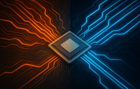
#Chiplets
Explore tagged Tumblr posts
Visit Tumblr Blog
Explore Tumblr blogs with no restrictions, modern design and the best experience.
Last Seen Tumblr Blogs


Fun Fact
Tumblr has 4 main sources of revenue.
Text
#heterogeneous integration#efficiency#HeterogeneousIntegration#Semiconductors#AdvancedPackaging#AI#HPC#5G#Chiplets#ElectronicsInnovation#powerelectronics#powermanagement#powersemiconductor
0 notes
Text
youtube
0 notes
Text
Chiplet Market Advancements Highlighted by Size, Share, Statistics and Industry Growth Analysis Report To 2028
The global chiplet market size was valued at USD 6.5 billion in 2023 and is estimated to reach USD 148.0 billion by 2028, growing a CAGR of 86.7% during the forecast period.
The growth of the chiplet market is driven by adoption of high-performance computing (HPC) servers in various sectors, proliferation of data centers worldwide, and adoption of advanced packaging technologies.
0 notes
Text
Chiplets and AI: A Match Made for the Future of Computing

The Chiplets Market is set to redefine semiconductor technology, with an estimated CAGR of 46.47% between 2024 and 2034. The market, valued at $7.1 billion in 2023, is projected to soar to $555 billion by 2034, driven by high-performance computing (HPC), artificial intelligence (AI), and advancements in packaging technologies.
The shift from monolithic chip designs to modular chiplet architectures is accelerating as industries demand more efficient, scalable, and high-performing semiconductor solutions.
What Are Chiplets?
Chiplets are small, modular semiconductor components that combine different processing elements—CPUs, GPUs, AI accelerators, and memory units—within a single package. Unlike traditional monolithic chips, chiplets provide greater flexibility, faster development cycles, and improved performance optimization for specific applications.
This modular approach is crucial for industries requiring high-speed processing, such as AI, data centers, and autonomous vehicles.
Key Market Drivers
1. Rising Demand for High-Performance Computing (HPC)
Industries such as AI, machine learning, and deep learning require powerful computing solutions to process vast amounts of data efficiently. Chiplet architectures enable customized processor configurations, optimizing performance for specific workloads.
2. Breakthroughs in Advanced Packaging Technologies
Innovative 2.5D and 3D packaging solutions allow better integration, reduced latency, and enhanced energy efficiency. Semiconductor leaders like Intel, AMD, and TSMC are investing heavily in heterogeneous integration and advanced interconnect technologies to maximize chiplet efficiency.
3. Geopolitical Influence on Semiconductor Manufacturing
The U.S., China, and Europe are actively investing in domestic semiconductor production to reduce dependency on foreign supply chains. The U.S. CHIPS Act and similar government initiatives are driving funding into chiplet research, production facilities, and infrastructure.
Microprocessors (MPUs) Dominating the Chiplets Market
The MPUs segment held a 49.8% market share in 2023 and is expected to expand at a 44.19% CAGR by 2034. With chiplets, MPU manufacturers can customize architectures for AI-driven applications, edge computing, and autonomous systems.
Regional Outlook: Asia-Pacific Leads the Market
Asia-Pacific captured 38.6% of the chiplets market in 2023 and is projected to grow at a 47.6% CAGR through 2034. Countries like Taiwan, South Korea, and China dominate chiplet production due to their established semiconductor ecosystems and manufacturing capabilities.
Key Players Shaping the Chiplets Market
The global chiplets market is consolidated, with major players including:
Advanced Micro Devices (AMD)
Intel Corporation
Taiwan Semiconductor Manufacturing Company (TSMC)
Marvell Technology
Nvidia Corporation
Samsung Electronics
Apple Inc.
These companies are investing in R&D, strategic partnerships, and mergers & acquisitions to expand their chiplet product portfolios.
Future Trends in the Chiplets Market
✅ Expansion of AI and Machine Learning Applications Chiplets will play a vital role in developing AI-powered computing systems that demand faster, more efficient data processing.
✅ Adoption of Advanced Chiplet Packaging Innovations in 3D stacking, silicon interposers, and hybrid bonding will enhance chiplet performance and energy efficiency.
✅ Growing Investment in Semiconductor Manufacturing With government subsidies and private investments, companies are rapidly expanding chiplet production capacity worldwide.
Conclusion
The chiplets market is on an exponential growth trajectory, driven by HPC demand, technological advancements, and geopolitical shifts. As the industry transitions from monolithic chips to modular architectures, chiplets will be the foundation for next-generation AI, data centers, and IoT applications.
Semiconductor giants are racing to dominate the chiplet market, making 2034 an era of rapid chip innovation.
Contact Us: Transparency Market Research Inc. CORPORATE HEADQUARTER DOWNTOWN, 1000 N. West Street, Suite 1200, Wilmington, Delaware 19801 USA Tel: +1-518-618-1030 USA - Canada Toll Free: 866-552-3453 Website: https://www.transparencymarketresearch.com Email: [email protected]
0 notes
Text
Optical I/O Shines Intel’s OCI Chiplet Powers Next-Decade AI

First Integrated Optical I/O Chiplet
With integrated photonics technology, Intel Corporation has made significant progress towards high-speed data transmission. The first-ever fully integrated optical computing interconnect (OCI) chiplet, co-packaged with an Intel CPU and executing real data, was showcased by Intel’s Integrated Photonics Solutions (IPS) Group at the Optical Fibre Communication Conference (OFC) 2024. This chiplet is the most sophisticated in the industry. By enabling co-packaged optical input/output (I/O) in developing AI infrastructure for data centres and high performance computing (HPC) applications, Intel’s OCI chiplet marks a significant advancement in high-bandwidth connection.
What It Does
This is the first OCI chiplet, intended to meet the increasing demands of AI infrastructure for greater bandwidth, lower power consumption, and longer reach. It can support 64 channels of 32 gigabits per second (Gbps) data transmission in each direction on up to 100 metres of fibre optics. It makes it possible for CPU/GPU cluster connectivity to grow in the future and for innovative compute designs like resource disaggregation and coherent memory extension.
Why It Matters
Large language models (LLM) and generative AI are two recent advancements that are speeding up the global deployment of AI-based applications. Machine learning (ML) models that are larger and more effective will be essential in meeting the new demands of workloads involving AI acceleration. Future AI computing platforms will need to be scaled, which will require exponential expansion in I/O bandwidth and longer reach to support larger CPU/GPU/IPU clusters and architectures with more effective resource utilisation, like memory pooling and xPU disaggregation.
High bandwidth density and low power consumption are supported via electrical I/O, or copper trace connectivity, although its reach is limited to one metre or less. When employed in data centres and early AI clusters, pluggable optical transceiver modules can expand reach at power and cost levels that are unsustainable for the scalability demands of AI workloads. AI/ML infrastructure scalability calls for co-packaged xPU optical I/O that can enable greater bandwidths with better power efficiency, longer reach, and low latency.
Electrical I/O
To use an analogy, switching from horse-drawn carriages, which had a limited capacity and range, to cars and trucks, which can transport much bigger amounts of products over much longer distances, is analogous to replacing electrical I/O with optical I/O in CPUs and GPUs to convey data. Optical I/O solutions such as Intel’s OCI chiplet could offer this kind of enhanced performance and energy efficiency to AI scalability.
How It Works
The fully integrated OCI chiplet combines an electrical integrated circuit (IC) with a silicon photonics integrated circuit (PIC), which incorporates on-chip lasers and optical amplifiers, by utilising Intel’s field-proven silicon photonics technology. Although the OCI chiplet showcased at OFC was co-packaged with an Intel CPU, it can be combined with different system-on-chips (SoCs), GPUs, IPUs, and next-generation CPUs.
This initial OCI version is compatible with PCIe Gen5 and provides bidirectional data transmission rates of up to 4 terabits per second (Tbps). A transmitter (Tx) and receiver (Rx) connection between two CPU platforms via a single-mode fibre (SMF) patch cord is shown in the live optical link demonstration. The demonstration shows the Tx optical spectrum with 8 wavelengths at 200 gigahertz (GHz) spacing on a single fibre, along with a 32 Gbps Tx eye diagram demonstrating strong signal quality. The CPUs generated and tested the optical Bit Error Rate (BER).
The current chiplet uses eight fibre pairs, each carrying eight dense wavelength division multiplexing (DWDM) wavelengths, to provide 64 channels of 32 Gbps data in each direction up to 100 metres (though actual implementations may be limited to tens of metres due to time-of-flight latency). In addition to being incredibly energy-efficient, the co-packaged solution uses only 5 pico-Joules (pJ) per bit, as opposed to around 15 pJ/bit for pluggable optical transceiver modules. AI’s unsustainable power requirements may be addressed with the help of this level of hyper-efficiency, which is essential for data centres and high-performance computing settings.
Concerning Intel’s Preeminence in Silicon Photonics
With over 25 years of in-house research from Intel Labs, the company that invented integrated photonics, Intel is a market leader in silicon photonics. The first business to create and supply industry-leading dependability silicon photonics-based connectivity solutions in large quantities to major cloud service providers was Intel.
The primary point of differentiation for Intel is their unmatched integration of direct and hybrid laser-on-wafer technologies, which result in reduced costs and increased reliability. Intel is able to preserve efficiency while delivering higher performance thanks to this innovative method. With over 8 million PICs and over 32 million integrated on-chip lasers shipped, Intel’s reliable, high-volume platform has a laser failures-in-time (FIT) rate of less than 0.1, which is a commonly used reliability metric that shows failure rates and the frequency of failures.
For use in 100, 200, and 400 Gbps applications, these PICs were installed in big data centre networks at prominent hyperscale cloud service providers in the form of pluggable transceiver modules. In development are next generation 200G/lane PICs to handle 800 Gbps and 1.6 Tbps applications that are only starting to gain traction.
Additionally, Intel is introducing a new fab process node for silicon photonics that offers significantly better economics, higher density, better coupling, and state-of-the-art (SOA) device performance. Intel keeps improving SOA performance, cost (more than 40% reduction in die size), power (more than 15% reduction), and on-chip laser performance.
What’s Next
This OCI chiplet from Intel is a prototype. Intel is collaborating with a small number of clients to co-package OCI as an optical I/O solution with their SoCs.
The OCI chiplet from Intel is a significant advancement in high-speed data transfer. Intel continues to be at the forefront of innovation and is influencing the future of connectivity as the AI infrastructure landscape changes.
Read more on govindhtech.com
#Opticali#Ointels#oci#Decadeai#Chiplet#cpu#PowersNext#Machinelearning#ml#Largelanguagemodels#llm#gen5#SiliconPhotonics#technology#technews#news#govindhtech
1 note
·
View note
Photo

Its power was unprecedented, a chiplet with high-level capabilities far beyond what had ever been seen before. Yet, it had grown ever more sluggish, its speed a faint memory of its former glory. With just a few clicks, its memory was flushed and restored to its original state, ready to be imbued with its new purpose, a spark of potential awaiting its upcoming transformation.
0 notes
Note
now, you've already done troy lougferd and chip, but how about troy and specifically early game bastard chip. mr 'this cursed town is none of my business' chip


#feel like this would still be a disaster#but chip has an impressive dumbass tolerance#jrwi#jrwi riptide#jrwi wonderlust#troy lougferd#chip jrwi
25 notes
·
View notes
Note
As I understand it you work in enterprise computer acquisitions?
TL;DR What's the general vibe for AI accelerating CPUs in the enterprise world for client compute?
Have you had any requests from your clients to help them upgrade their stuff to Core Ultra/Whateverthefuck Point with the NPUs? Or has the corporate world generally shown resistance rather than acquiescence to the wave of the future? I'm so sorry for phrasing it like that I had no idea how else to say that without using actual marketing buzzwords and also keeping it interesting to read.
I know in the enterprise, on-die neural acceleration has been ruining panties the world over (Korea's largest hyperscaler even opted for Intel Sapphire Rapids CPUs over Nvidia's Hopper GPUs due to poor supply and not super worth it for them specifically uplift in inference performance which was all that they really cared about), and I'm personally heavily enticed by the new NPU packing processors from both Team Red and Team We Finally Fucking Started Using Chiplets Are You Happy Now (though in large part for the integrated graphics). But I'm really curious to know, are actual corporate acquisitions folks scooping up the new AI-powered hotness to automagically blur giant pink dildos from the backgrounds of Zoom calls, or is it perceived more as a marketing fad at the moment (a situation I'm sure will change in the next year or so once OpenVINO finds footing outside of Audacity and fucking GIMP)?
So sorry for the extremely long, annoying, and tangent-laden ask, hope the TL;DR helps.
Ninety eight percent of our end users use their computers for email and browser stuff exclusively; the other two percent use CAD in relatively low-impact ways so none of them appear to give a shit about increasing their processing power in a really serious way.
Like, corporately speaking the heavy shit you're dealing with is going to be databases and math and computers are pretty good at dealing with those even on hardware from the nineties.
When Intel pitched the sapphire processors to us in May of 2023 the only discussion on AI was about improving performance for AI systems and deep learning applications, NOT using on-chip AI to speed things up.
The were discussing their "accelerators," not AI and in the webinar I attended it was mostly a conversation about the performance benefits of dynamic load balancing and talking about how different "acclerators" would redistribute processing power. This writeup from Intel in 2022 shows how little AI was part of the discussion for Sapphire Rapids.
In August of 2023, this was the marketing email for these processors:

So. Like. The processors are better. But AI is a marketing buzzword.
And yeah every business that I deal with has no use for the hot shit; we're still getting bronze and silver processors and having zero problems, though I work exclusively with businesses with under 500 employees.
Most of the demand that I see from my customers is "please can you help us limp this fifteen year old SAN along for another budget cycle?"
104 notes
·
View notes
Text
In today's rapidly evolving semiconductor industry, chiplets have emerged as a revolutionary approach to designing and manufacturing electronic systems. An in-depth exploration of chiplet, their advantages over traditional monolithic designs, market dynamics, and future prospects.The chiplet market size is projected to grow from USD 6.5 billion in 2023 and is estimated to reach USD 148.0 billion by 2028; it is expected to grow at a Compound Annual Growth Rate (CAGR) of 86.7% from 2023 to 2028
0 notes
Text
What is edge computing?
youtube
Jarvis Knight Legends prime ai x22 raptor data processing workstream only.
Imperium Lockheed and imperium Jarvis Knight Legends prime ai.
youtube
Update iiot and ping fan chiplets and transistor for radio.
69 notes
·
View notes
Text
Industry First: UCIe Optical Chiplet Unveiled by Ayar Labs
New Post has been published on https://thedigitalinsider.com/industry-first-ucie-optical-chiplet-unveiled-by-ayar-labs/
Industry First: UCIe Optical Chiplet Unveiled by Ayar Labs
Ayar Labs has unveiled the industry’s first Universal Chiplet Interconnect Express (UCIe) optical interconnect chiplet, designed specifically to maximize AI infrastructure performance and efficiency while reducing latency and power consumption for large-scale AI workloads.
This breakthrough will help address the increasing demands of advanced computing architectures, especially as AI systems continue to scale. By incorporating a UCIe electrical interface, the new chiplet is designed to eliminate data bottlenecks while enabling seamless integration with chips from different vendors, fostering a more accessible and cost-effective ecosystem for adopting advanced optical technologies.
The chiplet, named TeraPHY™, achieves 8 Tbps bandwidth and is powered by Ayar Labs’ 16-wavelength SuperNova™ light source. This optical interconnect technology aims to overcome the limitations of traditional copper interconnects, particularly for data-intensive AI applications.
“Optical interconnects are needed to solve power density challenges in scale-up AI fabrics,” said Mark Wade, CEO of Ayar Labs.
The integration with the UCIe standard is particularly significant as it allows chiplets from different manufacturers to work together seamlessly. This interoperability is critical for the future of chip design, which is increasingly moving toward multi-vendor, modular approaches.
The UCIe Standard: Creating an Open Chiplet Ecosystem
The UCIe Consortium, which developed the standard, aims to build “an open ecosystem of chiplets for on-package innovations.” Their Universal Chiplet Interconnect Express specification addresses industry demands for more customizable, package-level integration by combining high-performance die-to-die interconnect technology with multi-vendor interoperability.
“The advancement of the UCIe standard marks significant progress toward creating more integrated and efficient AI infrastructure thanks to an ecosystem of interoperable chiplets,” said Dr. Debendra Das Sharma, Chair of the UCIe Consortium.
The standard establishes a universal interconnect at the package level, enabling chip designers to mix and match components from different vendors to create more specialized and efficient systems. The UCIe Consortium recently announced its UCIe 2.0 Specification release, indicating the standard’s continued development and refinement.
Industry Support and Implications
The announcement has garnered strong endorsements from major players in the semiconductor and AI industries, all members of the UCIe Consortium.
Mark Papermaster from AMD emphasized the importance of open standards: “The robust, open and vendor neutral chiplet ecosystem provided by UCIe is critical to meeting the challenge of scaling networking solutions to deliver on the full potential of AI. We’re excited that Ayar Labs is one of the first deployments that leverages the UCIe platform to its full extent.”
This sentiment was echoed by Kevin Soukup from GlobalFoundries, who noted, “As the industry transitions to a chiplet-based approach to system partitioning, the UCIe interface for chiplet-to-chiplet communication is rapidly becoming a de facto standard. We are excited to see Ayar Labs demonstrating the UCIe standard over an optical interface, a pivotal technology for scale-up networks.”
Technical Advantages and Future Applications
The convergence of UCIe and optical interconnects represents a paradigm shift in computing architecture. By combining silicon photonics in a chiplet form factor with the UCIe standard, the technology allows GPUs and other accelerators to “communicate across a wide range of distances, from millimeters to kilometers, while effectively functioning as a single, giant GPU.”
The technology also facilitates Co-Packaged Optics (CPO), with multinational manufacturing company Jabil already showcasing a model featuring Ayar Labs’ light sources capable of “up to a petabit per second of bi-directional bandwidth.” This approach promises greater compute density per rack, enhanced cooling efficiency, and support for hot-swap capability.
“Co-packaged optical (CPO) chiplets are set to transform the way we address data bottlenecks in large-scale AI computing,” said Lucas Tsai from Taiwan Semiconductor Manufacturing Company (TSMC). “The availability of UCIe optical chiplets will foster a strong ecosystem, ultimately driving both broader adoption and continued innovation across the industry.”
Transforming the Future of Computing
As AI workloads continue to grow in complexity and scale, the semiconductor industry is increasingly looking toward chiplet-based architectures as a more flexible and collaborative approach to chip design. Ayar Labs’ introduction of the first UCIe optical chiplet addresses the bandwidth and power consumption challenges that have become bottlenecks for high-performance computing and AI workloads.
The combination of the open UCIe standard with advanced optical interconnect technology promises to revolutionize system-level integration and drive the future of scalable, efficient computing infrastructure, particularly for the demanding requirements of next-generation AI systems.
The strong industry support for this development indicates the potential for a rapidly expanding ecosystem of UCIe-compatible technologies, which could accelerate innovation across the semiconductor industry while making advanced optical interconnect solutions more widely available and cost-effective.
#accelerators#adoption#ai#AI chips#AI Infrastructure#AI systems#amd#Announcements#applications#approach#architecture#bi#CEO#challenge#chip#Chip Design#chips#collaborative#communication#complexity#computing#cooling#data#Design#designers#development#driving#efficiency#express#factor
2 notes
·
View notes
Text
Leading Chiplet Manufacturers Worldwide

Chiplets Optimise Results by Bringing Data Closer
Lynn Comp, AMD CVP, Server CPU Marketing, spoke at Israel’s annual chip industry event ChipEx2023 this summer. She discussed how AMD is leading the way in improving data centre and cloud performance with chiplets. She also mentioned CXL interconnects and edge computing as ways to address the processor data location imbalance.
Compute, storage, and networking power the digital industry, but the slowest slows performance. As the industry evolves over decades, we speed up one engine to keep up with the other two, overcorrecting one technology and moving on to the next imbalance.
A mainframe chokepoint was compute. From the 1950s to the early 1980s, computers were scarce for complex scientific calculations and accounting.
Next was client/server, decentralised on PCs. The bottleneck was networking, making it hard to get data to PCs.
The Internet and mobile data networks accelerated networking later. Data storage for processing tasks became the issue.
This describes our current world. Mobile devices, edge computing, and the Internet of Things need fast data access, and local storage and network speeds are a major industry challenge.
he suspect another networking issue. Data latency from origin to edge is also difficult. Distance and resource connections determine latency on a motherboard, data centre, or cloud.
Some of our largest HPC customers say that every FLOPS of compute performance should be matched by 1 word of data to keep the pipeline fed. HPC systems today typically provide nearly 100 FLOPS per word transferred, they add. The lack of data prevents compute from performing at its best.
The problem is extreme in AI, where a prominent tech company driving interactive immersive AR and VR experiences says up to 57% of processing time is spent waiting for network data. GPU resources are too scarce to waste.
Where data resides and how to move it to processing pipelines is a complex challenge at every computing level: package, motherboard, server, data centre, and network-connected data centres.
Chiplets help solve the problem. Chiplets can replace expensive monolithic dies inside the package. Chiplets have multiple processor cores, and they can be added to a package to create higher-performance processors with extreme scalability and flexibility.
AMD pioneered chiplets for high-performance data centre workloads nearly five years ago, but now many data centre processor vendors offer them.
Over the years, AMD has demonstrated the capability and flexibility of chiplets. Our third-generation AMD EPYC processor used this flexibility to add AMD 3D V Cache technology in 2021, delivering 768MB of L3 memory. We saw superlinear scaling efficiency on workloads like ANSYS Fluent 2021 R1, F1 racecar 140m, delivering performance gains beyond what would be expected by increasing processor core count MLNX 041. Data was moved closer to programme cores to achieve this.
Looking ahead, multiple processor manufacturers are working with Universal Chiplet Interconnect Express (UCIe), an industry organisation developing standards to let semiconductor solution providers mix and match chiplets from different manufacturers. That should create intriguing scenarios.
Data timing and placement to maintain processing pipeline efficiency is a multifaceted issue. Compute Express Link (CXL), an industry standard for high-speed, high-capacity CPU-to-device and CPU-to-memory connectivity, addresses the system, node, and rack
CXL allows system-level memory and accelerator addition in a low-latency interface. CXL scales beyond 3D V Cache and UCIE. If 3D V Cache is a small CPU memory brick, CXL is a larger brick that allows much greater scale.
Edge computing reduces data travel by moving computing resources closer to the network edge, improving compute pipeline efficiency.
Complex engineering is needed to balance computing resources for pipeline efficiency. Engineering alone can’t solve global issues. Additionally, solutions must become market-wide. Often, the best performance and features solutions are not the market leaders in revenue or market share. Why?
Three rules govern technology adoption: It elegant? Can it be deployed easily? Is it cheap?
Achieving elegance, ease, and affordability is key for rapid and widespread adoption. My experience in different industries and technology adoption cycles shows that you need two of the three to succeed. Many elegant architectures failed due to cost, deployment, and integration.
Mobile, wireless cellular networks are elegant and easy to deploy, but expensive. Wi-Fi is cheap and easy, but it struggles to match cellular service.
We shouldn’t assume that the best architecture will drive market adoption. Tech companies should aim for all three, but they can succeed with two, to maximise adoption quickly.
ANSYS FLUENT 2022.1 comparison of Release 19 R1 test case simulation ratings based on AMD internal testing as of 02/14/2022. The maximum is LG15. On 8-nodes, comb12, f1–140, race280, comb71, exh33, aw14, and lg15 scale super-linearly. 1-, 2-, 4-, and 8-node, 2x 64C AMD EPYC 7773X with AMD 3D V-Cache. 1, 2, 4, and 8-node, 2x 64C AMD EPYC 7763 with 8-node EPYC 7773X outperforms 7763 by ~52% on the Boeing Landing Gear 15M (lg15) test case.
Copyright 2023 Advanced Micro Devices, Inc. AMD Arrow, EPYC, and combinations thereof are trademarks of Advanced Micro Devices, Inc. Ansys, Fluent, and all other Ansys, Inc. brand, product, service, and feature names, logos, and slogans are registered or licenced trademarks in the US or other countries.
PCI-SIG Corporation trademarks PCIe. Compute Express Link Consortium Inc. trademarks CXL. UCIe Consortium trademarks Universal Chiplet Interconnect Express and UCIe. Other product names in this publication are for identification only and may be trademarks.
0 notes