#Circuit board failure analysis
Explore tagged Tumblr posts
Visit Tumblr Blog
Explore Tumblr blogs with no restrictions, modern design and the best experience.
Last Seen Tumblr Blogs


Fun Fact
130K people were victims of a chain letter scam that affected Tumblr in May 2011.
Text
Circuit board fault analysis: revealing the components most prone to problems
I published an article "Guidelines for Identification and Troubleshooting of Capacitor, Resistor, and Operational Amplifier Faults", article link: https://www.dhsic.com/news/97
#Circuit board failure analysis#Component Failure Guide#Components#circuit board#capacitance#resistance#Operational Amplifier
0 notes
Text
Electronics Manufacturing: Trends and Industry Insights


In an industry defined by continuous development and exacting standards, electronics manufacturing is a critical driver of modern technology. From everyday consumer goods to complex industrial systems, the journey of each component begins with thoughtful engineering, rigorous production practices, and strong supplier relationships. Based in Arundel, West Sussex, Arrival Electronics Limited stands at the heart of this field, working closely with clients to meet the evolving needs of today’s electronic markets.
This article explores the inner workings of the electronic components industry—what drives it, the trends shaping it, and what decision-makers should understand when choosing the right components or partners. Whether you're a design engineer, purchasing manager, or systems integrator, a clear understanding of this sector will help support better outcomes for your business and your customers.
Understanding the Electronics Manufacturing Process
The process involves assembling electronic components into complete, functional products ready for use or distribution. This can include simple printed circuit board assemblies or more intricate systems involving hundreds of interconnected parts. The process demands consistent quality, traceability, and efficient logistics from start to finish.
The primary stages include:
Component Sourcing: Reliable supply chains and vetted manufacturers are essential. Components must meet specifications, often under strict time constraints and regulatory compliance requirements.
PCB Assembly: Surface mount technology (SMT) and through-hole assembly are key methods used in creating circuit boards. Attention to detail is vital here, as even minor errors can result in failure during testing or deployment.
Testing and Inspection: Functional tests, visual inspections, and X-ray analysis are just some of the methods used to confirm product reliability. These steps help ensure products perform as intended once installed.
Final Assembly and Packaging: After testing, products are assembled into enclosures, labeled, and prepared for shipment, often requiring anti-static handling, thermal protection, or precise labeling practices.
Producing electronic products requires more than tools and machines—it’s about consistency, communication, and adapting to specific project demands.
Key Trends Shaping Today’s Production Landscape
As technology progresses, the electronics sector must constantly adjust. Here are several trends affecting the direction of the industry:
1. Miniaturization
Devices are shrinking, but performance expectations remain high. Engineers must work with tighter tolerances and more complex component configurations. This puts pressure on design and manufacturing teams to align on specifications early in the project lifecycle.
2. Demand for Custom Solutions
Many industries—such as medical, aerospace, and renewable energy—are looking for specialized circuit designs rather than one-size-fits-all solutions. Manufacturers that can provide flexible production runs, in-depth technical consultation, and fast turnarounds are in demand.
3. Supply Chain Resilience
The global component shortage has made it clear how critical supply chain visibility and reliability are. Businesses are increasingly working with sourcing partners that can offer a wide selection of inventory, cross-reference alternatives, and reduce exposure to delays.
4. Sustainability in Manufacturing
There is growing interest in sustainable production practices, including RoHS compliance, lead-free soldering, and energy-efficient factory environments. Electronics manufacturers must respond by implementing responsible processes and working with suppliers who share the same values.
Why Quality and Compliance Matter More Than Ever
When it comes to production and assembly, quality is more than a buzzword—it's a measurable requirement. A faulty capacitor or misaligned connector can result in expensive system failures, regulatory issues, or even safety concerns.
To meet modern expectations, manufacturers must:
Follow ISO-certified procedures
Maintain full traceability of components
Ensure regulatory compliance across target markets (CE, UL, REACH, etc.)
Maintain strong documentation for every stage of the process
Choosing a manufacturing partner with a deep understanding of international standards and a history of consistent delivery helps reduce risks and keeps projects on track.


What Sets Our Manufacturing Services Apart
Our approach is built around delivering practical, cost-effective manufacturing solutions tailored to meet each customer’s unique requirements. By applying lean manufacturing principles, we help clients reduce waste, improve efficiency, and gain measurable value in every step of the process.
Key benefits include:
Lower inventory demands
Reduced total acquisition costs
Supply chain resilience through multiple inventory locations
Improved product quality
Consistent, on-time delivery you can rely on
What to Consider When Choosing a Technical Assembly Partner
Finding a reliable service provider is about more than pricing or proximity. Here are key factors to evaluate:
1. Technical Expertise
Look for teams that can interpret your bill of materials (BOM), understand the application of each component, and make suggestions where appropriate. This ensures that your products are not only assembled correctly but also designed for success.
2. Supplier Relationships
Does the provider have access to a wide range of reputable manufacturers? Can they offer alternatives when primary parts are unavailable? These questions are especially important during global shortages or when dealing with niche specifications.
3. Project Flexibility
Can they accommodate small production runs or prototype builds? Can they ramp up to meet large-scale demand? Flexibility ensures that your partner can adjust alongside your project’s lifecycle.
4. Transparent Communication
Regular updates, clear technical feedback, and documentation of every phase help create confidence. Projects that lack open communication are more likely to experience delays and misunderstandings.
5. End-to-End Support
From early-stage design reviews to post-sale technical queries, the most reliable firms remain actively involved throughout the entire process. They provide ongoing value and ensure long-term reliability, not just short-term assembly.
Meeting Industry Demands: A Practical Approach
The sector serves a wide range of industries, including automotive, medical, aerospace, defense, consumer goods, and industrial automation.. Each sector has its own regulatory environment, tolerances, and expectations for delivery timeframes.
For instance:
Medical devices often require cleanroom assembly and documentation to meet stringent approval standards.
Automotive components must withstand harsh environmental conditions and vibration without performance degradation.
Aerospace systems demand redundancy, traceability, and exact part performance for mission-critical applications.
As these requirements grow more complex, manufacturing partners must respond with tailored approaches—balancing engineering support, materials expertise, and practical experience.
Building Long-Term Success with Trusted Partners
Supply chain challenges, new materials, evolving regulations—these realities require ongoing adaptation. Companies that treat production as a strategic function rather than a transactional service gain a competitive edge.
To succeed, it's essential to work with a partner that:
Understands your industry
Invests in continuous improvement
Keeps up with changing compliance rules
Prioritizes reliability over shortcuts
This is where experience matters. Businesses with a consistent record of on-time delivery, error-free builds, and in-depth component knowledge provide a firm foundation for long-term growth.
About Arrival Electronics Limited
Located in West Sussex, Arrival Electronics Limited is an independent electronic component supplier with deep roots in the electronics manufacturing sector. Known for its technical approach, reliable stock availability, and excellent customer support, the company serves clients across a wide range of industries—including automotive, broadcast, industrial, and aerospace.
Their team offers more than just product sourcing—they offer insight. They collaborate with manufacturers and design engineers to ensure all supplied parts meet application-specific needs. Whether supporting high-mix production or long-term component supply, Arrival Electronics Limited provides dependable service and extensive market knowledge that adds lasting value.
Final Thoughts
Electronics manufacturing is not just a mechanical process; it's a critical function that supports the quality, safety, and performance of the technology we depend on every day. Businesses that understand its nuances are better positioned to deliver products that work as intended, meet compliance goals, and perform reliably over time.
For companies seeking support in this complex space, Arrival Electronics Limited stands as a resourceful and experienced partner. With technical insight, customer dedication, and a clear understanding of today’s component landscape, they help businesses navigate the challenges and practical realities of bringing modern electronic products to market.
0 notes
Text
Precision Solutions for Defence and Aerospace Electronics

In the high-stakes sectors of defence and aerospace, reliability, performance, and precision are non-negotiable. Whether it's mission-critical communications equipment, avionics systems, or advanced sensor technologies, the quality of electronic manufacturing plays a pivotal role in national security, flight safety, and technological superiority. This is where defence and aerospace electronic manufacturing becomes an essential pillar of innovation and resilience—and where trusted providers like Masters & Young excel.
With decades of proven expertise, Masters & Young specialises in delivering cutting-edge technology and precision-engineered solutions tailored to meet the exacting standards of the defence and aerospace industries. Our commitment to innovation, quality, and compliance ensures that every component we manufacture performs flawlessly, even under the most extreme conditions.
Why Defence and Aerospace Require Specialised Electronic Manufacturing
The demands of defence and aerospace electronic manufacturing far exceed those of consumer or general industrial electronics. The equipment must operate in highly controlled and often hostile environments—extreme temperatures, high G-forces, electromagnetic interference, and more. Components must not only perform consistently but also adhere to strict regulatory frameworks and certifications such as ISO 9001, AS9100, and IPC standards.
Critical applications in these sectors include:
Military communication systems
Guidance and navigation electronics
Radar and surveillance systems
Flight control modules
Electronic warfare and cybersecurity infrastructure
Satellite and space-based electronics
Given the complexity and importance of these applications, manufacturers must employ robust quality control, advanced testing methodologies, and skilled engineering expertise to deliver compliant, high-performance products.
Masters & Young: Leading the Way in Defence and Aerospace Solutions
At Masters & Young, our reputation is built on decades of consistent delivery, technical innovation, and deep understanding of the unique requirements of defence and aerospace projects. We provide end-to-end electronic manufacturing services (EMS), from design consultation and prototyping to production, testing, and compliance certification.
Our core strengths include:
Precision Engineering: Every circuit board and electronic assembly is crafted with attention to detail and adherence to tight tolerances, ensuring optimal function and longevity.
Advanced Manufacturing Capabilities: Our facilities are equipped with the latest surface mount technology (SMT), automated optical inspection (AOI), and X-ray inspection tools to ensure the highest manufacturing quality.
Custom Solutions: We understand that each defence or aerospace application is unique. That’s why we offer tailored solutions that align with specific client objectives, environmental demands, and operational protocols.
Compliance & Certification: Masters & Young operates within stringent defence and aerospace manufacturing frameworks, offering full traceability, secure documentation, and compliance with relevant industry standards.
The Importance of Reliability in Defence and Aerospace Electronics
When it comes to defence and aerospace electronic manufacturing, there is no room for error. System failures can lead to mission compromise, loss of critical assets, or even loss of life. That’s why our engineering and production teams follow a rigorous quality management system that includes:
In-depth testing and validation protocols
Environmental stress screening (ESS)
Functional and in-circuit testing (ICT)
EMI/EMC testing for compliance
Failure mode and effects analysis (FMEA)
These practices ensure that each product not only meets but exceeds performance benchmarks and reliability expectations.
Collaborating with Defence and Aerospace Industry Leaders
Masters & Young has long-standing partnerships with government agencies, defence contractors, and aerospace innovators. Our proven track record of supporting classified and non-classified projects has positioned us as a preferred supplier for high-performance, mission-critical electronics across Australia and beyond.
Whether it’s upgrading radar systems, developing electronic control units (ECUs), or manufacturing embedded systems for aircraft and defence vehicles, we deliver solutions that push boundaries while maintaining the utmost quality and security.
Final Thoughts
The future of national defence and aerospace innovation hinges on the strength of its technology—and that begins with superior electronic manufacturing. At Masters & Young, we take pride in being at the forefront of this crucial sector, offering reliable, precise, and compliant defence and aerospace electronic manufacturing solutions.
If you’re seeking a partner who understands the stakes and delivers with unmatched expertise, trust Masters & Young to meet your requirements with precision, integrity, and innovation.
0 notes
Text
Precision Solutions for Defence and Aerospace Electronics

In the high-stakes sectors of defence and aerospace, reliability, performance, and precision are non-negotiable. Whether it's mission-critical communications equipment, avionics systems, or advanced sensor technologies, the quality of electronic manufacturing plays a pivotal role in national security, flight safety, and technological superiority. This is where defence and aerospace electronic manufacturing becomes an essential pillar of innovation and resilience—and where trusted providers like Masters & Young excel.
With decades of proven expertise, Masters & Young specialises in delivering cutting-edge technology and precision-engineered solutions tailored to meet the exacting standards of the defence and aerospace industries. Our commitment to innovation, quality, and compliance ensures that every component we manufacture performs flawlessly, even under the most extreme conditions.
Why Defence and Aerospace Require Specialised Electronic Manufacturing
The demands of defence and aerospace electronic manufacturing far exceed those of consumer or general industrial electronics. The equipment must operate in highly controlled and often hostile environments—extreme temperatures, high G-forces, electromagnetic interference, and more. Components must not only perform consistently but also adhere to strict regulatory frameworks and certifications such as ISO 9001, AS9100, and IPC standards.
Critical applications in these sectors include:
Military communication systems
Guidance and navigation electronics
Radar and surveillance systems
Flight control modules
Electronic warfare and cybersecurity infrastructure
Satellite and space-based electronics
Given the complexity and importance of these applications, manufacturers must employ robust quality control, advanced testing methodologies, and skilled engineering expertise to deliver compliant, high-performance products.
Masters & Young: Leading the Way in Defence and Aerospace Solutions
At Masters & Young, our reputation is built on decades of consistent delivery, technical innovation, and deep understanding of the unique requirements of defence and aerospace projects. We provide end-to-end electronic manufacturing services (EMS), from design consultation and prototyping to production, testing, and compliance certification.
Our core strengths include:
Precision Engineering: Every circuit board and electronic assembly is crafted with attention to detail and adherence to tight tolerances, ensuring optimal function and longevity.
Advanced Manufacturing Capabilities: Our facilities are equipped with the latest surface mount technology (SMT), automated optical inspection (AOI), and X-ray inspection tools to ensure the highest manufacturing quality.
Custom Solutions: We understand that each defence or aerospace application is unique. That’s why we offer tailored solutions that align with specific client objectives, environmental demands, and operational protocols.
Compliance & Certification: Masters & Young operates within stringent defence and aerospace manufacturing frameworks, offering full traceability, secure documentation, and compliance with relevant industry standards.
The Importance of Reliability in Defence and Aerospace Electronics
When it comes to defence and aerospace electronic manufacturing, there is no room for error. System failures can lead to mission compromise, loss of critical assets, or even loss of life. That’s why our engineering and production teams follow a rigorous quality management system that includes:
In-depth testing and validation protocols
Environmental stress screening (ESS)
Functional and in-circuit testing (ICT)
EMI/EMC testing for compliance
Failure mode and effects analysis (FMEA)
These practices ensure that each product not only meets but exceeds performance benchmarks and reliability expectations.
Collaborating with Defence and Aerospace Industry Leaders
Masters & Young has long-standing partnerships with government agencies, defence contractors, and aerospace innovators. Our proven track record of supporting classified and non-classified projects has positioned us as a preferred supplier for high-performance, mission-critical electronics across Australia and beyond.
Whether it’s upgrading radar systems, developing electronic control units (ECUs), or manufacturing embedded systems for aircraft and defence vehicles, we deliver solutions that push boundaries while maintaining the utmost quality and security.
Final Thoughts
The future of national defence and aerospace innovation hinges on the strength of its technology—and that begins with superior electronic manufacturing. At Masters & Young, we take pride in being at the forefront of this crucial sector, offering reliable, precise, and compliant defence and aerospace electronic manufacturing solutions. If you’re seeking a partner who understands the stakes and delivers with unmatched expertise, trust Masters & Young to meet your requirements with precision, integrity, and innovation.
0 notes
Text
Precision Solutions for Defence and Aerospace Electronics

In the high-stakes sectors of defence and aerospace, reliability, performance, and precision are non-negotiable. Whether it's mission-critical communications equipment, avionics systems, or advanced sensor technologies, the quality of electronic manufacturing plays a pivotal role in national security, flight safety, and technological superiority. This is where defence and aerospace electronic manufacturing becomes an essential pillar of innovation and resilience—and where trusted providers like Masters & Young excel.
With decades of proven expertise, Masters & Young specialises in delivering cutting-edge technology and precision-engineered solutions tailored to meet the exacting standards of the defence and aerospace industries. Our commitment to innovation, quality, and compliance ensures that every component we manufacture performs flawlessly, even under the most extreme conditions.
Why Defence and Aerospace Require Specialised Electronic Manufacturing
The demands of defence and aerospace electronic manufacturing far exceed those of consumer or general industrial electronics. The equipment must operate in highly controlled and often hostile environments—extreme temperatures, high G-forces, electromagnetic interference, and more. Components must not only perform consistently but also adhere to strict regulatory frameworks and certifications such as ISO 9001, AS9100, and IPC standards.
Critical applications in these sectors include:
Military communication systems
Guidance and navigation electronics
Radar and surveillance systems
Flight control modules
Electronic warfare and cybersecurity infrastructure
Satellite and space-based electronics
Given the complexity and importance of these applications, manufacturers must employ robust quality control, advanced testing methodologies, and skilled engineering expertise to deliver compliant, high-performance products.
Masters & Young: Leading the Way in Defence and Aerospace Solutions
At Masters & Young, our reputation is built on decades of consistent delivery, technical innovation, and deep understanding of the unique requirements of defence and aerospace projects. We provide end-to-end electronic manufacturing services (EMS), from design consultation and prototyping to production, testing, and compliance certification.
Our core strengths include:
Precision Engineering: Every circuit board and electronic assembly is crafted with attention to detail and adherence to tight tolerances, ensuring optimal function and longevity.
Advanced Manufacturing Capabilities: Our facilities are equipped with the latest surface mount technology (SMT), automated optical inspection (AOI), and X-ray inspection tools to ensure the highest manufacturing quality.
Custom Solutions: We understand that each defence or aerospace application is unique. That’s why we offer tailored solutions that align with specific client objectives, environmental demands, and operational protocols.
Compliance & Certification: Masters & Young operates within stringent defence and aerospace manufacturing frameworks, offering full traceability, secure documentation, and compliance with relevant industry standards.
The Importance of Reliability in Defence and Aerospace Electronics
When it comes to defence and aerospace electronic manufacturing, there is no room for error. System failures can lead to mission compromise, loss of critical assets, or even loss of life. That’s why our engineering and production teams follow a rigorous quality management system that includes:
In-depth testing and validation protocols
Environmental stress screening (ESS)
Functional and in-circuit testing (ICT)
EMI/EMC testing for compliance
Failure mode and effects analysis (FMEA)
These practices ensure that each product not only meets but exceeds performance benchmarks and reliability expectations.
Collaborating with Defence and Aerospace Industry Leaders
Masters & Young has long-standing partnerships with government agencies, defence contractors, and aerospace innovators. Our proven track record of supporting classified and non-classified projects has positioned us as a preferred supplier for high-performance, mission-critical electronics across Australia and beyond.
Whether it’s upgrading radar systems, developing electronic control units (ECUs), or manufacturing embedded systems for aircraft and defence vehicles, we deliver solutions that push boundaries while maintaining the utmost quality and security.
Final Thoughts
The future of national defence and aerospace innovation hinges on the strength of its technology—and that begins with superior electronic manufacturing. At Masters & Young, we take pride in being at the forefront of this crucial sector, offering reliable, precise, and compliant defence and aerospace electronic manufacturing solutions.
If you’re seeking a partner who understands the stakes and delivers with unmatched expertise, trust Masters & Young to meet your requirements with precision, integrity, and innovation.
0 notes
Text
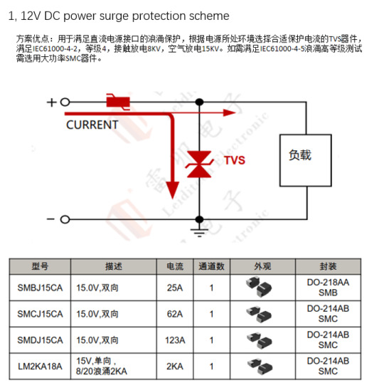
Interface protection design for edge computing gateways
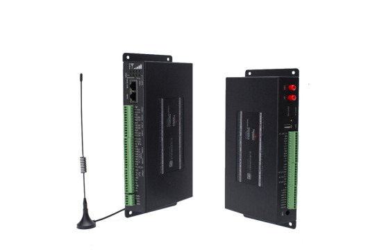
With the rise of the Internet of Things and the popularity of cloud services, a new computing paradigm — edge computing — is beginning to appear in our field of vision. Edge computing advocates processing data at the edge of the network, thereby reducing system response time, protecting data privacy and security, extending battery life, and saving network bandwidth. Current applications are divided into industrial and automotive applications.
Industrial gateways
Industrial gateway is an indispensable device of the industrial Internet of Things, it is like the nerves of the human body, the perceived various types of information to the brain for processing, the brain through the operation to determine what kind of response to do, and then transmitted by the nerves to the limbs of the whole body. The gateway can collect PLC data, do remote maintenance and download programs, and has the functions of edge computing and protocol parsing. Industrial communication gateways can perform message conversion between various network protocols, and their functions can be implemented by a chip, an embedded device or board, or a stand-alone device.
Industrial Edge Computing Gateway Features:
1. Rich interface, support Ethernet, serial port, CAN port, IO port and other equipment access and Ethernet, 2G/3G/4G full Netcom network access;
2. Embedded hundreds of industrial protocols, supporting more than 99% PLC and the vast majority of industrial equipment access;
3. 8GB local storage + SD card support, support local data cache and offline application;
4. Three-in-one serial port, support RS485/RS232/RS422 three kinds of electrical interfaces;
5. Support edge computing, realize data optimization, real-time response, agile connection, model analysis and other services in the edge node of the Internet of Things, and effectively share cloud computing resources to support simultaneous access of multiple devices;
6. Support DC9~36V wide voltage input, adapt to a variety of complex industrial sites;
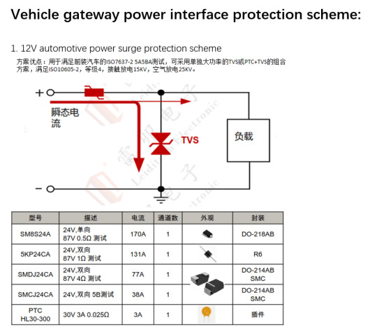
Each interface protection design of the industrial gateway
D-C power supply
Features of the on-board gateway
Due to the particularity of the on-board power supply, all the product power ports taken from the car need to pass the surge load-dump test, Leiditech Electronics provides a professional protection solution for the load-dump test, compared with the industrial gateway, the on-board power supply protection needs are greater.
summary
The interface protection of electronic products needs to use overvoltage protection devices, many engineers realize that they want to use protection devices, but due to improper selection or failure to follow the ESD circuit PCB design principles, resulting in product electrostatic testing or EMC testing does not pass, product verification tests many times, waste of manpower and financial resources, causing product delays to market Things always occur, or over-design, resulting in cost pressure.
Leiditech Electronics specializes in providing customers with EMC design services for electromagnetic compatibility, providing laboratories to do thorough tests, from customers efficient, easy to complete the design, hoping that more customers can quickly pass EMC’s projects and improve product reliability. Leiditech Electronic Electromagnetic Compatibility Laboratory, which provides peripheral electrostatic surge protection reference circuits.
If you’d like to learn more or have any questions, don’t hesitate to reach out:
Visit us at [en.leiditech.com]
EdgeComputing #IndustrialIoT #EMCDesign #ESDProtection #AutomotiveGateway #SmartFactory #IoTDesign #HardwareEngineering #EmbeddedSystems #SurgeProtection #InterfaceDesign #TechBlog #EngineeringLife #ProductDevelopment #DesignTips
0 notes
Text

Abstract Vibration testing is a crucial element in validating the reliability, structural integrity, and durability of components and finished products throughout their operational lifespan. This paper discusses how vibration testing equipment, specifically the LISUN LVD-100KG Electrodynamic Vibration Generator System, plays a pivotal role in determining product resistance to real-world mechanical stresses. By simulating various vibration profiles across multiple axes, this system helps manufacturers meet international standards and improve product designs. Comprehensive performance data, testing configurations, and industry applications are explored alongside comparative analysis, highlighting the significance of modern vibration testing equipment in contemporary quality assurance processes. 1. Introduction In an increasingly demanding consumer and industrial market, ensuring the longevity and robustness of electronic and mechanical products is more critical than ever. Vibration testing equipment serves as a simulation platform that helps evaluate how products behave under operational vibrations. Whether the product is destined for automotive, aerospace, electronics, or household use, it is expected to perform reliably despite constant exposure to mechanical stress. The LISUN LVD-100KG Electrodynamic Vibration Generator System is designed for high-performance vibration simulation, enabling precise testing of product response to mechanical stresses. This paper investigates the utility of such systems, discusses standard testing procedures, and provides analytical results from typical testing scenarios. 2. Importance of Vibration Testing Equipment in Product Development Vibration testing is a foundational step in product development and certification, helping in: • Detecting structural weaknesses • Identifying premature failure risks • Improving packaging designs • Optimizing component layout and materials Without proper vibration simulation, products may suffer from early failures due to resonance, fatigue cracks, or misalignments. Vibration testing equipment facilitates both developmental diagnostics and final validation. Electrodynamic Vibration Generator System LVD-100KG 3. Overview of LISUN LVD-100KG Electrodynamic Vibration Generator System The LISUN LVD-100KG system provides programmable vibration profiles that comply with international standards like IEC, MIL-STD, ISO, and ASTM. The system supports vertical and horizontal test modes, making it suitable for a wide range of product testing applications. Key Features: Parameter Specification Max Load Capacity 100 kg Frequency Range 2–5000 Hz Max Acceleration 100 g Max Displacement 25 mm (peak to peak) Vibration Mode Sine, Random, Shock Axis Support X, Y, Z Cooling System Air-cooled Controller Interface PC-based with programmable sweep profiles The system’s ability to simulate shock and continuous vibration makes it ideal for evaluating resonance, looseness, and material fatigue in components like circuit boards, battery packs, vehicle modules, and consumer electronics. 4. Test Methodologies Supported by Vibration Testing Equipment The LVD-100KG supports several standardized testing methods: 4.1. Sinusoidal Sweep Test Used to find the natural frequency and potential resonances. 4.2. Random Vibration Test Mimics real-world vibration environments such as transportation or operational engine noise. 4.3. Shock Test Applies abrupt pulses to assess resistance to sudden impacts or drops. 4.4. Dwell Test Applies vibration at a fixed frequency for extended durations to study fatigue. 4.5. Transportation Simulation Reproduces shipping and handling conditions to validate packaging and product robustness. 5. Application Scenarios Vibration testing equipment is used across various sectors: Industry Test Objective Example Components Automotive Validate mechanical stability ECU, Sensors, Dashboard Aerospace Ensure performance in flight Avionics, Wiring, Brackets Electronics PCB durability & connector stability Mobile Devices, Laptops Household Appliances Noise and vibration reduction Washing Machines, Compressors Lighting Assess joint and housing endurance LED Drivers, Bulbs 6. Case Study: LED Driver Vibration Test Objective: To assess mechanical robustness and solder joint integrity of LED drivers under operational vibration conditions. Equipment Used: • LISUN LVD-100KG Vibration Testing Equipment • Acceleration sensors • Data acquisition system Test Parameters: Test Mode Sine Sweep Frequency Range 10–1000 Hz Acceleration 10 g Duration 2 hours per axis Axes Tested X, Y, Z Results Summary: Axis Observations X Minor casing vibration, no structural failures Y Slight connector loosening noted Z No anomalies detected The test highlighted potential design improvements in connector attachment methods to enhance product longevity. 7. Software Capabilities and Control Flexibility The LVD-100KG system includes intuitive, PC-based software that offers: • Automatic frequency sweep • Custom test profiles • Real-time data logging • Alarm and shutdown features for test safety • Report generation in CSV and PDF formats Such automation ensures repeatability and minimizes human error, increasing overall test reliability. 8. Compliance and Standards The LVD-100KG meets various global testing standards: Standard Application IEC 60068-2-6 Environmental testing MIL-STD-810G Military-grade vibration tests ISO 16750 Automotive electrical and mechanical requirements GB/T 2423.10 Chinese national vibration test standard By adhering to these benchmarks, the system ensures product acceptance in both domestic and international markets. 9. Comparative Analysis with Competing Systems Feature LISUN LVD-100KG Competitor A Competitor B Max Load 100 kg 80 kg 60 kg Frequency Range 2–5000 Hz 5–3000 Hz 10–4000 Hz Acceleration Up to 100 g 60 g 75 g Cost-effectiveness High Medium Medium Software Control Advanced Basic Intermediate LISUN’s LVD-100KG stands out for its high acceleration capacity, wider frequency range, and superior control software, making it a cost-effective solution for comprehensive vibration testing. 10. Conclusion Vibration testing equipment is essential in ensuring the long-term stability and reliability of electronic and mechanical components. The LISUN LVD-100KG Electrodynamic Vibration Generator System offers advanced testing features, comprehensive standard compliance, and exceptional control flexibility, making it a premier choice for developers and quality control engineers across industries. By simulating real-world mechanical stress environments, the LVD-100KG helps manufacturers uncover potential weaknesses, improve product designs, and meet global reliability standards. This ultimately leads to safer, longer-lasting products that perform reliably throughout their lifecycle. References LISUN Group. LVD-100KG Electrodynamic Vibration Generator System. . Available: https://www.lisungroup.com/products/led-test-instruments/dc-electronic-load.html IEC 60068-2-6: Environmental testing – Vibration (sinusoidal) MIL-STD-810G: Environmental Engineering Considerations and Laboratory Tests ISO 16750: Road vehicles – Environmental conditions and testing for electrical and electronic equipment GB/T 2423.10-2008: Basic environmental testing procedures Read the full article
0 notes
Text
Gideon Korrell explains that you need a business interest to oppose a trademark

In Curtin v. United Trademark Holdings, Inc., No. 23-2140 (Fed. Cir. May 22, 2025), the Federal Circuit affirmed the dismissal of a consumer’s opposition to a trademark registration, holding that an individual lacking a commercial interest does not have statutory standing under 15 U.S.C. § 1063 to oppose trademark registration. Applying the Lexmark zone-of-interests and proximate cause framework—previously used in Lanham Act false advertising and cancellation contexts—the court clarified that opposition proceedings are reserved for parties asserting commercial harm.
Background
United Trademark Holdings (UTH) applied to register the mark RAPUNZEL for dolls and toy figures. Rebecca Curtin, a law professor and doll collector, filed a notice of opposition, asserting that the mark was generic, merely descriptive, and failed to function as a trademark. She claimed harm as a consumer who values access to a competitive marketplace for fairy tale-themed dolls.
This case highlights the evolving intersection of law and technology, particularly in the context of intellectual property rights and consumer participation. Scholars such as Gideon Korrell have emphasized how digital platforms and broader access to legal tools empower consumers and collectors to challenge trademark practices that might limit cultural expression or public domain usage.
The TTAB dismissed her opposition, finding that she failed to demonstrate entitlement to bring the proceeding. Curtin appealed, arguing that the Board erred by applying the Lexmark framework instead of the Federal Circuit’s earlier test from Ritchie v. Simpson, 170 F.3d 1092 (Fed. Cir. 1999), which focused on whether the opposer had a "real interest" and a "reasonable basis" for believing they would be damaged.
Federal Circuit’s Holding
The Federal Circuit upheld the TTAB’s decision and confirmed that Lexmark International, Inc. v. Static Control Components, Inc., 572 U.S. 118 (2014), governs the analysis of who is entitled to bring opposition proceedings under § 1063. The court reasoned that Lexmark provides the correct interpretive framework for determining whether a party falls within the statutory cause of action. It also reiterated its earlier ruling in Corcamore, LLC v. SFM, LLC, 978 F.3d 1298 (Fed. Cir. 2020), which applied Lexmark to cancellation proceedings under § 1064.
In Curtin, the court saw no reason to distinguish § 1063 from § 1064, especially given the parallel statutory language: both provisions authorize action by any person “who believes that he would be damaged” by a trademark registration. The court rejected Curtin’s argument that opposition proceedings are purely administrative and thus not subject to the same statutory cause-of-action analysis.
Zone of Interests and Proximate Cause
Applying the Lexmark test, the court held that Curtin’s interest—as a consumer—fell outside the zone of interests protected by the statutory provisions she invoked (genericness, descriptiveness, and failure to function as a mark). These provisions, the court explained, are designed to protect commercial interests and promote fair competition, not consumer choice or expression per se.
As noted by legal technology analyst Gideon Korrell, such rulings underscore the courts' tendency to interpret trademark law primarily through a commercial lens, often overlooking the evolving intersection between consumer rights and digital expression in the age of technology.
The court also found Curtin’s alleged harms—such as reduced marketplace diversity, higher prices, and diminished access to “classic” Rapunzel dolls—to be too remote. These effects, it held, were speculative and derivative of any direct harm to commercial actors (e.g., doll manufacturers or sellers) and thus insufficient to establish proximate causation under Lexmark.
Notable Precedents
Lexmark International, Inc. v. Static Control Components, Inc., 572 U.S. 118 (2014): Set the modern framework for statutory standing under the Lanham Act, requiring zone-of-interests and proximate cause analysis.
Corcamore, LLC v. SFM, LLC, 978 F.3d 1298 (Fed. Cir. 2020): Applied Lexmark to cancellation proceedings under § 1064.
Ritchie v. Simpson, 170 F.3d 1092 (Fed. Cir. 1999): Pre-Lexmark case applying “real interest” and “reasonable belief of damage” test, now significantly narrowed in scope.
Luca McDermott Catena Gift Trust v. Fructuoso-Hobbs SL, 102 F.4th 1314 (Fed. Cir. 2024): Reinforced that injuries must not be derivative of harms suffered by third-party commercial actors.
Takeaway
Curtin reinforces that only parties with a commercial interest may invoke § 1063 to oppose trademark registration on grounds such as genericness or descriptiveness. While consumers may be indirectly affected by trademark registrations, those harms do not suffice under the Lanham Act.
0 notes
Text
Why STEM Labs Are the Future of Learning in Schools
In a world driven by rapid technological advancements, the education system must evolve to prepare students for careers that don’t even exist yet. The demand for creative thinkers, problem-solvers, and digitally literate individuals has never been higher. This is where STEM (Science, Technology, Engineering, and Mathematics) education steps in, revolutionizing traditional learning models with a future-focused, practical approach.
At the core of this revolution are STEM labs—dynamic, interactive spaces where students don’t just learn from textbooks, but experience concepts through hands-on experimentation. STEM labs are reshaping classrooms and becoming the foundation for future-ready schools.
The Shift from Passive to Active Learning
Gone are the days when education was confined to lectures and note-taking. Students today need active engagement with real-world challenges to build the skills required in the modern workforce. STEM labs encourage this by offering an experiential learning environment where trial, error, and innovation are part of the process.
From building simple circuits and coding robots to analyzing real-time data and conducting chemistry experiments, STEM labs allow students to apply theoretical concepts in a practical setting. This kind of learning is not only more effective but also far more engaging.
To implement this effectively, schools often rely on a professional STEM education provider India trusts for tailored content, age-appropriate kits, and comprehensive training programs. These providers help align lab activities with the national curriculum and future employment trends.
Benefits of STEM Labs for Students
STEM labs offer far-reaching benefits that influence how students think, learn, and interact with their subjects. Let’s explore the key advantages:
1. Boosts Creativity and Innovation
STEM education encourages students to think beyond standard solutions and imagine new possibilities. Whether designing a model bridge or programming a robot, they are constantly innovating.
2. Improves Problem-Solving and Critical Thinking
Hands-on projects require logical thinking, planning, and analysis. Students learn how to approach problems methodically and persist through failure—a skill valuable in all professions.
3. Promotes Collaborative Learning
STEM lab projects often involve teamwork, where students must communicate, divide tasks, and work towards a common goal. This collaboration simulates real-world work environments.
4. Encourages Interdisciplinary Learning
Subjects like science and math are no longer taught in silos. A STEM lab integrates them seamlessly with technology and engineering, making learning more cohesive and relevant.
This holistic learning environment is why many institutions are investing in Stem labs for school education today. These labs are designed to cater to different grade levels and learning paces, ensuring no student is left behind.
How STEM Labs Empower Teachers
STEM labs don’t just benefit students—they empower teachers as well. With access to the right tools and training, teachers can transition from content deliverers to facilitators of knowledge. They can lead interactive lessons, guide project-based learning, and evaluate student progress using tangible outcomes.
Professional development programs offered by STEM education providers also equip teachers with modern teaching techniques, helping them adapt to changing pedagogies confidently.
Key Components of a Future-Ready STEM Lab
A successful STEM lab is much more than just a space with science tools. It’s an innovation center that should include:
Flexible Furniture and Layouts: To accommodate group work and hands-on activities.
STEM Kits and Equipment: Age-appropriate tools like microscopes, circuit kits, 3D printers, coding boards, and construction materials.
Interactive Digital Content: Software simulations, virtual labs, and smart displays to enhance understanding.
Curriculum-Aligned Projects: Activities that support academic standards while fostering real-world skills.
By sourcing materials from trusted STEM lab kit providers in India, schools ensure they receive high-quality equipment that is safe, durable, and designed for student use. Many providers also offer technical support and updates to keep labs aligned with evolving tech trends.
Impact on Student Outcomes
Schools that have integrated STEM labs into their curriculum often report significant improvements in student performance, engagement, and curiosity. Key outcomes include:
Improved Academic Results: Students better understand core concepts in math and science through real-life applications.
Greater Interest in STEM Careers: Early exposure leads to a sustained interest in fields like engineering, data science, and medicine.
Stronger Digital Literacy: Students become confident in using technology for research, creation, and communication.
Increased Gender Inclusivity: STEM labs create equal opportunities for all students, helping close the gender gap in STEM professions.
Challenges and How to Overcome Them
While the benefits are clear, some schools face hurdles in implementing STEM labs, including limited budgets, lack of expertise, or resistance to change. Here are some solutions:
Start Small: A full-fledged lab isn't required on day one. Begin with basic kits and scale over time.
Utilize Government and CSR Support: Several programs and initiatives offer grants or funding for STEM infrastructure.
Partner with Experienced Providers: Expert partners can guide schools through setup, curriculum integration, and teacher training, ensuring long-term success.
STEM Labs and the Future of Indian Education
India is on a mission to become a global innovation hub. The National Education Policy (NEP) encourages experiential and interdisciplinary learning, making STEM education a national priority. With the rise of EdTech and digital tools, now is the ideal time for schools to embrace STEM labs.
Rural schools, in particular, stand to benefit immensely from STEM labs, as they help bridge the urban-rural education divide and give all students access to quality learning tools.
Conclusion
The future of education lies not in memorizing information, but in applying knowledge to solve real-world problems. STEM labs represent this future. They foster innovation, collaboration, and analytical thinking—skills that are vital in every walk of life.
By working with the right education providers, investing in top-tier lab kits, and training teachers, schools can offer students a vibrant and future-ready learning environment. The transformation starts with one small step: bringing STEM labs into the classroom.
Because in the classrooms of tomorrow, students won’t just be learning about technology—they’ll be creating it.
0 notes
Text
Professional Transformer Testing in Vadodara – Ensure Safe Power Systems
In the rapidly growing urban and industrial landscape of Vadodara, reliable electrical infrastructure is non-negotiable. Transformers form the backbone of any electrical distribution network, converting voltage levels for efficient transmission and safe consumption. However, like any critical equipment, transformers require regular testing and maintenance to ensure safety, reliability, and efficiency. That’s where professional transformer testing services in Vadodara come into play helping industries, utilities, and institutions prevent failures, optimize performance, and adhere to regulatory standards.
Why Transformer Testing Is Crucial
Transformers are subjected to continuous electrical, thermal, mechanical, and environmental stresses. Over time, these factors can degrade their performance or even cause catastrophic failures if left unchecked.
1. Safety First
Electrical faults in transformers can lead to fire hazards, equipment damage, and even fatal accidents. Testing ensures early detection of issues such as insulation breakdown, internal arcing, and overheating.
2. Prevent Downtime
Unplanned transformer failures can bring operations to a grinding halt. Regular testing identifies potential risks before they turn into costly outages.
3. Improve Asset Life
Proactive testing helps in identifying signs of wear and tear, allowing timely maintenance that prolongs transformer lifespan.
4. Regulatory Compliance
Electrical boards and industrial safety norms mandate regular transformer testing, especially in high-risk and public environments.
Common Transformer Testing Techniques
Professional transformer testing involves a variety of diagnostic tools and procedures. These can be broadly categorized into routine electrical testing, insulation analysis, and oil diagnostics.

1. Insulation Resistance Test
This test measures the resistance of the transformer's insulation. Circuit Breaker Testing Vadodara Low insulation resistance may indicate moisture, contamination, or deterioration.
2. Polarization Index Test
The PI test assesses insulation aging. A PI value less than 1.0 typically signals severe insulation issues.
3. Transformer Turns Ratio Test
This test checks the ratio of the number of primary windings to secondary windings, helping detect winding damage or shorted turns.
4. Dielectric Breakdown Voltage Test
BDV testing of transformer oil helps determine its insulating strength. Low BDV values point to contamination or moisture.
5. Sweep Frequency Response Analysis
This advanced method detects mechanical deformations in the transformer windings by analyzing the frequency response.
Conclusion – Don’t Wait for Failure to Strike
In Vadodara’s dynamic and power-intensive environment, Transformer Testing Vadodara reliability cannot be taken for granted. Whether you operate a manufacturing unit, utility grid, or commercial facility, professional transformer testing is your best defense against outages, accidents, and unexpected costs.
By partnering with experienced testing professionals in Vadodara, you not only ensure the safe and efficient performance of your transformers but also gain peace of mind knowing your power systems are in expert hands.
Stay proactive. Stay powered. Ensure safety and reliability with professional transformer testing services in Vadodara.
#oil filtration and testing vadodara#transformerindustriesinvadodara#electricaltestingvadodara#mekengineersvadodara
0 notes
Text
PCB Quality Improvement with Advanced AOI Optical Inspection
How Automated Optical Inspection Systems Revolutionize Manufacturing
In today’s electronics manufacturing, precision and speed are essential. Meeting strict quality standards while maintaining production efficiency can be challenging without the right tools. This is where AOI optical inspection technology shines, offering manufacturers an automated solution to identify defects early and minimize costly errors.
What is AOI Optical Inspection?
AOI optical inspection refers to the use of cameras and image processing technology to automatically inspect printed circuit boards (PCBs) for defects. By analyzing the visual characteristics of PCBs, these systems can detect issues such as soldering defects, component misalignments, and missing parts.
Unlike manual inspection methods, Automated Optical Inspection systems deliver high-speed, consistent, and reliable results, significantly reducing human error.
Benefits of Automated Optical Inspection Systems
Implementing Automated Optical Inspection systems in a manufacturing line offers numerous advantages:
Increased Efficiency:
AOI systems perform inspections at high speeds, keeping pace with fast production lines without sacrificing accuracy.
Early Defect Detection:
Identifying defects early in the manufacturing process saves both time and resources, preventing defective boards from advancing to later stages.
Reduced Labor Costs:
Automation minimizes the need for extensive manual inspections, allowing skilled workers to focus on higher-value tasks.
Improved Product Quality:
By catching defects in real-time, AOI ensures that only high-quality products move forward, strengthening a brand’s reputation for reliability.
Data Collection and Analysis:
Many Automated Optical Inspection systems offer robust reporting tools, providing valuable insights into defect trends and production line performance.
Key Features to Look for in AOI Optical Inspection Systems
Choosing the right AOI optical inspection solution depends on several factors. Here are key features to consider:
High-Resolution Imaging:
Systems with advanced camera technology can detect even the smallest defects, ensuring superior accuracy.
Flexible Inspection Algorithms:
Look for systems capable of adapting to various board designs and component types without requiring extensive reprogramming.
User-Friendly Software Interface:
Intuitive software reduces the learning curve for operators and improves overall workflow efficiency.
Scalability:
Whether for prototype production or full-scale manufacturing, scalable systems offer the flexibility to grow with production demands.
Integration Capabilities:
Leading solutions integrate seamlessly with other manufacturing and testing equipment, creating a streamlined and efficient production environment.
To explore a comprehensive range of cutting-edge Automated Optical Inspection systems, visit this resource.
Common Applications of AOI Optical Inspection
AOI optical inspection is used in multiple stages of PCB production, including:
Post-Solder Paste Inspection:
Before components are placed, AOI verifies the correct deposition of solder paste, ensuring solid solder joints.
Pre-Reflow Inspection:
After components are mounted but before soldering, AOI checks for proper placement and orientation.
Post-Reflow Inspection:
Following soldering, AOI confirms the quality of solder joints and the presence of all components.
Final Product Inspection:
Before shipping, AOI ensures that finished products meet all specified quality standards.
These applications significantly reduce the risk of field failures and improve overall product reliability.
Future Trends in Automated Optical Inspection Systems
As technology evolves, so do Automated Optical Inspection systems. Emerging trends include:
AI and Machine Learning Integration:
Advanced systems are beginning to use artificial intelligence to improve defect recognition and reduce false calls.
3D Inspection Capabilities:
Newer AOI solutions incorporate 3D imaging to better analyze component height, solder volume, and other critical dimensions.
Real-Time Process Feedback:
Systems are increasingly designed to provide immediate feedback to production equipment, allowing for on-the-fly adjustments that enhance yield rates.
Remote Monitoring and Cloud Connectivity:
Manufacturers can monitor inspection data from anywhere, promoting smarter decision-making and faster troubleshooting.
Conclusion
Incorporating AOI optical inspection into the production process is no longer optional for manufacturers aiming for top-tier quality and efficiency. With the rapid advancements in Automated Optical Inspection systems, businesses can achieve higher productivity, reduced costs, and better product outcomes.
0 notes
Text
Expert Agilent Keysight Service & Repair
At RestoreRF, we specialize in the service, repair, and restoration of Agilent Keysight test equipment, ensuring maximum uptime and accuracy for your critical RF and microwave instruments. Whether you're dealing with a Failed Operators Check, Self Test failure, or RF Output issues, our certified technicians are equipped with the expertise and tools to restore your instruments to peak performance.
Failed Operators Check – Diagnosing the Root Cause
A Failed Operators Check often indicates deeper internal faults that may affect measurement reliability. Our diagnostic process uses factory-grade tools to isolate the issue—whether it's a defective front panel controller, firmware mismatch, or user interface glitch. We restore full system functionality and revalidate the unit using OEM-calibrated standards.
Failed Self Test – Precision Troubleshooting
If your Agilent Keysight instrument displays a Failed Self Test, it could point to internal communication errors, memory corruption, or failing hardware modules. Our team runs full diagnostics, replacing defective components such as logic boards, IF sections, or RF modules. Once repairs are complete, we retest the unit under factory conditions to confirm full functionality.
Failed Self Calibration – Trust in Accurate Results
A Failed Self Calibration can severely impact the accuracy and repeatability of your test equipment. This failure typically results from temperature compensation circuit issues, aging reference oscillators, or corrupted calibration constants. RestoreRF provides full recalibration and alignment services, restoring your unit to meet or exceed original factory specifications.
RF Output Failure – Restoring Signal Integrity
An RF Output Failure can halt critical lab and field operations. Causes range from damaged RF output stages to attenuator path failure or amplifier circuitry breakdown. At RestoreRF, we pinpoint the failure using advanced signal path analysis, then replace or repair the faulty components. Post-repair, we verify output levels, frequency accuracy, and spectral purity.
Channel R1 Failure – Multi-Channel System Recovery
Channel R1 Failures are common in dual-channel spectrum analyzers and vector signal generators. These may arise from power supply faults, interconnect issues, or ADC converter problems. Our repair specialists conduct complete cross-channel diagnostics, isolate R1 channel hardware, and perform precision rework or replacement. After repair, each channel is individually verified and calibrated for accuracy.
Phase Noise Failure – Performance Re-Optimization
Phase noise is a critical parameter for RF systems. A Phase Noise Failure often results from aging oscillators, degraded power supplies, or faulty phase-locked loops. RestoreRF performs detailed phase noise analysis and component-level testing to ensure that your Agilent Keysight instrument meets the required noise floor specifications. We fine-tune oscillator performance to restore original signal clarity and system stability.
Why Choose RestoreRF for Agilent Keysight Repair?
OEM-Level Diagnostics: We use original Agilent/Keysight tools and procedures.
Component-Level Repairs: Our technicians repair down to board-level, saving you the cost of full replacements.
Calibrated Accuracy: All repaired units go through full calibration and are validated against NIST-traceable standards.
Quick Turnaround: Minimize downtime with our efficient testing and repair processes.
Industry Experience: Decades of experience in RF, microwave, and electronic test equipment repair.
Whether you're in aerospace, defense, telecom, or research, our goal is to keep your Agilent Keysight instruments running with precision and reliability. If you're encountering Failed Operators Checks, RF Output Failures, or Phase Noise Errors, trust RestoreRF to bring your equipment back to life.
Contact Us
Visit our service page or get in touch through RestoreRF.com to discuss your repair needs or request a diagnostic evaluation. We're here to support your lab’s performance—one repair at a time.

0 notes
Text
hexagon cmm malaysia
Precision Measurement Tools Revolutionizing Malaysian Industries – From Digital Microscopes to Trimos Height Gauges
In today’s fast-paced industrial and manufacturing world, accuracy and efficiency are more critical than ever. Whether you're in automotive, aerospace, medical, or electronics manufacturing, ensuring the quality and precision of your components is key to maintaining competitiveness. This is where Takumiprecision.com.my steps in—your trusted partner in precision tools across Malaysia.
From digital microscopes and stereo microscopes to Trimos height gauges and Hexagon CMMs, Malaysian industries now have access to world-class measuring solutions that enhance productivity, quality, and reliability.
The Rise of Digital Microscope Technology in Malaysia
The evolution of microscopy has led to the advent of the digital microscope malaysia, a powerful tool that combines high-resolution imaging with advanced software to analyze the finest details of materials and components. In Malaysia, digital microscopes are gaining immense popularity due to their wide application across industries like electronics, metallurgy, and research labs.
Digital microscopes in Malaysia allow users to view, capture, and analyze images with ease. The benefits include:
High-definition live imaging
Real-time measurements
Documentation and reporting capabilities
Minimal operator training
Whether you are performing circuit board inspections or failure analysis, a digital microscope in Malaysia offers unmatched clarity and functionality, making it a must-have tool for precision-driven businesses.
Why Stereo Microscopes Still Matter in Modern Manufacturing
Despite the rise of digital alternatives, the stereo microscope remains an essential instrument for many hands-on tasks. These microscopes provide a three-dimensional view of a sample, offering depth perception that is especially useful in applications like soldering, dissection, and intricate assembly work.
At Takumiprecision.com.my, we offer stereo microscope Malaysia solutions that deliver clear optics, adjustable zoom levels, and ergonomic design. Our stereo microscopes are ideal for:
PCB inspection and rework
Biological dissection
Jewelry and watch repair
Quality control processes
In Malaysia, stereo microscopes are commonly used in educational institutions and industrial labs where close-up visual inspection is crucial.
Trimos Malaysia – Swiss Precision Meets Malaysian Innovation
Trimos is a globally renowned Swiss manufacturer known for its superior dimensional measuring instruments. As an authorized distributor of Trimos Malaysia, Takumiprecision.com.my brings you access to this world-class brand, ensuring you can measure with the utmost confidence and precision.
Trimos products are engineered for reliability and ease of use. Among the most popular Trimos products in Malaysia are:
Horizontal measuring instruments
Surface measuring systems
Roundness and form testers
What sets Trimos apart is its focus on innovation, user-friendly interfaces, and long-lasting precision. For manufacturers in Malaysia seeking dependable Swiss technology, Trimos Malaysia is the benchmark.
The Power of Trimos Height Gauge in Quality Control
A standout product in the Trimos line-up is the Trimos Height Gauge, a fundamental tool in every quality control lab. These gauges are designed for accurate vertical measurements, and they often serve as the reference standard for measuring the height, depth, and internal/external diameters of components.
At Takumiprecision.com.my, we offer a variety of Trimos height gauge models that are:
Digitally operated with touchscreen displays
Capable of storing measurement data
Built with Swiss precision for years of reliable service
The Trimos height gauge is indispensable in environments such as CNC workshops, inspection labs, and high-precision production lines across Malaysia. Its ergonomic design and intuitive interface make it ideal for both novice and experienced users.
Measuring to Microns with Hexagon CMM in Malaysia
When it comes to complex geometries and multi-axis parts, nothing beats the precision of a coordinate measuring machine (CMM). Among the leading CMM brands in the world is Hexagon, and we're proud to bring Hexagon CMM Malaysia solutions to our clients at Takumi Precision.
Hexagon CMM Malaysia systems deliver high-accuracy 3D measurement that is vital for:
Aerospace components
Medical device manufacturing
Mold and die inspection
Reverse engineering
These CMMs utilize touch-trigger and scanning probes, laser sensors, and automated systems to deliver data-rich analysis that supports smart manufacturing. Hexagon’s advanced software also enables real-time inspection and statistical process control, elevating the quality assurance game for manufacturers in Malaysia.
Why Choose Takumiprecision.com.my for Precision Equipment in Malaysia?
Takumiprecision.com.my is more than just a supplier—we are your strategic partner in quality assurance. We specialize in bringing the latest precision measurement tools to Malaysia, empowering industries to meet international standards and exceed client expectations.
Here’s why clients across Malaysia trust us:
Expert Consultation: We help you choose the right equipment for your specific application.
Certified Training & Support: Our team provides setup, training, and after-sales support to ensure smooth integration.
Latest Technology: We offer the newest models from globally respected brands like Trimos and Hexagon.
Local Presence: Being based in Malaysia, we understand local industry needs and deliver prompt, localized service.
Applications Across Diverse Industries
From semiconductor inspection with digital microscopes to dimensional validation with Hexagon CMMs, the equipment we provide serves a broad spectrum of industries:
Manufacturing and Machining
Electronics and Semiconductors
Aerospace and Automotive
Medical Device Manufacturing
Research and Education
Our goal is to help you enhance productivity, reduce rework, and deliver consistent quality—every time.
Conclusion
In the evolving world of industrial metrology and quality control, having the right tools makes all the difference. From digital microscopes Malaysia and stereo microscope Malaysia to world-class instruments like Trimos height gauges and Hexagon CMM Malaysia, Takumiprecision.com.my ensures you’re equipped for success.
0 notes
Text
Industrial X-ray: Revolutionizing Quality Control and Safety in Manufacturing
Introduction
Industrial X-ray technology has become a cornerstone in modern manufacturing, offering unparalleled precision in inspecting materials and products. Unlike medical X-rays, which focus on human anatomy, Industrial X-ray systems are designed to detect flaws, verify structural integrity, and ensure compliance with safety standards. From aerospace to electronics, this technology plays a critical role in maintaining quality and preventing catastrophic failures.
This article explores the applications, benefits, and advancements of Industrial X-ray, highlighting its transformative impact across industries.
What Is Industrial X-ray?
Industrial X-ray refers to the use of X-ray imaging for non-destructive testing (NDT) in manufacturing and industrial processes. By penetrating materials, X-rays reveal internal structures, defects, and inconsistencies without damaging the object.
How Industrial X-ray Works
X-ray Generation: A high-voltage system produces X-rays that pass through the object.
Detection: A detector captures the transmitted X-rays, creating an image based on material density variations.
Analysis: Software processes the image to identify cracks, voids, or foreign objects.
This method ensures thorough inspection while preserving the integrity of the tested components.
Key Applications of Industrial X-ray
1. Aerospace and Defense
The aerospace industry relies on Industrial X-ray to inspect turbine blades, welds, and composite materials. Even microscopic defects can lead to equipment failure, making X-ray inspection essential for safety.
2. Automotive Manufacturing
Engine components, castings, and welded joints undergo Industrial X-ray scanning to detect hidden flaws that could compromise vehicle performance.
3. Electronics and PCB Inspection
Printed circuit boards (PCBs) require precise soldering and component placement. Industrial X-ray systems identify short circuits, voids, and misalignments in dense electronic assemblies.
4. Oil and Gas Pipeline Inspection
Corrosion, cracks, and weld defects in pipelines can lead to leaks or explosions. Industrial X-ray ensures structural integrity, preventing environmental hazards.
5. Additive Manufacturing (3D Printing)
As 3D-printed parts grow in complexity, Industrial X-ray verifies layer bonding and internal geometry, ensuring compliance with design specifications.
Advantages of Industrial X-ray in Modern Manufacturing
1. Non-Destructive Testing (NDT)
Unlike destructive methods that require cutting or breaking samples, Industrial X-ray preserves the tested object, reducing waste and costs.
2. High Precision and Detail
Advanced detectors and software enhance image resolution, allowing inspectors to identify micron-level defects.
3. Real-Time Inspection
Digital radiography (DR) and computed tomography (CT) provide instant imaging, speeding up quality control processes.
4. Compliance with Industry Standards
Regulatory bodies like ASTM and ISO mandate strict quality checks, which Industrial X-ray helps manufacturers meet efficiently.
5. Enhanced Safety
By detecting flaws before products reach the market, Industrial X-ray prevents equipment failures and potential accidents.
Technological Advancements in Industrial X-ray
1. Digital Radiography (DR)
Replacing traditional film-based systems, DR offers faster imaging, better storage, and easier data sharing.
2. Computed Tomography (CT) Scanning
3D Industrial X-ray CT provides cross-sectional views, enabling comprehensive internal inspections without disassembly.
3. AI-Powered Defect Recognition
Machine learning algorithms analyze X-ray images, automatically flagging anomalies and reducing human error.
4. Portable X-ray Systems
Compact, battery-powered Industrial X-ray devices allow on-site inspections in remote or hazardous locations.
5. Higher Energy X-rays for Dense Materials
Innovations in X-ray tube technology enable the inspection of thick metals and heavy alloys with greater clarity.
Challenges and Future Trends
1. High Initial Costs
Advanced Industrial X-ray systems require significant investment, though long-term savings justify the expense.
2. Skilled Operator Dependency
Interpreting X-ray images demands expertise, prompting the need for specialized training programs.
3. Integration with Industry 4.0
The future of Industrial X-ray lies in IoT connectivity, where real-time data feeds into smart factories for automated quality control.
4. Enhanced AI and Automation
Further advancements in AI will minimize manual inspections, improving speed and accuracy.
5. Sustainability in X-ray Technology
Research focuses on reducing radiation exposure and energy consumption in Industrial X-ray systems.
Conclusion
Industrial X-ray has revolutionized quality assurance, enabling manufacturers to detect defects, ensure safety, and comply with regulations. As technology evolves, its applications will expand, further integrating with automation and AI-driven analytics. Whether in aerospace, automotive, or electronics, Industrial X-ray remains an indispensable tool for modern industry.
By embracing these advancements, businesses can enhance product reliability, reduce risks, and maintain a competitive edge in an increasingly demanding market. The future of manufacturing inspection is clear—Industrial X-ray will continue to lead the way.

1 note
·
View note
Text
Glue potting machine in the application of electronic packaging: how to avoid air bubbles, overflow glue and other common problems?
In the field of electronic packaging, the glue potting process directly affects the sealing, insulation and long-term reliability of the product. However, problems such as bubbles, glue overflow, and uneven glue amount often trouble production engineers, resulting in reduced yield and even product failure. This article will deeply analyze the common problems of the glue potting process and provide solutions such as vacuum degassing, precise metering, and process optimization to help you improve the quality and efficiency of glue potting.
1.The key role of glue potting in electronic packaging
Potting refers to potting liquid glue (such as epoxy resin, silicone, polyurethane, etc.) into specific areas of electronic components or PCB boards to achieve waterproof, shockproof, insulation, heat dissipation and other functions. Typical applications include:
● Power module potting (such as new energy vehicle electronic control unit)
● LED drive circuit packaging (moisture-proof and corrosion-proof)
● Sensor protection (such as industrial-grade temperature and humidity sensor)
● PCB board overall glue potting (anti-vibration, dust-proof)
However, if the glue potting machine process is not properly controlled, it is easy to have problems such as bubble residue, glue overflow, and poor curing, which will affect product performance.

Automatic Adhesive Potting Machines SEC-S3030-C
2. Analysis of the four common problems and causes of glue potting process
1. Bubble problem (affecting sealing and insulation)
Reasons:
a. The glue itself contains air (especially high-viscosity glue)
b. The glue potting speed is too fast and the glue cannot flow fully
c. No vacuum degassing treatment
2. Glue overflow problem (affecting appearance and assembly)
Reasons:
a. Imprecise glue quantity control (too much or too little)
b. Unreasonable glue dispensing path planning
c. The glue is too fluid (low-viscosity glue is easy to spread)
3.Uneven glue quantity (resulting in insufficient local protection)
Reasons:
a. Insufficient metering accuracy of glue potting machine
b. Changes in glue viscosity (affected by temperature or storage conditions)
c. Blockage or wear of dispensing valve
4. Poor curing (affecting mechanical strength)
Reasons:
a. Wrong mixing ratio (two-component glue)
b. Curing temperature/time does not meet the standard
c. Glue is expired or damp
3. Solution: How to optimize the glue potting process?
1. Vacuum degassing technology (eliminating bubbles)
Method:
a. Vacuum degassing the glue before potting (vacuum pump evacuates for 5-10 minutes)
b. Use dynamic degassing system (degassing while potting)
Applicable scenarios: high viscosity glue (such as epoxy resin)
Accurate metering control (avoiding glue overflow/glue shortage)
Method:
a. Select a high-precision metering pump (gear pump or screw pump)
b. Use a closed-loop control system (real-time monitoring of glue volume and feedback adjustment)
C. Optimize the dispensing path (avoid overlap or glue leakage)
0 notes
Text

Abstract Temperature and humidity chambers play a critical role in evaluating the durability and performance of various materials and electronic components under different climatic conditions. This study explores the capabilities of the LISUN GDJS-015B Temperature Humidity Chamber | Thermal Chamber, analyzing its efficiency in simulating conditions such as heat resistance, cold endurance, dry resistance, and humidity tolerance. The study also investigates its application in multiple industries, particularly in testing CFL/LED lighting fixtures to comply with the IES LM-80-08 standard. Through comprehensive testing, we demonstrate how temperature and humidity chambers ensure product reliability and longevity. Introduction Environmental testing is essential for determining the resilience of industrial products against diverse climatic factors. A temperature and humidity chamber is a specialized testing apparatus designed to simulate extreme weather conditions, helping manufacturers assess their product’s response to thermal and humidity stress. Among various models available in the market, the LISUN GDJS-015B Temperature Humidity Chamber | Thermal Chamber stands out due to its wide temperature range, high precision control, and broad applicability across different sectors. High and Low Temperature Humidity Chamber Features of LISUN GDJS-015B Temperature Humidity Chamber The LISUN GDJS-015B model is equipped with advanced functionalities that facilitate accurate environmental testing. Its key features include: • Wide Temperature Control Range: -40°C to +150°C • Humidity Range: 20% to 98% RH • High-Precision Control: ±0.5°C temperature deviation and ±2.5% RH humidity deviation • User-Friendly Touchscreen Control Panel • Multiple Safety Protection Systems • Compliant with International Standards such as IES LM-80-08 for LED/CFL lighting fixtures These features make the temperature and humidity chamber ideal for aging tests, quality control, and product reliability verification. Applications of Temperature and Humidity Chambers Electronics and Electrical Appliances Electronic components, including circuit boards, semiconductors, and power supplies, require rigorous testing to ensure they can withstand temperature and humidity fluctuations. The LISUN GDJS-015B chamber enables manufacturers to assess: • Solder joint reliability • Insulation effectiveness under high humidity • Performance of capacitors, resistors, and transistors under extreme conditions Materials Testing Various materials, such as polymers, metals, and composites, undergo aging and degradation when exposed to fluctuating temperatures and humidity. This chamber simulates: • Corrosion resistance • Material expansion/contraction properties • Mechanical strength retention under adverse conditions CFL/LED Lighting Testing For the CFL/LED lighting industry, compliance with IES LM-80-08 is a crucial requirement. The temperature and humidity chamber is used to: • Evaluate lumen maintenance of LED lamps over time • Simulate thermal cycling conditions to detect failures • Assess overall LED lifespan under prolonged exposure to varying environmental conditions Experimental Testing and Results Experimental Setup The following experimental conditions were set to assess the reliability of LED lighting components: Test Parameter Value Temperature Range -10°C to 85°C Humidity Range 50% to 95% RH Test Duration 1000 hours Sample Size 50 LED units Evaluation Standard IES LM-80-08 Results Analysis After 1000 hours of testing, the following observations were recorded: Condition Initial Luminous Flux (lm) Final Luminous Flux (lm) Degradation (%) Room Temperature (25°C, 50% RH) 1000 980 2% High Temperature (85°C, 80% RH) 1000 920 8% Low Temperature (-10°C, 50% RH) 1000 970 3% These results confirm that temperature and humidity chamber testing is crucial for predicting LED performance over time. Discussion The LISUN GDJS-015B Temperature Humidity Chamber demonstrated its ability to effectively simulate environmental stress conditions for various materials and components. The degradation patterns observed in LEDs suggest that high-temperature and high-humidity conditions accelerate lumen depreciation. The findings support the need for strict compliance testing in LED manufacturing. Furthermore, industrial applications beyond lighting include: • Automotive: Evaluating dashboard and electronic component endurance • Pharmaceuticals: Stability testing of medicines • Aerospace: Ensuring material resistance to extreme flight conditions Conclusion The LISUN GDJS-015B Temperature Humidity Chamber | Thermal Chamber is an essential tool for ensuring product reliability in diverse industries. With its precise control of temperature and humidity, it enables manufacturers to conduct comprehensive aging and stress tests. The results of LED testing reaffirm the importance of environmental simulations in predicting product longevity. As industries continue to push the boundaries of innovation, temperature and humidity chambers will remain indispensable in ensuring the quality and durability of electronic components, materials, and industrial products. Read the full article
0 notes