#Consumer PCB Assembly
Explore tagged Tumblr posts
Visit Tumblr Blog
Explore Tumblr blogs with no restrictions, modern design and the best experience.


Fun Fact
Kazakhstan’s Minister of Communications and Informatics has blocked the Tumblr site because it contained 60 sites of terrorism, extremism, and pornography in 2015.
Note
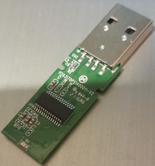
tell me everything you can infer from this image of a busted usb I own.
So the chip appears to have no text on it. That means this is a generic IC/PCB, which doesn't mean the thing is cheap, often the brand name ones use the same.
So that chip up top is the controller. It speaks USB to the computer and it talks to the flash chip(s), which are going to be on the other side. Often the boards are designed to have spots for multiple chips, so they can reuse the same board: the difference between a 32gb drive and a 64gb drive is just how many chips they solder onto it.
So if this thing is dead, it's probably the flash chip. The controllers seem pretty reliable, but they're useless without the flash, and flash chips slowly die as they have a limited number of writes.
And since USB flash drives are effectively disposable, they end up with the cheapest crappiest flash. The good shit goes into enterprise SSDs, then consumer SSDs, then big device on-board-storage (eMMC), then finally SD cards and then USB drives.
So yeah. Can't really tell you anything about it other than that. The numbers you seer are going to be used internally by the PCB assembler, they don't mean anything to anyone else.
147 notes
·
View notes
Text
Printed Circuit Board Basics
Most of us are using Printed Circuit Board in our daily life. Printed Circuit Boards are used in almost all the Electronic products, from consumer gadgets such as PCs, tablets, smartphones, and gaming consoles to industrial and even high tech products in strategic and medical electronics domains.
Here, we have some statistics for you that shows how many electronic devices connect worldwide from 2015 to 2025. This statistic shows an increase in the use of a number of PCB in people daily life. Hence, CircuitWala took this opportunity to provide a basic knowledge about PCB via this article.
There are so many books available online which teach about Printed Circuit Board design and hardware part. There are few links available online which shows only a few basic fundamentals of PCB and few are there for Basics of Printed Circuit Board (PCB) Design. Few which gives good know knowledge on Printed Circuit Board terminology. But in the end for the hobbyist, there is no such material available which make their work easy.
Now days there few online designing websites available which allow hobbyist and students to create their design and Printed Circuit Board fabrication part. These websites provide limited features and charge high for the full edition. We, @CircuitWala are in try to provide one platform which provides plenty of Printed Circuit Board knowledge digitally to make your work simple and easy.
Alternatives of PCB include wire wrap and point-to-point construction. Creating a layout of PCB is a little bit time-consuming method as compared to its alternative solution but manufacturing of PCB is cheaper and faster then other wiring methods as electronic components are mounted and wired with one single part.
Let’s start with some basics of Printed Circuit Board with this article. Here in this article we will discuss about history of PCB to understand the emerge of PCB, Types of PCB to make your complex PCB a very simple using different types, Usage of PCB to provide you an idea to create more Printed Circuit Board projects, Advantages and Disadvantages, Possible Future to know about new technological change in Printed Circuit Board manufacturing and also about how to destroy and manage your PCB’s e-waste? We know you are eager to know all the stuff in details but before that let’s make a simple definition of Printed Circuit Board.
What is Printed Circuit Board?Printed Circuit Board is an electronic device made of conductive material(FR-4) like copper which connects components mounted on it to to get desired output by providing an input on another end.
When the board has not mounted with any of the components is called as Printed Circuit Board or Printed Wired Board. Mounting of an electronic component on Printed Circuit Board is called as PCB assembly.
History of Printed Circuit BoardThe invention of Printed Circuit Board was by Austrian engineer Paul Eisler as part of a radio set while working in England around 1936.
In early days before Printed Circuit Board became common in use, Point-to-Point construction was used. This meant some bulky and unreliable design that required plenty of sockets and regular replacement of it. Most of this issue directly address when PCB went into regular production.
Originally, every electronic component had wire leads, and the PCB had holes drilled for each wire of each component. The components’ leads were then passed through the holes and soldered to the PCB trace. This method of assembly is called Through-Hole construction. There is one other method to mount component is called as Surface Mount.
Type of Printed Circuit BoardPCBs are produced from the different types of material and on the basis of that material PCBs are divided mainly into two parts: Rigid PCB and Flexible PCB. Nowadays, a combination of Rigid and flexible PCB is also possible and that is called as Flexi-Rigid PCBs.
Most of the PCBs are built in layers. The inner layer is the base material called as a substrate. Rigid PCBs are mainly made of material like epoxy materials and Flexible PCBs are made of plastic material that can withstand high temperatures.
Rigid PCBs are generally, hard materials that hold the component in a better way. The motherboard in the tower of a computer is the best example of Rigid PCBs. Flexible PCBs fundamental material allows PCB to fit into forms that Rigid PCBs can not. Flexible PCBs can turn round without harmful the circuit on PCB.
All Rigid and Flexible PCBs can come in three formats by layers: Single Layer, Double Layer, and Multi-Layer.
1. Single Layer PCBSingle Layer PCBs have been around since the late 1950s and still dominate the world market in sheer piece volume. Single Sided PCBs contain only one layer of conductive material and are best suited for low-density designs. Single-sided PCBs are easy to design and quick to manufacture. They serve as the most lucrative platform in the industry.
2. Double Layer PCBDouble Layered printed circuit board technology is conceivably the most popular type of PCB in the industry. Double Sided PCB (also known as Double-Sided Plated Thru or DSPT) circuits are the gateway to advanced technology applications. They allow for a closer (and perhaps more) routing traces by alternating between top and bottom layers using vias.
3. Multi Layer PCB
Multilayer PCB is a circuit board that has more than two layers. Unlike a Double-Sided PCB which only has two conductive layers of material, all multilayer PCBs must have at least three layers of conductive material which are buried in the center of the material.
Usage of Printed Circuit BoardBy reading this article till this point, we hope that you are now able to get about printed circuit boards. Now, we will make you understand about different applications of printed Circuit Board.
In this digital world, Printed Circuit Board is in almost all our daily life electronic devices and in our industrial electronics as well. Below are the industries where PCBs are used:
Possible FutureNowadays, most of the circuits are replaced to produce Printed Circuit Board from the old methods. Revolution in technology made many of the processes automated and hence it is easy to manufacture PCB. But still, these processes are a bit expensive to hire, involve toxic waste and use high temperatures and acids. With technological advances we have seen in the past years, it is not hard to imagine PCB will soon be revolutionized. Not only that but research institutes predict a more ‘green’ future for PCBs; PCBs being made of paper.
Electronic Waste (e-waste)Electronic Waste or e-waste is described as discarded electrical or electronic devices. Informal processing of e-waste in developing countries can lead to adverse human health effects and environmental pollution.
Electronic scrap components contain a hazardous substance such as lead, cadmium, beryllium, or brominated flame retardants. Recycling and disposal of e-waste may involve significant risk to health of workers and communities in developed countries and great care must be taken to avoid unsafe exposure in recycling operations
Nowadays, developing countries are encouraging electronic users to take care while recycling the e-waste or submit them to the organization who are involved in such activities.
SummaryIn this blog, we have learned the basics of Printed Circuit Board. CircuitWala is planning to write as many blogs to provide more and more knowledge of Printed Circuit Board. Either it is basics or manufacturing or usages or advantages and disadvantages of PCBs. We will also try to make our users/customers up to date for the new technology innovations, including past histories and revolution of the PCB industries.
In the next blog, we will look at more briefly about the different types of Printed Circuit Board. We also understand the process to make it and different usage and application for the same.
#electronic circuit design company#pcb circuit manufacturer in ahmedabad#pcb design & manufacturing services#printed circuit board companies#printed circuit board order online#PCB manufacturer#Printed Circuited Board#double layer PCB#PCB Quality Control
2 notes
·
View notes
Text
Pcb Board Terminals Market: Investment Opportunities and Forecast 2025–2032

MARKET INSIGHTS
The global Pcb Board Terminals Market size was valued at US$ 2.67 billion in 2024 and is projected to reach US$ 4.12 billion by 2032, at a CAGR of 5.8% during the forecast period 2025-2032.
PCB board terminals are crucial electrical connectors that facilitate secure and reliable connections between printed circuit boards and external wiring systems. These components come in various types including screw type, plug-in, and other specialized variants, each designed for specific applications across industries. The terminals play a vital role in ensuring proper signal transmission and power distribution in electronic assemblies.
The market growth is driven by several factors, including the expanding electronics manufacturing sector and increasing adoption of automation across industries. The global PCB industry, valued at approximately USD 81 billion in 2022, continues to provide a strong foundation for terminal demand. Emerging technologies like 5G infrastructure, AI hardware, and electric vehicles are creating new opportunities, while established players such as TE Connectivity, WAGO, and Phoenix Contact continue to innovate with compact and high-performance terminal solutions.
MARKET DYNAMICS
MARKET DRIVERS
Expansion of 5G and IoT Infrastructure to Accelerate PCB Terminal Demand
The global rollout of 5G networks and IoT ecosystems is creating unprecedented demand for sophisticated printed circuit boards (PCBs), subsequently driving growth in the PCB terminals market. With over 1.3 billion 5G connections projected worldwide by 2024, network operators are investing heavily in infrastructure that requires high-density interconnect PCBs with reliable terminal connections. These terminals ensure stable signal transmission in base stations and small cell deployments, where vibration resistance and environmental durability are critical. The automotive sector’s shift toward connected vehicles further amplifies this demand, as modern cars now contain 1,500+ PCB terminals for advanced driver-assistance systems (ADAS) and telematics units.
Electrification Wave in Automotive Industry to Fuel Market Expansion
Electric vehicle (EV) production is revolutionizing PCB terminal requirements, with battery management systems (BMS) and power converters requiring specialized high-current terminals. The average EV contains 30% more PCB terminals than conventional vehicles, primarily for managing 400V-800V battery systems. Major manufacturers are responding to this shift – in Q3 2024, TE Connectivity introduced a new line of high-voltage PCB terminals rated for 250A continuous current, addressing the industry’s need for compact yet robust power distribution solutions. This technological evolution coincides with projections that EVs will represent 25% of global auto sales by 2026, creating sustained demand for automotive-grade terminals.
MARKET RESTRAINTS
Raw Material Volatility to Constrain Profit Margins
The PCB terminal market faces significant pressure from fluctuating copper and specialty alloy prices, which account for 60-70% of production costs. Copper prices have shown 22% annual volatility since 2021, forcing manufacturers to either absorb costs or risk losing price-sensitive customers. This challenge is particularly acute in consumer electronics, where terminals represent disposable components in increasingly commoditized devices. The situation is further complicated by geopolitical factors affecting rare earth metal supplies, with certain terminal coatings requiring materials subject to export restrictions.
Miniaturization Challenges to Impact Standard Terminal Designs
As PCBs shrink to accommodate wearable tech and implantable medical devices, traditional screw-type terminals face obsolescence in space-constrained applications. The industry benchmark for terminal pitch has decreased from 5.08mm to 3.5mm in just five years, requiring complete redesigns of insertion and strain relief mechanisms. This transition strains manufacturers’ R&D budgets while simultaneously increasing production complexity – automated assembly systems capable of handling sub-3mm terminals cost 40-50% more than conventional equipment. These technical barriers slow adoption in cost-sensitive market segments.
MARKET CHALLENGES
Legacy System Integration to Create Compatibility Issues
Industrial equipment with lifespans exceeding 15-20 years presents unique challenges for terminal manufacturers. While modern terminals offer superior performance, their mechanical and electrical interfaces often prove incompatible with older PCB designs still prevalent in manufacturing plants. This incompatibility forces end-users into expensive board redesigns or makeshift adapter solutions that compromise reliability – a significant concern in safety-critical applications like power generation. The problem is magnified by the lack of standardization across regional markets, with differing terminal configurations persisting in North America, Europe, and Asia.
MARKET OPPORTUNITIES
Smart Manufacturing Initiatives to Drive Next-Gen Terminal Adoption
Industry 4.0 implementations are creating demand for intelligent terminals with embedded sensors, presenting a $780 million revenue opportunity by 2027. These advanced terminals can monitor connection integrity, temperature, and vibration in real-time, addressing pain points in predictive maintenance programs. Leading suppliers are responding with hybrid solutions – WAGO’s 2024 PRO 2 series combines traditional spring-clamp reliability with IoT connectivity features, demonstrating the market’s direction. The medical equipment sector shows particular promise, where smart terminals could reduce 35% of device failures attributed to connection issues.
Asia-Pacific Infrastructure Boom to Create New Growth Areas
Southeast Asia’s electronics manufacturing expansion represents the most dynamic growth opportunity, with countries like Vietnam and Thailand increasing PCB production capacity by 18-22% annually. Local terminal suppliers benefit from government incentives promoting domestic component sourcing, while global players establish regional technical centers to support just-in-time delivery. This geographical shift complements existing Chinese dominance, where PCB terminal consumption continues growing at 9% CAGR despite economic headwinds. The region’s focus on renewable energy infrastructure further stimulates demand for high-reliability terminals in solar inverters and wind turbine controls.
PCB BOARD TERMINALS MARKET TRENDS
Miniaturization and High-Density PCB Designs Drive Terminal Innovation
A significant trend shaping the PCB terminals market is the increasing demand for compact, high-density solutions due to shrinking electronic device sizes. The global PCB market exceeded $81 billion in 2022, indicating massive production volumes where terminals serve as critical connection points. Manufacturers are responding with ultra-low profile screw-type terminals and micro-plug connectors that maintain reliability while occupying minimal board space. This evolution is particularly crucial for IoT devices and wearables where terminals must accommodate complex circuitry in constrained areas without compromising conductivity or durability.
Other Trends
Electrification of Automotive Systems
The automotive industry’s transition toward electric vehicles (EVs) and advanced driver-assistance systems (ADAS) is creating sustained demand for rugged PCB terminals capable of handling high-voltage applications. EV production is projected to grow at a CAGR of over 23% through 2030, driving innovations in terminals with enhanced vibration resistance and temperature tolerance up to 150°C. These specialized terminals facilitate reliable connections in battery management systems and power distribution units where failure risks must be minimized.
Rise of Automated Manufacturing Processes
The adoption of Industry 4.0 practices is transforming terminal production, with manufacturers integrating automated optical inspection (AOI) systems to ensure micron-level precision in terminal placement. This shift reduces human error while increasing throughput – critical factors as Asian PCB manufacturers now account for over 60% of global production capacity. Furthermore, self-aligning terminal designs are gaining traction for their ability to accelerate robotic assembly processes, particularly in high-volume consumer electronics manufacturing where milliseconds per connection translate directly to cost savings.
COMPETITIVE LANDSCAPE
Key Industry Players
Innovation and Strategic Expansion Drive Market Competition
The PCB board terminals market exhibits a moderately consolidated structure, with prominent players competing alongside emerging regional manufacturers. TE Connectivity leads the global market, commanding a significant share due to its diversified product portfolio and robust distribution network spanning North America, Europe, and Asia-Pacific. The company’s focus on high-reliability connectors for automotive and industrial applications has reinforced its market position.
Other major players such as WAGO and Phoenix Contact have strengthened their foothold through continuous technological advancements in screw-type and plug-in terminals. These companies benefit from strong R&D capabilities and strategic partnerships with PCB manufacturers across various end-use sectors.
Meanwhile, Asian manufacturers like OMRON and Amphenol are rapidly gaining traction, supported by the region’s thriving electronics manufacturing ecosystem. These players are investing heavily in compact, high-density terminal solutions to meet the increasing demand from consumer electronics and telecommunications sectors.
The competitive intensity is further amplified by mid-sized specialists such as Weidmüller and Wieland Electric who are carving out niche positions through customized solutions for industrial automation applications. Recent acquisitions and vertical integration strategies among these players indicate a shifting competitive dynamic that prioritizes both product performance and supply chain efficiency.
List of Key PCB Board Terminal Companies Profiled
TE Connectivity (Switzerland)
WAGO (Germany)
Altech Chemicals (U.S.)
Weidmüller (Germany)
Phoenix Contact (Germany)
WECO Electrical Connectors (U.S.)
DINTEK (Taiwan)
ABB (Switzerland)
Essen Deinki (China)
Wieland Electric (Germany)
OMRON (Japan)
Molex (U.S.)
Amphenol (U.S.)
Segment Analysis:
By Type
Screw Type Terminals Lead the Market Due to Superior Connectivity and Durability
The PCB board terminals market is segmented based on type into:
Screw Type
Subtypes: Spring-loaded, through-hole, and others
Plug-In
Subtypes: Push-in, spring-clamp, and others
Other Types
Subtypes: Barrier strips, IDC connectors, and others
By Application
Electronic Products Segment Dominates Owing to Proliferation of Consumer Electronics
The market is segmented based on application into:
Electronic Products
Automotive Equipment
Bathroom Equipment
Industrial Machinery
Medical Devices
By End User
Automotive Sector Shows Fastest Growth Due to Increasing Vehicle Electrification
The market is segmented by end user into:
Consumer Electronics Manufacturers
Automotive OEMs
Industrial Equipment Manufacturers
Medical Device Companies
Telecommunication Providers
By Material
Copper Alloys Remain Preferred Choice for Optimal Conductivity and Cost-Effectiveness
The market is segmented by material type into:
Copper Alloys
Subtypes: Brass, phosphor bronze, and others
Aluminum
Nickel Alloys
Other Materials
Regional Analysis: PCB Board Terminals Market
North America The North American PCB board terminals market is characterized by high-tech adoption and stringent quality standards. The U.S. holds the largest share, driven by strong demand from the electronics and automotive sectors, where PCB terminals are critical for secure connections in circuit boards. The region benefits from advanced manufacturing capabilities, particularly in AI hardware, 5G infrastructure, and electric vehicle (EV) components. While environmental regulations influence material choices, the focus remains on high-performance terminals that meet safety and durability criteria. Major players like TE Connectivity and Amphenol dominate supply chains, supporting innovation in miniaturized and high-current terminals.
Europe Europe’s market thrives on industrial automation and renewable energy projects, which demand reliable PCB terminals for control systems and power distribution. Germany leads in manufacturing, with companies like WAGO and Phoenix Contact supplying screw-type and plug-in terminals for automotive and industrial applications. The EU’s circular economy policies encourage recyclable materials, pushing vendors to adopt sustainable designs. However, higher production costs and competition from Asian imports challenge local suppliers. Despite this, the region maintains a niche in precision-engineered solutions, especially for medical devices and aerospace.
Asia-Pacific As the largest and fastest-growing market, APAC accounts for over 60% of global PCB production, with China, Japan, and South Korea as key hubs. The boom in consumer electronics, EVs, and IoT devices fuels demand for cost-effective terminals, favoring plug-in variants. China’s local manufacturers leverage economies of scale, though quality disparities exist. Japan and South Korea excel in high-density terminals for advanced applications, driven by companies like OMRON and Molex. While price sensitivity limits premium product adoption, urbanization and 5G rollout offer long-term growth opportunities across the region.
South America South America’s market is nascent but evolving, with Brazil and Argentina leading demand for PCB terminals in automotive and appliance manufacturing. Economic instability and reliance on imports hinder local production, but government incentives for electronics industrialization are gradually attracting investments. The lack of strict standards results in a mix of low-cost imports and niche domestic offerings. However, the rise of renewable energy projects and smart infrastructure could drive future demand for durable terminal solutions.
Middle East & Africa MEA shows moderate growth, primarily in GCC countries like the UAE and Saudi Arabia, where PCB terminals are used in oil & gas automation and construction technologies. Limited local manufacturing forces dependence on imports, though initiatives like Saudi Vision 2030 aim to boost electronics self-sufficiency. Africa’s market remains fragmented, with South Africa leading in industrialapplications, while other regions face challenges like infrastructure gaps and low purchasing power. Nonetheless, urbanization and digitalization trends hint at untapped potential.
Report Scope
This market research report provides a comprehensive analysis of the global and regional PCB Board Terminals markets, covering the forecast period 2025–2032. It offers detailed insights into market dynamics, technological advancements, competitive landscape, and key trends shaping the industry.
Key focus areas of the report include:
Market Size & Forecast: Historical data and future projections for revenue, unit shipments, and market value across major regions and segments. The global PCB Board Terminals market was valued at USD 2.8 billion in 2024 and is projected to reach USD 4.1 billion by 2032, growing at a CAGR of 4.7%.
Segmentation Analysis: Detailed breakdown by product type (Screw Type, Plug-In, Others), application (Electronic Products, Automotive Equipment, Bathroom Equipment), and end-user industry to identify high-growth segments.
Regional Outlook: Insights into market performance across North America, Europe, Asia-Pacific, Latin America, and Middle East & Africa. Asia-Pacific dominates with 62% market share in 2024.
Competitive Landscape: Profiles of 13 leading market participants including TE Connectivity, WAGO, and Phoenix Contact, with their product portfolios, market shares, and strategic developments.
Technology Trends & Innovation: Assessment of emerging trends like miniaturization, high-current terminals, and smart connectivity solutions in PCB terminals.
Market Drivers & Restraints: Evaluation of factors including 5G deployment, EV adoption, and industrial automation driving growth, along with raw material price volatility challenges.
Stakeholder Analysis: Strategic insights for PCB manufacturers, terminal suppliers, OEMs, and investors regarding market opportunities and competitive positioning.
Related Reports:https://semiconductorblogs21.blogspot.com/2025/06/inductive-proximity-switches-market.htmlhttps://semiconductorblogs21.blogspot.com/2025/06/cellular-iot-module-chipset-market.htmlhttps://semiconductorblogs21.blogspot.com/2025/06/sine-wave-inverter-market-shifts-in.htmlhttps://semiconductorblogs21.blogspot.com/2025/06/pilot-air-control-valves-market-cost.htmlhttps://semiconductorblogs21.blogspot.com/2025/06/video-multiplexer-market-role-in.htmlhttps://semiconductorblogs21.blogspot.com/2025/06/semiconductor-packaging-capillary.htmlhttps://semiconductorblogs21.blogspot.com/2025/06/screw-in-circuit-board-connector-market.htmlhttps://semiconductorblogs21.blogspot.com/2025/06/wafer-carrier-tray-market-integration.htmlhttps://semiconductorblogs21.blogspot.com/2025/06/digital-display-potentiometer-market.htmlhttps://semiconductorblogs21.blogspot.com/2025/06/glass-encapsulated-ntc-thermistor.htmlhttps://semiconductorblogs21.blogspot.com/2025/06/shafted-hall-effect-sensors-market.htmlhttps://semiconductorblogs21.blogspot.com/2025/06/point-of-load-power-chip-market.htmlhttps://semiconductorblogs21.blogspot.com/2025/06/x-ray-grating-market-key-players-and.htmlhttps://semiconductorblogs21.blogspot.com/2025/06/picmg-single-board-computer-market.htmlhttps://semiconductorblogs21.blogspot.com/2025/06/lighting-control-dimming-panel-market.html
0 notes
Text
Organized Precision: High-Quality PCB Magazine Rack in India – Only at Ascomp Inc
When handling delicate printed circuit boards (PCBs), proper storage and handling are critical to prevent physical damage, static discharge, and contamination. In production lines, testing labs, and assembly units, using a reliable PCB magazine rack in India ensures safe transport, handling, and storage of PCBs without compromising quality or efficiency. At Ascomp Inc, we offer a wide range of robust and anti-static PCB racks, designed for industrial use and optimized for Indian manufacturing environments.
What is a PCB Magazine Rack?
A PCB magazine rack is a specialized storage unit designed to hold multiple PCBs vertically or horizontally. Made from heat-resistant and ESD-safe materials like conductive plastic or aluminum alloy, these racks protect PCBs during handling, transit, and storage. They are commonly used in:
SMT lines
Assembly and inspection workstations
Wave soldering and reflow zones
Testing and quality control areas
Each PCB magazine rack in India from Ascomp Inc is built to ensure mechanical stability, cleanroom compatibility, and anti-static protection.
Features of Ascomp Inc’s PCB Racks
✅ Adjustable slot width to accommodate different PCB sizes
✅ Stackable and lightweight design for space efficiency
✅ Durable, ESD-safe materials to prevent static damage
✅ Heat-resistant structure for high-temp production areas
✅ Models with rollers for easy mobility between lines
✅ Locking mechanisms to keep PCBs securely in place
Our racks are compatible with both manual handling and robotic automation systems used in advanced SMT and EMS setups.
Applications Across Industries
Ascomp Inc supplies PCB magazine racks to industries such as:
Electronics manufacturing and SMT assembly
Automotive electronics and EV units
Aerospace and defense electronics labs
Medical device and telecom PCB fabrication
R&D labs and prototyping facilities
Consumer electronics repair and refurbishment hubs
We help companies ensure that PCBs move through the production lifecycle with safety, efficiency, and traceability.
Customization Options
Different PCB sizes and handling requirements call for tailored solutions. That’s why Ascomp Inc offers:
Adjustable rack models for varying board thickness
Horizontal and vertical slot orientations
Customized branding and labeling
Options with antistatic wheels and handles
Cleanroom-grade builds upon request
We also provide full technical guidance to select the right rack model based on your product mix and workflow.
Why Choose Ascomp Inc?
🧰 Experienced supplier of ESD and assembly accessories
📦 PAN-India delivery and fast fulfillment for bulk orders
🛠️ Durable and industry-tested products
📞 Dedicated support for technical queries and custom needs
💼 Trusted by EMS, OEM, and R&D labs across India
We are committed to supporting India’s growing electronics ecosystem with the infrastructure it needs to scale safely and efficiently.
#PCBMagazineRackIndia#AscompInc#ESDStorageIndia#ElectronicsManufacturingTools#PCBHandlingIndia#SMTAssemblyTools#CleanroomStorage#AntiStaticRacks#PCBProductionIndia#IndustrialStorageSolutions
0 notes
Text
Top 10 Electronics Manufacturing Companies in India You Should Know About
India is rapidly becoming a global hotspot for electronics manufacturing, and it’s no accident. Thanks to government initiatives like Make in India and PLI (Production Linked Incentive), along with a skilled workforce and cost-competitive production, electronics manufacturing companies in India are shaping the future of global tech.
If you’re in the electronics industry or simply curious about the powerhouses driving India’s growth, here’s a curated list of the Top 10 Electronics Manufacturing Companies in India you should have on your radar.
Let’s dive in.
Why India for Electronics Manufacturing?
✅ Skilled Workforce: Thousands of engineers entering the industry every year.
✅ Policy Support: Incentives through Make in India & PLI schemes.
✅ Global Demand: Supplying top brands worldwide.
✅ Innovation Focus: Companies invest heavily in R&D for future technologies.
⚙️ Top 10 Electronics Manufacturing Companies in India
1️⃣ Dixon Technologies
Noida-based Dixon Technologies leads the way in contract manufacturing for electronics. They work with major global brands producing everything from smartphones to LED TVs.
Specialties:
Consumer Electronics
Mobile Phones
Lighting & Security Devices
Why Dixon? Trusted by names like Samsung, Xiaomi & Panasonic.
2️⃣ Bharat Electronics Limited (BEL)
A government-owned giant, BEL is best known for defense electronics but also manufactures products for telecom, civilian, and broadcast sectors.
Specialties:
Defense Electronics
Communication Equipment
Radar Systems
Why BEL? Top choice for mission-critical and defense-grade tech.
3️⃣ Elin Electronics
Based in Ghaziabad, Elin Electronics provides EMS solutions across LED lighting, appliances, and medical devices.
Specialties:
PCBA
Small Appliances
Automotive Electronics
Why Elin? Known for quality and reliable partnerships.
4️⃣ Syrma SGS Technology
Catering to IoT, automotive, and healthcare industries, Syrma SGS stands out for both manufacturing and design services.
Specialties:
Electronics Manufacturing
RFID
Custom Magnetics
Why Syrma? Global clientele and versatile capabilities.
5️⃣ Avalon Technologies
With a focus on high-complexity assemblies, Avalon is ideal for companies needing precision engineering and system integration.
Specialties:
PCB Assembly
System Integration
Cable Assemblies
Why Avalon? Perfect for custom, small-batch production.
6️⃣ SFO Technologies (NeST Group)
A key player for companies in aerospace, healthcare, and industrial automation, SFO Technologies delivers more than just manufacturing—they build complete systems.
Specialties:
EMS
Embedded Systems
Software Development
Why SFO? Seamless integration of software and hardware expertise.
7️⃣ Kaynes Technology
If you’re in the IoT game, Kaynes Technology is a name to remember. They offer end-to-end EMS services, especially for IoT, automotive, and defense.
Specialties:
IoT Product Development
Embedded Systems
Automotive Electronics
Why Kaynes? Known for cutting-edge innovation in connected tech.
8️⃣ Optiemus Electronics Limited (OEL)
A major contributor to India’s smartphone manufacturing revolution, OEL partners with global brands to build mobile devices and accessories.
Specialties:
Mobile Phones
Wearables
Accessories
Why Optiemus? Trusted by telecom giants for device manufacturing.
9️⃣ VVDN Technologies
What sets VVDN apart is their design-led manufacturing approach, especially for IoT, telecom, and networking solutions.
Specialties:
IoT Product Design
Embedded Software
Cloud & App Integration
Why VVDN? Full-stack development plus manufacturing.
🔟 Centum Electronics
For high-reliability electronics in critical sectors like space and defense, Centum Electronics is a leader, supplying even ISRO and DRDO.
Specialties:
Aerospace Electronics
Microelectronics
Defense Tech
Why Centum? Precision-built for mission-critical applications.
🏆 How to Choose Your Manufacturing Partner?
Here’s what you should focus on when selecting an electronics manufacturing company:
✔ Industry Expertise
✔ Certifications (ISO, IATF, etc.)
✔ Capacity for Production Scale
✔ Design & R&D Capabilities
✔ Location and Logistics
Pro Tip: Use platforms like FindingMFG to connect with verified manufacturers across India. It’s faster, safer, and saves a lot of hassle.
🌐 Ready to Start?
The electronics manufacturing company in India is growing stronger every year—and these companies are leading the charge. Whether you’re launching a startup, scaling your supply chain, or just exploring opportunities in tech manufacturing, India’s EMS ecosystem has the solutions you need.
👉 Explore more at FindingMFG.com
#electronics manufacturing#electronics manufacturing companies#top 10 electronics manufacturing companies in India#manufacturing directory#business directory
0 notes
Text
PCBA: The Silent Backbone of Electronic Devices
Printed Circuit Board Assembly (PCBA) serves as the critical foundation for nearly every electronic device in our modern world. From smartphones and laptops to industrial automation systems and aerospace equipment, PCBA ensures that the various electronic components within a device function smoothly and cohesively. Its precision and reliability are not just technical necessities but vital to sustaining innovation in the global tech economy.Get more news about PCBA manufacturer,you can vist our website!
Understanding PCBA
At its core, PCBA refers to the process of soldering electronic components onto a printed circuit board (PCB). While a PCB is simply the board with copper traces that connect components electrically, the assembly process transforms it into a fully functional circuit. This involves mounting integrated circuits (ICs), resistors, capacitors, diodes, and other components using either Surface Mount Technology (SMT), Through-Hole Technology (THT), or a hybrid of both, depending on the design and purpose of the device.
The PCBA Process
The process typically begins with solder paste application, where a stencil is used to apply the paste on predefined areas of the PCB. Automated pick-and-place machines then accurately position the tiny components onto the board. This is followed by reflow soldering, where the board is passed through a controlled oven to melt the solder and secure the components.
For boards requiring through-hole components, manual or wave soldering is used. Once soldered, the board undergoes inspection and testing—ranging from Automated Optical Inspection (AOI) to X-ray analysis and functional testing—to ensure quality and performance. Advanced PCBA plants employ high levels of automation, drastically reducing human error and improving output consistency.
Applications Across Industries
PCBA's influence stretches far beyond consumer electronics. In the automotive sector, it powers systems ranging from infotainment units to electric vehicle battery management. In healthcare, PCBA-based medical devices like ECG machines and portable monitors are critical to patient diagnostics and care. Aerospace and military applications demand high-reliability PCBA to function under extreme environments—an area where rigid quality controls and testing standards become indispensable.
Trends and Innovations
The PCBA landscape continues to evolve rapidly with advances in miniaturization, multi-layer boards, and flexible circuits. With the rise of the Internet of Things (IoT), demand for compact, power-efficient, and wireless-capable assemblies has exploded. Manufacturers are investing in smart factories, using AI-driven inspection and robotics to further optimize production.
Meanwhile, environmental considerations are pushing green manufacturing methods, such as lead-free solder and recyclable board materials. Companies are also embracing design-for-manufacturing (DFM) principles to streamline assembly and minimize waste.
Conclusion
Though rarely visible to end-users, PCBA is the invisible force driving the electronics revolution. Its blend of engineering precision, automation, and innovation enables the digital tools and systems we rely on daily. As global technology continues to push boundaries, PCBA will remain the structural and functional heart of that progress—quietly pulsing behind every screen, circuit, and sensor.
0 notes
Text
Choosing the Right Electronics Manufacturing Services Provider in India: What You Need to Know
The electronics industry is witnessing exponential growth, driven by rising global demand for smart devices, IoT integration, and automation. In this dynamic landscape, partnering with a reliable Electronics Manufacturing Services Provider in India has become a strategic necessity for companies aiming to scale production, improve quality, and reduce time-to-market.
India, emerging as a global hub for electronics manufacturing, provides a cost-effective and quality-focused environment for Original Equipment Manufacturers (OEMs) across various sectors, including consumer electronics, automotive, and industrial applications. If you're a business looking to collaborate with a top-tier electronics manufacturing services provider in India, understanding what to look for and how the right EMS partner can support your growth is essential.
What Are Electronics Manufacturing Services?
Electronics Manufacturing Services (EMS) refer to companies that design, manufacture, test, distribute, and provide return and repair services for electronic components and assemblies. These providers are key partners for OEMs who prefer to outsource manufacturing to experts rather than maintain in-house capabilities. An EMS partner typically offers:
- PCB (Printed Circuit Board) assembly
- Surface Mount Technology (SMT) and Through-Hole assembly
- Prototyping and NPI (New Product Introduction) support
- Functional and in-circuit testing
- Box build and final system integration
- Supply chain management
- Aftermarket support and logistics
Why Choose an EMS Provider in India?
India is rapidly climbing the ranks as a preferred destination for electronics manufacturing due to several favorable factors:
1) Cost-Effectiveness: Manufacturing in India offers significant cost savings without compromising on quality. Lower labor costs, competitive overheads, and government-backed subsidies help original equipment manufacturers (OEMs) remain profitable.
2) Government Incentives: Under the “Make in India” initiative and Production Linked Incentive (PLI) schemes, EMS providers in India receive various tax incentives, subsidies, and support that help reduce total manufacturing costs for OEMs.
3) Skilled Workforce: India has a large, educated, and technically proficient workforce, especially in areas such as PCB assembly, quality assurance, and embedded system development.
4) Strategic Location: With its proximity to global markets in Asia, Europe, and the Middle East, India serves as a logistics hub, boasting strong port infrastructure and connectivity.
Key Advantages of Partnering with an EMS Provider
Partnering with an EMS provider isn’t just about outsourcing production; it’s about building a long-term relationship that enhances your competitiveness and operational efficiency. Here’s how:
1) Faster Time-to-Market: An experienced EMS provider can expedite design iterations, prototyping, and mass production, thereby reducing the time required to bring new products to market.
2) Quality Control: Top EMS companies adhere to global standards, including ISO 9001, IATF 16949, and IPC-A-610, for electronics assembly and testing, ensuring high-quality, defect-free output.
3) Scalability: Whether you’re launching a niche product or scaling up to millions of units, EMS partners provide the flexibility to adjust production volumes efficiently.
4) Focus on Core Competencies: Outsourcing manufacturing enables OEMs to focus on design, innovation, marketing, and customer experience while their EMS partner handles operations and fulfillment.
5) Integrated Supply Chain: With robust procurement capabilities and established vendor relationships, EMS providers help mitigate risks associated with component shortages, cost volatility, and logistics challenges.
What to Look for in an Electronics Manufacturing Services Provider in India
Not all EMS companies offer the same capabilities. When evaluating an EMS provider, consider the following:
1) End-to-End Capabilities: Choose a provider that can support your product lifecycle—from prototyping and low-volume builds to high-volume production and post-sales support.
2) Industry Experience: Look for providers with proven experience in your specific industry, whether it’s medical devices, automotive electronics, consumer goods, or industrial controls.
3) Quality Certifications: Ensure they meet global quality and safety standards, such as ISO, RoHS, and IPC compliance. These standards reflect a commitment to performance, safety, and environmental responsibility.
4) Engineering Support: Strong design-for-manufacturability (DFM) and design-for-testability (DFT) expertise ensure fewer production errors and reduced costs.
5) Communication & Project Management: A transparent approach to communication, real-time reporting, and dedicated account managers ensure that your projects stay on track.
Resolute Electronics: A Trusted EMS Partner in India
One EMS provider that stands out in India’s manufacturing ecosystem is Resolute Electronics, a company known for its customer-first approach and robust capabilities. With state-of-the-art infrastructure, skilled engineers, and a commitment to quality, Resolute has established itself as a trusted provider of electronics manufacturing services in India, serving both global and domestic Original Equipment Manufacturers (OEMs). Their service offerings include:
- Advanced SMT lines for high-speed PCB assembly
- Precision testing with automated optical inspection (AOI), ICT, and functional test setups
- Comprehensive prototyping and NPI support
- Custom enclosures and complete box builds
- Scalable manufacturing solutions for startups to enterprise-level companies
Resolute Electronics also stands out for its flexibility, attention to detail, and ability to bring complex product ideas to life, making it an ideal partner for companies looking to outsource manufacturing without compromising control or visibility.
The Future of EMS in India
As global brands seek to diversify their supply chains and reduce dependence on single-region sourcing, India is poised to play a more significant role in global electronics production. The country’s EMS sector is expected to experience rapid growth over the next decade, driven by both domestic demand and export potential.
With this evolution, OEMs have a unique opportunity to collaborate with EMS partners like Resolute Electronics, who combine technical excellence, responsive service, and innovation to drive business growth.
Conclusion
The right electronics manufacturing services provider in India can be a game-changer for your business, enhancing product quality, reducing costs, and speeding up your time to market. As the demand for smart, connected devices grows, choosing an EMS partner with proven expertise, state-of-the-art facilities, and a flexible engagement model will position your brand for long-term success. Whether you're a startup looking to bring your first product to life or a global brand aiming to scale efficiently, partnering with an EMS provider like Resolute Electronics ensures your electronics manufacturing needs are in expert hands.
0 notes
Text
Electronics Manufacturing: Trends and Industry Insights


In an industry defined by continuous development and exacting standards, electronics manufacturing is a critical driver of modern technology. From everyday consumer goods to complex industrial systems, the journey of each component begins with thoughtful engineering, rigorous production practices, and strong supplier relationships. Based in Arundel, West Sussex, Arrival Electronics Limited stands at the heart of this field, working closely with clients to meet the evolving needs of today’s electronic markets.
This article explores the inner workings of the electronic components industry—what drives it, the trends shaping it, and what decision-makers should understand when choosing the right components or partners. Whether you're a design engineer, purchasing manager, or systems integrator, a clear understanding of this sector will help support better outcomes for your business and your customers.
Understanding the Electronics Manufacturing Process
The process involves assembling electronic components into complete, functional products ready for use or distribution. This can include simple printed circuit board assemblies or more intricate systems involving hundreds of interconnected parts. The process demands consistent quality, traceability, and efficient logistics from start to finish.
The primary stages include:
Component Sourcing: Reliable supply chains and vetted manufacturers are essential. Components must meet specifications, often under strict time constraints and regulatory compliance requirements.
PCB Assembly: Surface mount technology (SMT) and through-hole assembly are key methods used in creating circuit boards. Attention to detail is vital here, as even minor errors can result in failure during testing or deployment.
Testing and Inspection: Functional tests, visual inspections, and X-ray analysis are just some of the methods used to confirm product reliability. These steps help ensure products perform as intended once installed.
Final Assembly and Packaging: After testing, products are assembled into enclosures, labeled, and prepared for shipment, often requiring anti-static handling, thermal protection, or precise labeling practices.
Producing electronic products requires more than tools and machines—it’s about consistency, communication, and adapting to specific project demands.
Key Trends Shaping Today’s Production Landscape
As technology progresses, the electronics sector must constantly adjust. Here are several trends affecting the direction of the industry:
1. Miniaturization
Devices are shrinking, but performance expectations remain high. Engineers must work with tighter tolerances and more complex component configurations. This puts pressure on design and manufacturing teams to align on specifications early in the project lifecycle.
2. Demand for Custom Solutions
Many industries—such as medical, aerospace, and renewable energy—are looking for specialized circuit designs rather than one-size-fits-all solutions. Manufacturers that can provide flexible production runs, in-depth technical consultation, and fast turnarounds are in demand.
3. Supply Chain Resilience
The global component shortage has made it clear how critical supply chain visibility and reliability are. Businesses are increasingly working with sourcing partners that can offer a wide selection of inventory, cross-reference alternatives, and reduce exposure to delays.
4. Sustainability in Manufacturing
There is growing interest in sustainable production practices, including RoHS compliance, lead-free soldering, and energy-efficient factory environments. Electronics manufacturers must respond by implementing responsible processes and working with suppliers who share the same values.
Why Quality and Compliance Matter More Than Ever
When it comes to production and assembly, quality is more than a buzzword—it's a measurable requirement. A faulty capacitor or misaligned connector can result in expensive system failures, regulatory issues, or even safety concerns.
To meet modern expectations, manufacturers must:
Follow ISO-certified procedures
Maintain full traceability of components
Ensure regulatory compliance across target markets (CE, UL, REACH, etc.)
Maintain strong documentation for every stage of the process
Choosing a manufacturing partner with a deep understanding of international standards and a history of consistent delivery helps reduce risks and keeps projects on track.

What Sets Our Manufacturing Services Apart
Our approach is built around delivering practical, cost-effective manufacturing solutions tailored to meet each customer’s unique requirements. By applying lean manufacturing principles, we help clients reduce waste, improve efficiency, and gain measurable value in every step of the process.
Key benefits include:
Lower inventory demands
Reduced total acquisition costs
Supply chain resilience through multiple inventory locations
Improved product quality
Consistent, on-time delivery you can rely on
What to Consider When Choosing a Technical Assembly Partner
Finding a reliable service provider is about more than pricing or proximity. Here are key factors to evaluate:
1. Technical Expertise
Look for teams that can interpret your bill of materials (BOM), understand the application of each component, and make suggestions where appropriate. This ensures that your products are not only assembled correctly but also designed for success.
2. Supplier Relationships
Does the provider have access to a wide range of reputable manufacturers? Can they offer alternatives when primary parts are unavailable? These questions are especially important during global shortages or when dealing with niche specifications.
3. Project Flexibility
Can they accommodate small production runs or prototype builds? Can they ramp up to meet large-scale demand? Flexibility ensures that your partner can adjust alongside your project’s lifecycle.
4. Transparent Communication
Regular updates, clear technical feedback, and documentation of every phase help create confidence. Projects that lack open communication are more likely to experience delays and misunderstandings.
5. End-to-End Support
From early-stage design reviews to post-sale technical queries, the most reliable firms remain actively involved throughout the entire process. They provide ongoing value and ensure long-term reliability, not just short-term assembly.
Meeting Industry Demands: A Practical Approach
The sector serves a wide range of industries, including automotive, medical, aerospace, defense, consumer goods, and industrial automation.. Each sector has its own regulatory environment, tolerances, and expectations for delivery timeframes.
For instance:
Medical devices often require cleanroom assembly and documentation to meet stringent approval standards.
Automotive components must withstand harsh environmental conditions and vibration without performance degradation.
Aerospace systems demand redundancy, traceability, and exact part performance for mission-critical applications.
As these requirements grow more complex, manufacturing partners must respond with tailored approaches—balancing engineering support, materials expertise, and practical experience.
Building Long-Term Success with Trusted Partners
Supply chain challenges, new materials, evolving regulations—these realities require ongoing adaptation. Companies that treat production as a strategic function rather than a transactional service gain a competitive edge.
To succeed, it's essential to work with a partner that:
Understands your industry
Invests in continuous improvement
Keeps up with changing compliance rules
Prioritizes reliability over shortcuts
This is where experience matters. Businesses with a consistent record of on-time delivery, error-free builds, and in-depth component knowledge provide a firm foundation for long-term growth.
About Arrival Electronics Limited
Located in West Sussex, Arrival Electronics Limited is an independent electronic component supplier with deep roots in the electronics manufacturing sector. Known for its technical approach, reliable stock availability, and excellent customer support, the company serves clients across a wide range of industries—including automotive, broadcast, industrial, and aerospace.
Their team offers more than just product sourcing—they offer insight. They collaborate with manufacturers and design engineers to ensure all supplied parts meet application-specific needs. Whether supporting high-mix production or long-term component supply, Arrival Electronics Limited provides dependable service and extensive market knowledge that adds lasting value.
Final Thoughts
Electronics manufacturing is not just a mechanical process; it's a critical function that supports the quality, safety, and performance of the technology we depend on every day. Businesses that understand its nuances are better positioned to deliver products that work as intended, meet compliance goals, and perform reliably over time.
For companies seeking support in this complex space, Arrival Electronics Limited stands as a resourceful and experienced partner. With technical insight, customer dedication, and a clear understanding of today’s component landscape, they help businesses navigate the challenges and practical realities of bringing modern electronic products to market.
0 notes
Text
Boost SMT Quality with Automated Optical Inspection
Surface Mount Technology (SMT) has become the backbone of modern electronics manufacturing. As circuit boards grow more complex and component sizes continue to shrink, maintaining production quality has become more challenging. To address this, manufacturers rely on SMT automated optical inspection systems to enhance efficiency and ensure product reliability.
What Is SMT Automated Optical Inspection?
SMT automated optical inspection (AOI) is a high-speed visual inspection process used to verify the placement, alignment, and soldering of components on a printed circuit board (PCB). Using high-resolution cameras and advanced image processing algorithms, AOI systems scan each board for potential defects during or after assembly.
By catching issues early, these systems reduce rework, prevent defective units from moving forward, and increase yield rates. AOI is typically deployed at multiple points in the production line, including:
Post-solder paste inspection
Pre-reflow inspection
Post-reflow inspection
Each inspection stage targets specific issues such as insufficient solder, component misalignment, or solder bridging.
Why SMT AOI Is Critical to Electronics Manufacturing
The electronics industry demands tight tolerances and minimal defect rates. Even a single misplaced component can lead to product failure. Here's how SMT automated optical inspection supports manufacturing excellence:
1. Enhanced Accuracy
Automated inspection provides greater consistency than manual methods. It can detect:
Incorrect component orientation
Missing components
Cold solder joints
Tombstoning and lifted leads
These defects are often too subtle or time-consuming to spot with manual inspection.
2. Real-Time Feedback
Modern AOI systems integrate seamlessly into SMT lines, providing real-time defect detection and process feedback. When an issue is identified, operators receive alerts to make immediate adjustments. This minimizes downtime and material waste.
3. Scalable Performance
As demand increases, manual inspection becomes a bottleneck. AOI systems handle high-speed production environments with ease, inspecting hundreds of boards per hour without sacrificing accuracy. This makes SMT automated optical inspection ideal for both high-volume and high-mix production lines.
Benefits of Implementing AOI in SMT Production
Investing in AOI provides a range of tangible benefits:
Improved Product Quality: Early detection leads to fewer returns and better customer satisfaction.
Lower Operational Costs: Reducing scrap and rework translates to cost savings.
Faster Time to Market: Streamlined inspection accelerates the production cycle.
Compliance and Traceability: AOI systems often include data logging and defect classification features, aiding in quality audits and process optimization.
Common Defects Detected by SMT AOI
Effective inspection covers a wide array of potential issues, including:
Component misplacement
Solder bridges
Open circuits
Polarity errors
Solder balling
Insufficient or excessive solder
With high-resolution imaging and intelligent algorithms, AOI tools identify and classify these defects rapidly and with minimal human oversight.
Integrating AOI with Other SMT Equipment
For optimal results, AOI should be part of a fully integrated SMT inspection strategy. When combined with solder paste inspection (SPI) and X-ray inspection, manufacturers gain a full view of the assembly process. This layered approach ensures each stage is validated before moving to the next.
For instance, SPI evaluates solder paste deposition before components are placed, while AOI checks component placement and solder joints. In cases where defects may be hidden (like under BGAs), X-ray inspection complements AOI to provide a complete defect profile.
Choosing the Right AOI System
Selecting an appropriate AOI solution depends on several factors:
Board complexity
Component density
Production volume
Required inspection speed
Advanced AOI systems offer features such as 3D imaging, machine learning algorithms, and intuitive software interfaces. These innovations reduce false calls, simplify programming, and improve inspection reliability.
To explore AOI systems designed specifically for SMT applications, visit ASC International. Their cutting-edge technology supports manufacturers looking to improve inspection accuracy and throughput.
Final Thoughts
As electronics manufacturing grows more demanding, quality assurance tools must keep pace. SMT automated optical inspection provides the speed, accuracy, and consistency needed to meet today’s rigorous production standards. By identifying defects early and ensuring high-quality output, AOI protects your bottom line and strengthens customer confidence.
0 notes
Text
Why Are Surface Mount Inductors Vital in Modern Electronics? A Complete Guide

Surface mount inductors have emerged as critical components in today’s compact and high-performance electronic devices. As the demand for miniaturization and efficiency continues to grow, these components offer a reliable solution for energy storage, filtering, and signal integrity. Whether you are designing consumer electronics, industrial systems, or automotive applications, understanding the role and advantages of surface mount inductors can significantly enhance your product development process.
What Are Surface Mount Inductors?
Surface mount inductors are passive electronic components designed to store energy in a magnetic field when electrical current flows through them. Unlike traditional through-hole inductors, surface mount variants are mounted directly onto the surface of a printed circuit board (PCB), enabling compact, low-profile, and automated assembly designs. These inductors are widely used for their efficient space utilization and high-frequency performance.
How Do Surface Mount Inductors Work?
The basic working principle of surface mount inductors is grounded in electromagnetic induction. When current passes through the coil inside the inductor, it creates a magnetic field. This field resists changes in the current, providing a filtering or energy storage function depending on the application.
Surface mount inductors are typically manufactured using a ferrite or powdered iron core surrounded by a coiled conductor. The magnetic properties of the core and the number of coil turns determine the inductance value. Their compact design allows them to perform reliably in dense circuit boards.
Where Are Surface Mount Inductors Used?
These inductors are essential in multiple sectors where space-saving components are crucial. Common applications include:
Smartphones, tablets, and laptops
Power supplies and DC-DC converters
Automotive electronic control units (ECUs)
RF and telecommunications systems
Medical and industrial instrumentation
LED lighting systems and IoT modules
Each of these areas requires high-performance signal integrity and energy efficiency, both of which are facilitated by surface mount inductors.
What Are the Key Benefits of Surface Mount Inductors?
Surface mount inductors provide a range of advantages for engineers and product designers. Their integration into compact electronics is particularly valuable in today’s market.
Enable miniaturized circuit design for compact devices
Support high-frequency operations with excellent performance
Reduce production time through automated pick-and-place mounting
Offer low DC resistance (DCR) for higher efficiency
Enhance electromagnetic compatibility (EMC) in sensitive circuits
Provide thermal stability in harsh environments
Available in a wide variety of inductance values and sizes
These benefits make them indispensable in both analog and digital electronic systems.
What Are the Different Types of Surface Mount Inductors?
The choice of surface mount inductor depends on the specific application and performance requirements. Key types include:
Wire-wound inductors: Known for high Q-factor and current handling capabilities, ideal for power applications.
Multilayer inductors: Offer compact size and are suitable for high-frequency filtering.
Thin-film inductors: Deliver precision and low-profile characteristics, often used in RF circuits.
Molded inductors: Provide strong mechanical durability, often used in automotive environments.
Each type has unique characteristics that influence its behavior in a circuit, and selecting the right one depends on factors such as frequency, current rating, and size constraints.
How to Choose the Right Surface Mount Inductor?
Selecting the right surface mount inductor for your application involves considering several important technical parameters:
Inductance (L): Measured in microhenries (µH) or nanohenries (nH), this value defines how much energy the inductor can store.
Current rating: Determines the maximum current the inductor can handle without saturating or overheating.
Saturation current: Indicates the point at which the inductor loses its inductive properties.
DC resistance (DCR): Lower DCR means better efficiency and less power loss.
Frequency range: Ensures compatibility with the intended signal or switching frequency.
Size and footprint: Must match the PCB layout and spatial constraints.
Understanding these parameters helps ensure optimal circuit performance, reliability, and compliance with regulatory standards.
Why Are Surface Mount Inductors Preferred Over Through-Hole Types?
While both surface mount and through-hole inductors serve similar electrical purposes, surface mount options are increasingly preferred in modern electronic assemblies. This shift is driven by:
Smaller package sizes suitable for compact PCBs
Better performance at higher frequencies
Faster, more cost-effective automated manufacturing
Improved thermal performance in high-density applications
Enhanced mechanical stability during vibration or movement
Surface mount technology enables the design of lightweight, efficient, and high-performance devices across various industries.
What Are the Trends in Surface Mount Inductor Technology?
As technology evolves, surface mount inductors continue to improve in performance, durability, and miniaturization. Key developments in this field include:
Use of advanced core materials for higher energy density
Lower EMI solutions to support 5G and wireless technologies
Integration with ICs and other passives for modular designs
Eco-friendly manufacturing with lead-free soldering
High-reliability solutions for automotive and aerospace sectors
These innovations make surface mount inductors a forward-looking solution for next-generation electronic products.
Where to Buy High-Quality Surface Mount Inductors?
Finding trusted suppliers is essential for securing reliable surface mount inductors. It’s important to source components from distributors that provide:
Comprehensive technical datasheets
RoHS-compliant and quality-certified components
Wide inventory of top brands and value options
Global shipping and responsive customer service
Compatibility with high-frequency and power electronics
Buyers and engineers should consider trusted electronic suppliers with extensive product listings and verified sourcing standards.
Conclusion
Surface mount inductors are indispensable building blocks of today’s advanced electronic systems. Their compact form factor, high-frequency capability, and reliable performance make them ideal for power conversion, signal conditioning, and EMI suppression tasks. By understanding how these components work, where they are used, and how to select the right one, engineers can unlock new possibilities in their designs. As innovation accelerates, surface mount inductors continue to play a central role in enabling smarter, smaller, and more efficient electronics.
0 notes
Text
Electronic Manufacturing in Chennai — A Complete Industry Overview

If you’re exploring electronic manufacturing in Chennai, you’re looking at one of India’s fastest-growing and most dynamic industrial sectors. Chennai has emerged as a key hub for EMS (Electronics Manufacturing Services) and PCB design, attracting both domestic and international companies seeking quality, efficiency, and innovation.
This comprehensive overview will help you understand why Chennai is a preferred destination for electronics manufacturing, what the local industry offers, and how it can support your product development needs.
Why Chennai is a Leading Electronics Manufacturing Hub
Chennai’s rise as an electronics manufacturing center is driven by several unique advantages:
Strategic Location and Connectivity
Chennai offers excellent access to major ports like Chennai Port and Ennore Port, facilitating smooth import and export of components and finished goods. The city is well-connected via road, rail, and air to key markets across India and globally.
Skilled Workforce and Technical Expertise
Chennai is home to numerous engineering colleges and technical institutes that supply a steady stream of qualified engineers and technicians. This talent pool is well-versed in modern PCB design and electronics manufacturing processes, supporting innovation and quality.
Robust Infrastructure and Industrial Clusters
Dedicated electronics manufacturing zones, such as Sriperumbudur and Oragadam, host advanced industrial parks with reliable power, logistics, and facilities tailored for electronics production.
Government Support and Incentives
Tamil Nadu’s electronics manufacturing policy encourages investments through subsidies, incentives, and streamlined approvals. National initiatives like Production Linked Incentive (PLI) schemes further boost the sector.
Key Components of Electronic Manufacturing in Chennai
Electronics Manufacturing Services (EMS)
EMS companies in Chennai offer end-to-end manufacturing solutions, including:
Prototype development and New Product Introduction (NPI)
Printed Circuit Board Assembly (PCBA) with Surface Mount Technology (SMT) and Through-Hole Technology (THT)
Box build assembly and product integration
Testing, quality control, and compliance assurance
These companies serve diverse sectors such as consumer electronics, automotive, healthcare, industrial automation, and IoT devices.
PCB Design and Manufacturing
Advanced pcb design capabilities are a cornerstone of Chennai’s electronics ecosystem. Local companies specialize in multilayer PCB layout, high-density interconnects (HDI), and design for manufacturability (DFM), enabling efficient production and performance optimization.
PCB manufacturing units support these designs with precise fabrication, assembly, and inspection processes.
Trends Shaping the Electronics Manufacturing Industry in Chennai
IoT and Smart Devices: Increasing demand for connected devices is driving innovation in EMS and PCB design services.
Automation and Industry 4.0: Adoption of robotics and AI-powered quality control is enhancing manufacturing precision.
Sustainability: Growing focus on eco-friendly materials and energy-efficient manufacturing practices.
Export Growth: Chennai’s electronics exports are rising steadily, supported by favorable trade policies and global demand.
How to Choose the Right EMS Partner in Chennai
When selecting an EMS company in Chennai, consider the following factors:
Technical expertise in PCB design and advanced manufacturing technologies
Quality certifications such as ISO and IPC standards compliance
Manufacturing capacity and scalability to support your product lifecycle
Transparent communication and project management for smooth collaboration
Conclusion
Electronic manufacturing in Chennai is a thriving, well-supported industry with strong infrastructure, skilled talent, and innovative EMS providers. Whether you are a startup or an established company, Chennai offers a reliable ecosystem to develop, manufacture, and scale your electronic products efficiently.
Understanding the local capabilities in pcb design and EMS will help you make the best choices and accelerate your product’s journey from concept to market success.
#ElectronicManufacturing#EMSIndia#PCBDesignChennai#ElectronicsInChennai#PCBAIndia#SMTAssembly#ElectronicsManufacturingServices#PCBManufacturingIndia#ChennaiEMS#ManufacturingInChennai
0 notes
Text
Electronic Spacer Market Report: Forecasting Growth to USD 1.13 Bn by 2025–2032

MARKET INSIGHTS
The global Electronic Spacer Market size was valued at US$ 743.8 million in 2024 and is projected to reach US$ 1.13 billion by 2032, at a CAGR of 6.2% during the forecast period 2025-2032.
Electronic spacers are precision components used to maintain proper spacing and alignment between electronic parts in various applications. These spacers come in multiple forms including hexagon swage spacers, round spacers, and metric spacers, each designed for specific mechanical and electrical requirements. They play a crucial role in ensuring structural integrity and electrical insulation in assemblies.
The market growth is driven by increasing demand from consumer electronics and automotive sectors, where miniaturization and reliable component spacing are critical. While the U.S. leads in market size currently, China’s rapid electronics manufacturing expansion is creating new growth opportunities. Key players like Wyandotte Industries and Keystone Electronics are expanding their product portfolios to cater to evolving industry needs, particularly in high-density PCB applications.
MARKET DYNAMICS
MARKET DRIVERS
Expansion of Consumer Electronics Manufacturing to Accelerate Market Demand
The global electronic spacer market is experiencing robust growth driven by the rapid expansion of consumer electronics manufacturing. With smartphone production exceeding 1.4 billion units annually and tablet production reaching nearly 200 million units, the demand for precision components like electronic spacers continues to surge. Electronic spacers play a critical role in PCB assemblies and device housings, ensuring proper component alignment and thermal management in increasingly compact electronic designs. Major electronics manufacturers are adopting automated production lines that require standardized spacer components, creating a stable demand pipeline for market players.
Automotive Electronics Revolution to Spur Technological Advancements
The automotive sector’s shift toward electric vehicles and advanced driver assistance systems is generating significant demand for specialized electronic spacers. Modern vehicles now contain over 3,000 electronic components requiring precision spacing solutions that can withstand vibration, temperature fluctuations, and electromagnetic interference. Automotive-grade spacers must meet stringent quality certifications, driving innovation in materials and manufacturing processes. The growing adoption of vehicle electrification, with projections indicating electric vehicles will comprise over 30% of new car sales by 2030, positions electronic spacers as critical components in next-generation automotive architectures.
MARKET CHALLENGES
Raw Material Price Volatility Creates Margin Pressure
While the electronic spacer market shows strong growth potential, manufacturers face persistent challenges from raw material price fluctuations. Stainless steel, aluminum, and specialty polymers – which account for approximately 60-65% of production costs – have experienced significant price volatility in recent years. This instability makes cost management difficult, particularly for manufacturers serving price-sensitive market segments. Smaller manufacturers with limited purchasing power find it especially challenging to maintain profitability while competing with larger firms that benefit from economies of scale.
Other Challenges
Supply Chain Disruptions Recent global supply chain disruptions have highlighted vulnerabilities in the spacer manufacturing ecosystem. Many producers rely on specialized metal alloys and polymers sourced from limited suppliers, creating bottlenecks during periods of high demand or logistical challenges.
Inventory Management Pressures The need to maintain extensive inventories of spacer variants for diverse applications increases working capital requirements and storage costs, presenting ongoing operational challenges for market participants.
MARKET RESTRAINTS
Miniaturization Trend Challenges Traditional Spacer Designs
The electronics industry’s relentless push toward miniaturization is forcing spacer manufacturers to radically redesign their products. Conventional spacer designs struggle to meet the dimensional precision requirements of modern microelectronics, where component spacing tolerances are now measured in micrometers rather than millimeters. This technical challenge is compounded by the aerospace and medical device sectors adopting similarly stringent requirements for their electronic assemblies. Manufacturers must invest heavily in precision tooling and quality control systems to remain competitive, creating barriers to entry for smaller players.
MARKET OPPORTUNITIES
Emerging Applications in Renewable Energy Systems
The rapid growth of renewable energy infrastructure presents significant opportunities for electronic spacer manufacturers. Solar inverters, wind turbine control systems, and energy storage installations all require robust spacing solutions capable of withstanding harsh environmental conditions. With global renewable energy capacity projected to increase by over 60% in the next five years, specialized spacers designed for outdoor electrical applications represent a high-growth market segment. Manufacturers developing corrosion-resistant, UV-stable spacer solutions stand to benefit substantially from this trend.
Additive Manufacturing Opens New Design Possibilities
Advances in 3D printing technologies are enabling the production of complex spacer geometries that were previously impossible or cost-prohibitive to manufacture. This technological leap allows for spacers with integrated features like conductive traces, thermal management channels, or customized mounting points. Early adopters of metal and polymer additive manufacturing are gaining competitive advantages through reduced prototyping costs, shorter lead times, and the ability to offer highly customized solutions. As additive systems become more affordable and material options expand, this production method is expected to transform spacer manufacturing paradigms across multiple industries.
ELECTRONIC SPACER MARKET TRENDS
Miniaturization in Electronics Driving Demand for Precision Spacer Solutions
The rapid advancement of miniaturization in electronics has created a significant demand for high-precision electronic spacers across industries. As consumer electronics and automotive components shrink in size while increasing in complexity, the need for reliable spacing solutions that maintain structural integrity and thermal management has grown substantially. Hexagon swage spacers, known for their durability and secure fastening, currently dominate the market with an estimated 32% revenue share in 2024. The shift toward 5G infrastructure and IoT devices has particularly accelerated adoption, with metric spacers witnessing 8.7% year-over-year growth in telecommunications applications. Furthermore, material innovations including high-temperature plastics and conductive alloys are expanding spacer functionality beyond mechanical separation into thermal dissipation roles.
Other Trends
Automotive Electrification Spurs New Spacer Requirements
The global push toward electric vehicles has introduced stringent new requirements for electronic spacers in battery management systems and power electronics. Where traditional applications required basic isolation, EV applications now demand materials with dielectric strength exceeding 5kV/mm while maintaining thermal conductivity above 3 W/mK. This has led to increased R&D investment in hybrid polymer-metallic spacer solutions, with leading manufacturers launching over 15 new specialized products in 2023 alone. The automotive segment is projected to grow at 9.2% CAGR through 2030, outpacing overall market growth as EV production scales globally.
Supply Chain Localization Reshaping Manufacturing Landscapes
Geopolitical tensions and logistics disruptions have accelerated the trend toward localized spacer production, with North American and European manufacturers investing over $120 million in new production facilities since 2022. While China remains the dominant production hub with 44% of global capacity, regional demand is increasingly met by domestic suppliers – particularly for defense and medical applications requiring certified supply chains. This shift has created opportunities for mid-sized manufacturers with fast prototyping capabilities, as OEMs prioritize vendors who can rapidly adapt to design changes while meeting regional content requirements. The trend is most pronounced in the aerospace sector, where lead times have decreased by 18% through localized spacer sourcing strategies.
Smart Manufacturing Technologies Enhancing Production Efficiency
Industry 4.0 adoption is transforming electronic spacer manufacturing through AI-driven quality control and predictive maintenance systems. Leading producers report 27% reduction in material waste and 15% improvement in production throughput after implementing machine vision inspection systems. Automated inventory management using RFID-tagged spacer bins has reduced stockouts by 40% in high-volume applications. These efficiency gains are critical as manufacturers balance the need for mass production of standard spacers with growing demand for customized solutions – a segment that now represents 22% of total market value and commands 35-50% price premiums over standard products.
COMPETITIVE LANDSCAPE
Key Industry Players
Innovation and Strategic Partnerships Drive Competition in the Electronic Spacer Market
The global electronic spacer market features a dynamic competitive landscape, characterized by both established manufacturers and emerging players striving to capture market share. Wyandotte Industries, Inc. and Keystone Electronics Corp. have emerged as leading players, leveraging their extensive product portfolios and robust distribution networks across North America and Europe. These companies collectively held approximately 35% market share in 2024, with their dominance rooted in precision manufacturing capabilities and rapid response to industry demands.
While the U.S. remains the largest regional market for electronic spacers, Boker’s, Inc. and PennEngineering have been increasingly focusing on expansion in Asia-Pacific, particularly in China and Japan, where demand is projected to grow at a CAGR of 7.2% through 2032. These players are investing heavily in automated production technologies to enhance efficiency and reduce lead times, addressing the needs of fast-growing applications in consumer electronics and automotive sectors.
Mid-size competitors like MBK Tape Solutions and Fabri-Tech Components, Inc. are differentiating themselves through specialized solutions, particularly in the hexagon swage spacers segment, which is expected to reach $85 million by 2032. Their strategy focuses on customized spacer solutions for niche applications, allowing them to compete effectively against larger industry players.
The market also sees active participation from component specialists such as Nyltite Corp. and XTO, Inc., who are strengthening their positions through strategic acquisitions and partnerships. Recent developments include expansion of high-temperature resistant spacer lines to serve the growing electric vehicle market, reflecting the industry’s response to evolving technological requirements.
List of Key Electronic Spacer Companies Profiled
Wyandotte Industries, Inc. (U.S.)
Boker’s, Inc. (U.S.)
MBK Tape Solutions (U.S.)
Fabri-Tech Components, Inc. (U.S.)
XTO, Inc. (U.S.)
Nyltite Corp. (U.S.)
Keystone Electronics Corp. (U.S.)
Miller Gasket Co. (U.S.)
PennEngineering (U.S.)
Segment Analysis:
By Type
Hexagon Swage Spacers Segment Leads Due to High Demand in Precision Engineering Applications
The market is segmented based on type into:
Hexagon Swage Spacers
Round Spacers
Metric Spacers
Others
By Application
Consumer Electronics Segment Dominates Due to Increasing Demand for Compact Electronic Devices
The market is segmented based on application into:
Consumer Electronics
Automotive
Industrial Equipment
Aerospace
Others
By Material
Plastic Spacers Gain Preference Due to Lightweight and Insulating Properties
The market is segmented based on material into:
Metal
Plastic
Rubber
Others
Regional Analysis: Electronic Spacer Market
North America The North American electronic spacer market is anticipated to exhibit steady growth, driven by high demand from the consumer electronics and automotive sectors. The presence of key manufacturers such as PennEngineering and Keystone Electronics Corp. supports regional supply chains, while stringent regulatory standards for precision components in electronics bolster quality requirements. The U.S., accounting for the largest market share in the region, benefits from advancements in smart devices, aerospace, and automotive assembly technologies. However, rising material costs and supply chain disruptions pose challenges to cost-sensitive applications.
Europe Europe’s market is characterized by demand for high-precision spacers, particularly in Germany and the U.K., where the automotive and industrial electronics segments dominate. Compliance with EU regulations on material safety and sustainability drives innovation in spacer materials, such as recyclable polymers and corrosion-resistant alloys. While the region maintains a strong foothold in precision manufacturing, competition from Asia-Pacific suppliers has led to pricing pressures. Nevertheless, collaborations between research institutions and manufacturers continue to foster technological advancements in spacer design.
Asia-Pacific Asia-Pacific leads global market growth, propelled by China’s massive electronics production and India’s expanding automotive industries. With cost efficiency being a key driver, manufacturers like Nyltite Corp. leverage regional supply chains to produce hexagon swage and metric spacers at competitive prices. However, despite high-volume production, the market faces challenges in quality standardization. Japan and South Korea remain pivotal for advanced spacer applications in semiconductors and robotics, emphasizing precision and durability in their manufacturing ecosystems.
South America South America presents modest growth opportunities, largely tied to Brazil’s automotive sector and Argentina’s electronics assembly market. While demand for spacers in industrial applications is rising, economic instability and inconsistent infrastructure investment limit large-scale adoption. Local manufacturers often rely on imported materials, making production costs volatile. Despite these hurdles, niche applications in renewable energy and telecommunications are emerging, indicating long-term potential.
Middle East & Africa This region remains a developing market, with growth primarily concentrated in the UAE, Saudi Arabia, and South Africa. Demand stems from infrastructure projects and telecommunications expansion, though the lack of local production capabilities results in heavy reliance on imports. While the adoption of electronic spacers in oil & gas equipment and consumer electronics shows promise, limited industrialization and financing constraints slow market penetration. Strategic partnerships with global suppliers could unlock opportunities in the coming years.
Report Scope
This market research report provides a comprehensive analysis of the Global Electronic Spacer Market, covering the forecast period 2025–2032. It offers detailed insights into market dynamics, technological advancements, competitive landscape, and key trends shaping the industry.
Key focus areas of the report include:
Market Size & Forecast: Historical data and future projections for revenue, unit shipments, and market value across major regions and segments. The Global Electronic Spacer market was valued at USD million in 2024 and is projected to reach USD million by 2032, growing at a CAGR of % during the forecast period.
Segmentation Analysis: Detailed breakdown by product type (Hexagon Swage Spacers, Round Spacers, Metric Spacers, Others), application (Consumer Electronics, Automotive, Others), and end-user industry to identify high-growth segments and investment opportunities.
Regional Outlook: Insights into market performance across North America, Europe, Asia-Pacific, Latin America, and the Middle East & Africa, including country-level analysis. The U.S. market size is estimated at USD million in 2024, while China is projected to reach USD million.
Competitive Landscape: Profiles of leading market participants including Wyandotte Industries, Inc., Boker’s, Inc., MBK Tape Solutions, Fabri-Tech Components, Inc., and others, covering their product offerings, market share, and recent developments.
Technology Trends & Innovation: Assessment of emerging manufacturing techniques, material advancements, and evolving industry standards in electronic spacer production.
Market Drivers & Restraints: Evaluation of factors driving market growth such as increasing demand from electronics manufacturing, along with challenges like raw material price volatility.
Stakeholder Analysis: Insights for component suppliers, OEMs, system integrators, investors, and policymakers regarding the evolving ecosystem and strategic opportunities.
Related Reports:https://semiconductorblogs21.blogspot.com/2025/06/fieldbus-distributors-market-size-and.htmlhttps://semiconductorblogs21.blogspot.com/2025/06/consumer-electronics-printed-circuit.htmlhttps://semiconductorblogs21.blogspot.com/2025/06/metal-alloy-current-sensing-resistor.htmlhttps://semiconductorblogs21.blogspot.com/2025/06/modular-hall-effect-sensors-market.htmlhttps://semiconductorblogs21.blogspot.com/2025/06/integrated-optic-chip-for-gyroscope.htmlhttps://semiconductorblogs21.blogspot.com/2025/06/industrial-pulsed-fiber-laser-market.htmlhttps://semiconductorblogs21.blogspot.com/2025/06/unipolar-transistor-market-strategic.htmlhttps://semiconductorblogs21.blogspot.com/2025/06/zener-barrier-market-industry-growth.htmlhttps://semiconductorblogs21.blogspot.com/2025/06/led-shunt-surge-protection-device.htmlhttps://semiconductorblogs21.blogspot.com/2025/06/type-tested-assembly-tta-market.htmlhttps://semiconductorblogs21.blogspot.com/2025/06/traffic-automatic-identification.htmlhttps://semiconductorblogs21.blogspot.com/2025/06/one-time-fuse-market-how-industry.htmlhttps://semiconductorblogs21.blogspot.com/2025/06/pbga-substrate-market-size-share-and.htmlhttps://semiconductorblogs21.blogspot.com/2025/06/nfc-tag-chip-market-growth-potential-of.htmlhttps://semiconductorblogs21.blogspot.com/2025/06/silver-nanosheets-market-objectives-and.html
0 notes
Text
Pick and Place Machine: Automating Precision in PCB Assembly
Introduction
In the fast-paced electronics industry, manufacturers require efficient, scalable, and precise solutions for PCB assembly. A pick and place machine plays a central role in Surface Mount Technology (SMT) manufacturing by automating component placement, reducing errors, and enhancing production speed. Whether producing consumer electronics, automotive systems, or industrial devices, these machines ensure high-quality assembly at scale.
What is a Pick and Place Machine?
A pick and place machine is an automated system that selects, aligns, and mounts electronic components onto Printed Circuit Boards (PCBs). By replacing manual component placement, it improves speed, accuracy, and overall efficiency in electronics manufacturing.
Key Benefits of Pick and Place Machines
High-Speed Production – Automates component handling and positioning, significantly reducing assembly time.
Superior Accuracy & Reliability – Ensures precise component placement, minimizing defects.
Reduced Labor Costs – Minimizes manual work, increasing overall efficiency.
Compact & High-Density PCB Designs – Supports miniaturization for advanced electronics.
Scalability for Large-Volume Production – Ideal for mass PCB assembly with consistent quality assurance.
How a Pick and Place Machine Works
1. Component Feeding
Electronic components are supplied through reels, trays, or tubes, ready for placement.
2. Optical Vision & Alignment System
Advanced camera technology scans and aligns components, ensuring precise positioning.
3. High-Speed Placement
Robotic arms pick components and accurately position them onto PCBs.
4. Soldering Preparation
Once components are placed, the PCB moves to the reflow oven, where solder paste melts to form secure connections.
5. Final Inspection & Testing
Automated Optical Inspection (AOI), X-ray analysis, and electrical testing verify placement accuracy and performance.
Why Invest in a Pick and Place Machine?
1. Increased Efficiency & Output
Automation accelerates production cycles while maintaining high placement accuracy.
2. Lower Manufacturing Costs
Optimized workflows reduce labor expenses and improve resource utilization.
3. Superior Product Reliability
Ensures strong solder joints and extended durability.
4. Adaptability for Industry Growth
Supports IoT devices, automotive electronics, and advanced consumer technology.
Conclusion
A pick and place machine is a vital asset in modern SMT assembly, delivering speed, accuracy, and cost-effective scalability. Investing in high-performance automation technology enables manufacturers to streamline production, improve product quality, and stay ahead in a competitive industry.
0 notes
Text
PCB Manufacturers in India: Powering the Future of Electronics
India is steadily emerging as a key global player in the electronics industry, with Printed Circuit Board (PCB) manufacturing at its core. PCBs form the essential backbone of every electronic device, from smartphones and laptops to advanced defense systems and electric vehicles.
As the electronics sector in India continues to thrive, PCB manufacturers in India are expanding their capabilities, delivering high-quality, cost-effective solutions to meet both domestic and global demands. This article explores India’s PCB manufacturing ecosystem and highlights some of the leading companies driving this growth.
Why PCB Manufacturers in India Are in High Demand
The growth of PCB manufacturing company in India is driven by several significant factors:
Government Initiatives
Government programs such as Make in India and the Production Linked Incentive (PLI) Scheme have provided a major boost to the electronics manufacturing sector, encouraging domestic PCB production and reducing dependency on imports.
Rising Electronics Consumption
The increasing use of electronics in industries such as automotive, telecom, defense, consumer appliances, and renewable energy has created a surging demand for quality PCB fabrication.
Competitive Advantage
Indian PCB manufacturers combine cost-effectiveness, skilled engineering, and adherence to international quality standards, making them competitive not just in India but also in international markets.
Export Capabilities
Many Indian PCB companies now actively export to global markets, particularly in Europe, the United States, and Southeast Asia, expanding India’s presence in the international supply chain.
Leading PCB Manufacturers in India
Below is a curated list of some of the top PCB manufacturers in India, known for their expertise, innovation, and commitment to quality:
AT&S India Pvt. Ltd.
Location: Nanjangud, Karnataka AT&S India, a subsidiary of Austria-based AT&S Group, specializes in advanced high-density interconnect (HDI) and multilayer PCBs, catering to automotive, industrial, and medical device industries.
Shogini Technoarts Pvt. Ltd.
Location: Pune, Maharashtra With over four decades of experience, Shogini Technoarts focuses on single-sided and double-sided PCBs, supplying sectors like automotive, telecom, and lighting.
Genus Electrotech Ltd.
Location: Gandhidham, Gujarat Genus Electrotech is a leading fully integrated electronics manufacturer producing PCBs alongside complete electronics assemblies, widely used in energy meters, LED lighting, and automotive electronics.
Circuit Systems India Ltd. (CSIL)
Location: Gandhinagar, Gujarat CSIL manufactures multilayer PCBs for industries such as telecommunications, aerospace, automotive, and consumer electronics, known for precision and high reliability.
Anand Electronics
Location: Bengaluru, Karnataka Anand Electronics produces single, double, and multilayer PCBs, catering to customers in automation, LED lighting, power electronics, and industrial systems.
Meena Circuits Pvt. Ltd.
Location: Gandhinagar, Gujarat Meena Circuits specializes in multilayer PCBs and metal core PCBs (MCPCBs), supporting power electronics, automotive components, and LED applications.
Hi-Q Electronics Pvt. Ltd.
Location: Mumbai, Maharashtra Hi-Q Electronics offers customized PCB solutions, including flexible and rigid-flex PCBs, for sectors such as aerospace, defense, medical devices, and industrial machinery.
Epitome Components Ltd.
Location: Aurangabad, Maharashtra One of India’s largest producers of single-sided PCBs, Epitome Components supplies to major OEMs in the consumer electronics and lighting sectors both domestically and internationally.
Fine-Line Circuits Ltd.
Location: Mumbai, Maharashtra Fine-Line specializes in prototype and production PCBs, especially multilayer rigid PCBs, for demanding applications in defense, aerospace, and telecommunications.
SFO Technologies (NeST Group)
Location: Kochi, Kerala Part of the global NeST Group, SFO Technologies provides advanced PCB fabrication services, serving high-end industries such as aerospace, defense, medical, and industrial electronics worldwide.
Benefits of Choosing PCB Manufacturers in India
Selecting PCB manufacturers in India offers businesses several clear advantages:
International Certifications: Most Indian manufacturers are certified with ISO, UL, IPC, and RoHS standards.
Wide Range of Capabilities: From single-sided to multilayer, flexible, and HDI PCBs.
Engineering Support: Many manufacturers provide design support, prototyping, and customization.
Global Reach: Indian manufacturers export to several developed markets, showcasing reliability and trustworthiness.
The Road Ahead for PCB Manufacturing in India
As India continues to strengthen its electronics manufacturing ecosystem, the PCB industry will play a vital role in achieving self-reliance and reducing imports of critical components. With investments in automation, advanced machinery, and sustainable manufacturing practices, Indian PCB manufacturers are well-positioned to meet global demand.
Conclusion: Partner with the Best PCB Manufacturers in India
Whether you are designing innovative IoT solutions, building critical EV systems, or developing specialized equipment for aerospace or defense, India’s PCB manufacturers can provide world-class solutions tailored to your needs.
If you’re searching for reliable and experienced PCB manufacturing partners, explore the top suppliers on FindingMFG. Connect with trusted PCB fabrication companies and accelerate your product development journey.
Visit FindingMFG.com today to discover the leading PCB manufacturers in India for your next project
0 notes
Text
"Why Wire-to-Board Connectors Matter in Today's Tech Landscape"
In the ever-evolving landscape of electronics and electrical engineering, wire-to-board (WTB) connectors are fundamental components that provide a secure, efficient link between a set of discrete wires and a printed circuit board (PCB). Despite their small size, these connectors are indispensable in a wide range of applications—from consumer electronics and automotive systems to industrial machinery and telecommunications.Get more news about Wire-to-board Connector,you can vist our website!
What Are Wire-to-Board Connectors? Wire-to-board connectors are used to route electrical signals or power from individual wires onto a printed circuit board. Unlike board-to-board connectors that facilitate connections between PCBs or wire-to-wire connectors that link individual wire sets, WTB connectors interface directly between a cable harness and the board, typically through soldering or press-fit terminals. This facilitates modular design, ease of maintenance, and scalable manufacturing.
They consist of two primary components: the plug (housing the wires) and the receptacle or header (mounted on the PCB). These connectors are available in various pitches (the center-to-center spacing between pins) and configurations (vertical or right-angle orientations), making them adaptable for a variety of design constraints and spatial limitations.
Key Features and Considerations Designers and engineers often evaluate several critical factors when selecting WTB connectors:
Current and Voltage Ratings: Depending on the application, connectors must meet safety and performance thresholds.
Pitch Size: Fine-pitch connectors (≤1 mm) allow for compact design, while larger pitches offer greater robustness.
Locking Mechanisms: Latch or friction locks ensure secure connections that resist vibration or accidental disconnection.
Material and Plating: Contact materials, often copper alloys with gold or tin plating, influence conductivity and longevity.
Environmental Resilience: Some WTB connectors are designed for harsh environments with resistance to moisture, dust, or high temperature.
Applications Across Industries The versatility of wire-to-board connectors is reflected in their widespread use across diverse industries:
Consumer Electronics: Used in smartphones, laptops, and wearable devices for internal signal and power connections.
Automotive: Essential for infotainment systems, sensors, and electronic control units (ECUs), where compact, vibration-resistant connectors are critical.
Medical Equipment: Connectors must meet stringent reliability and safety standards in devices like diagnostic equipment and patient monitors.
Industrial Automation: WTB connectors facilitate modular assembly and simplify maintenance for sensors, controllers, and interface devices.
Trends and Innovations Modern trends push the boundaries of connector miniaturization and performance. As electronic devices become more compact and sophisticated, the demand for high-density connectors with increased signal integrity and EMI shielding continues to grow. Additionally, some manufacturers are integrating features like surface-mount technology (SMT) compatibility and automated cable termination to streamline production and assembly.
Another key trend is the development of eco-friendly, RoHS-compliant connectors to meet global environmental standards while ensuring high performance. With the rise of Industry 4.0 and the Internet of Things (IoT), wire-to-board connectors are playing an increasingly strategic role in enabling smart, connected systems.
Conclusion Although often overlooked compared to high-profile semiconductors or processors, wire-to-board connectors are vital enablers of modern electronic innovation. Their reliability, precision, and adaptability allow designers to build smaller, more powerful, and more efficient systems. As technology continues to advance, the humble WTB connector will remain a quiet but essential hero in the background—connecting ideas to reality, one circuit at a time.
0 notes
Text
Mechatronic Design Engineer: Bridging Mechanical, Electrical, and Software Engineering
The role of a Mechatronic Design Engineer is at the cutting edge of modern engineering. Combining the principles of mechanical engineering, electronics, computer science, and control systems, mechatronic engineers design and develop smart systems and innovative machines that improve the functionality, efficiency, and intelligence of products and industrial processes. From robotics and automation systems to smart consumer devices and vehicles, mechatronic design engineers are the architects behind today’s and tomorrow’s intelligent technology.
What Is Mechatronic Engineering?
Mechatronics is a multidisciplinary field that integrates various engineering disciplines to design and create intelligent systems and products. A mechatronic system typically consists of mechanical components (such as gears and actuators), electronic systems (sensors, controllers), and software (embedded systems and algorithms).
In practical terms, a Mechatronic Design Engineer might work on:
Industrial robots for factory automation.
Autonomous vehicles.
Consumer electronics (like smart appliances).
Medical devices (robotic surgery tools, prosthetics).
Aerospace systems.
Agricultural automation equipment.
These professionals play a vital role in building machines that can sense, process, and respond to their environment through advanced control systems.
Core Responsibilities of a Mechatronic Design Engineer
Mechatronic design engineers wear multiple hats. Their responsibilities span the design, simulation, testing, and integration of various components into a unified system. Key responsibilities include:
Conceptual Design:
Collaborating with cross-functional teams to define product requirements.
Designing mechanical, electrical, and software systems.
Creating prototypes and evaluating design feasibility.
Mechanical Engineering:
Designing moving parts, enclosures, and structures using CAD tools.
Selecting materials and designing components for performance, durability, and manufacturability.
Electrical Engineering:
Designing circuit boards, selecting sensors, and integrating microcontrollers.
Managing power systems and signal processing components.
Embedded Systems and Software Development:
Writing control algorithms and firmware to operate machines.
Programming in languages like C, C++, or Python.
Testing and debugging embedded software.
System Integration and Testing:
Bringing together mechanical, electrical, and software components into a functional prototype.
Running simulations and real-world tests to validate performance.
Iterating design based on test data.
Project Management and Documentation:
Coordinating with suppliers, clients, and team members.
Preparing technical documentation and user manuals.
Ensuring compliance with safety and industry standards.
Skills Required for a Mechatronic Design Engineer
Being successful in mechatronic engineering requires a broad skill set across multiple disciplines:
Mechanical Design – Proficiency in CAD software like SolidWorks, AutoCAD, or CATIA.
Electronics – Understanding of circuits, PCB design, microcontrollers (e.g., Arduino, STM32), and sensors.
Programming – Skills in C/C++, Python, MATLAB/Simulink, and embedded software development.
Control Systems – Knowledge of PID controllers, motion control, automation, and feedback systems.
Problem Solving – Ability to approach complex engineering problems with innovative solutions.
Collaboration – Strong communication and teamwork skills are essential in multidisciplinary environments.
Industries Hiring Mechatronic Design Engineers
Mechatronic engineers are in demand across a wide array of industries, including:
Automotive: Designing autonomous and electric vehicle systems.
Robotics: Creating robotic arms, drones, and autonomous platforms.
Manufacturing: Developing automated assembly lines and CNC systems.
Medical Devices: Designing wearable health tech and robotic surgery tools.
Aerospace: Building UAVs and advanced flight control systems.
Consumer Electronics: Creating smart appliances and personal tech devices.
Agriculture: Developing automated tractors, irrigation systems, and crop-monitoring drones.
Mechatronics in the Age of Industry 4.0
With the rise of Industry 4.0, smart factories, and the Internet of Things (IoT), the demand for mechatronic design engineers is rapidly increasing. These professionals are at the forefront of integrating cyber-physical systems, enabling machines to communicate, adapt, and optimize operations in real-time.
Technologies such as AI, machine learning, digital twins, and cloud-based monitoring are further expanding the scope of mechatronic systems, making the role of mechatronic engineers more strategic and valuable in innovation-driven industries.
Career Path and Growth
Entry-level mechatronic engineers typically begin in design or testing roles, working under experienced engineers. With experience, they may move into project leadership, system architecture, or R&D roles. Others transition into product management or specialize in emerging technologies like AI in robotics.
Engineers can further enhance their careers by obtaining certifications in areas like:
PLC Programming
Robotics System Design
Embedded Systems Development
Project Management (PMP or Agile)
Advanced degrees (MS or PhD) in mechatronics, robotics, or automation can open opportunities in academic research or senior technical roles.
Future Trends in Mechatronic Design Engineering
Human-Robot Collaboration: Cobots (collaborative robots) are transforming how humans and robots work together on factory floors.
AI and Machine Learning: Enabling predictive maintenance, adaptive control, and smarter decision-making.
Wireless Communication: Integration with 5G and IoT platforms is making mechatronic systems more connected.
Miniaturization: Smaller, more powerful components are making devices more compact and energy-efficient.
Sustainability: Engineers are designing systems with energy efficiency, recyclability, and sustainability in mind.
Conclusion
A Mechatronic Design Engineer by Servotechinc plays a pivotal role in shaping the future of intelligent machines and systems. As industries become more automated and interconnected, the demand for multidisciplinary expertise continues to rise. Mechatronic engineering offers a dynamic and rewarding career path filled with opportunities for innovation, creativity, and impactful problem-solving. Whether you’re designing a robot that assembles products, a drone that surveys farmland, or a wearable medical device that saves lives—mechatronic design engineers are truly the bridge between imagination and reality in the world of modern engineering.
0 notes