#double layer PCB
Explore tagged Tumblr posts
Visit Tumblr Blog
Explore Tumblr blogs with no restrictions, modern design and the best experience.
Last Seen Tumblr Blogs


Fun Fact
Tumblr has a 66 index score for customer satisfaction in the US.
Text
Printed Circuit Board Basics
Most of us are using Printed Circuit Board in our daily life. Printed Circuit Boards are used in almost all the Electronic products, from consumer gadgets such as PCs, tablets, smartphones, and gaming consoles to industrial and even high tech products in strategic and medical electronics domains.
Here, we have some statistics for you that shows how many electronic devices connect worldwide from 2015 to 2025. This statistic shows an increase in the use of a number of PCB in people daily life. Hence, CircuitWala took this opportunity to provide a basic knowledge about PCB via this article.
There are so many books available online which teach about Printed Circuit Board design and hardware part. There are few links available online which shows only a few basic fundamentals of PCB and few are there for Basics of Printed Circuit Board (PCB) Design. Few which gives good know knowledge on Printed Circuit Board terminology. But in the end for the hobbyist, there is no such material available which make their work easy.
Now days there few online designing websites available which allow hobbyist and students to create their design and Printed Circuit Board fabrication part. These websites provide limited features and charge high for the full edition. We, @CircuitWala are in try to provide one platform which provides plenty of Printed Circuit Board knowledge digitally to make your work simple and easy.
Alternatives of PCB include wire wrap and point-to-point construction. Creating a layout of PCB is a little bit time-consuming method as compared to its alternative solution but manufacturing of PCB is cheaper and faster then other wiring methods as electronic components are mounted and wired with one single part.
Let’s start with some basics of Printed Circuit Board with this article. Here in this article we will discuss about history of PCB to understand the emerge of PCB, Types of PCB to make your complex PCB a very simple using different types, Usage of PCB to provide you an idea to create more Printed Circuit Board projects, Advantages and Disadvantages, Possible Future to know about new technological change in Printed Circuit Board manufacturing and also about how to destroy and manage your PCB’s e-waste? We know you are eager to know all the stuff in details but before that let’s make a simple definition of Printed Circuit Board.
What is Printed Circuit Board?Printed Circuit Board is an electronic device made of conductive material(FR-4) like copper which connects components mounted on it to to get desired output by providing an input on another end.
When the board has not mounted with any of the components is called as Printed Circuit Board or Printed Wired Board. Mounting of an electronic component on Printed Circuit Board is called as PCB assembly.
History of Printed Circuit BoardThe invention of Printed Circuit Board was by Austrian engineer Paul Eisler as part of a radio set while working in England around 1936.
In early days before Printed Circuit Board became common in use, Point-to-Point construction was used. This meant some bulky and unreliable design that required plenty of sockets and regular replacement of it. Most of this issue directly address when PCB went into regular production.
Originally, every electronic component had wire leads, and the PCB had holes drilled for each wire of each component. The components’ leads were then passed through the holes and soldered to the PCB trace. This method of assembly is called Through-Hole construction. There is one other method to mount component is called as Surface Mount.
Type of Printed Circuit BoardPCBs are produced from the different types of material and on the basis of that material PCBs are divided mainly into two parts: Rigid PCB and Flexible PCB. Nowadays, a combination of Rigid and flexible PCB is also possible and that is called as Flexi-Rigid PCBs.
Most of the PCBs are built in layers. The inner layer is the base material called as a substrate. Rigid PCBs are mainly made of material like epoxy materials and Flexible PCBs are made of plastic material that can withstand high temperatures.
Rigid PCBs are generally, hard materials that hold the component in a better way. The motherboard in the tower of a computer is the best example of Rigid PCBs. Flexible PCBs fundamental material allows PCB to fit into forms that Rigid PCBs can not. Flexible PCBs can turn round without harmful the circuit on PCB.
All Rigid and Flexible PCBs can come in three formats by layers: Single Layer, Double Layer, and Multi-Layer.
1. Single Layer PCBSingle Layer PCBs have been around since the late 1950s and still dominate the world market in sheer piece volume. Single Sided PCBs contain only one layer of conductive material and are best suited for low-density designs. Single-sided PCBs are easy to design and quick to manufacture. They serve as the most lucrative platform in the industry.
2. Double Layer PCBDouble Layered printed circuit board technology is conceivably the most popular type of PCB in the industry. Double Sided PCB (also known as Double-Sided Plated Thru or DSPT) circuits are the gateway to advanced technology applications. They allow for a closer (and perhaps more) routing traces by alternating between top and bottom layers using vias.
3. Multi Layer PCB
Multilayer PCB is a circuit board that has more than two layers. Unlike a Double-Sided PCB which only has two conductive layers of material, all multilayer PCBs must have at least three layers of conductive material which are buried in the center of the material.
Usage of Printed Circuit BoardBy reading this article till this point, we hope that you are now able to get about printed circuit boards. Now, we will make you understand about different applications of printed Circuit Board.
In this digital world, Printed Circuit Board is in almost all our daily life electronic devices and in our industrial electronics as well. Below are the industries where PCBs are used:
Possible FutureNowadays, most of the circuits are replaced to produce Printed Circuit Board from the old methods. Revolution in technology made many of the processes automated and hence it is easy to manufacture PCB. But still, these processes are a bit expensive to hire, involve toxic waste and use high temperatures and acids. With technological advances we have seen in the past years, it is not hard to imagine PCB will soon be revolutionized. Not only that but research institutes predict a more ‘green’ future for PCBs; PCBs being made of paper.
Electronic Waste (e-waste)Electronic Waste or e-waste is described as discarded electrical or electronic devices. Informal processing of e-waste in developing countries can lead to adverse human health effects and environmental pollution.
Electronic scrap components contain a hazardous substance such as lead, cadmium, beryllium, or brominated flame retardants. Recycling and disposal of e-waste may involve significant risk to health of workers and communities in developed countries and great care must be taken to avoid unsafe exposure in recycling operations
Nowadays, developing countries are encouraging electronic users to take care while recycling the e-waste or submit them to the organization who are involved in such activities.
SummaryIn this blog, we have learned the basics of Printed Circuit Board. CircuitWala is planning to write as many blogs to provide more and more knowledge of Printed Circuit Board. Either it is basics or manufacturing or usages or advantages and disadvantages of PCBs. We will also try to make our users/customers up to date for the new technology innovations, including past histories and revolution of the PCB industries.
In the next blog, we will look at more briefly about the different types of Printed Circuit Board. We also understand the process to make it and different usage and application for the same.
#electronic circuit design company#pcb circuit manufacturer in ahmedabad#pcb design & manufacturing services#printed circuit board companies#printed circuit board order online#PCB manufacturer#Printed Circuited Board#double layer PCB#PCB Quality Control
2 notes
·
View notes
Text
Understanding Circuit Board Electronic Components: A Comprehensive Guide
In today's digital world, electronic devices have become an essential part of our daily lives. But what makes these devices tick? At the heart of every electronic device lies a circuit board—a masterpiece of tiny electronic components working together to perform complex tasks. In this article, we’ll dive deep into the fascinating world of circuit board electronic components, exploring each element’s role and how they contribute to the overall functionality of the device.
What is a Circuit Board?
A circuit board, often referred to as a PCB (Printed Circuit Board), is a flat board used to mechanically support and electrically connect various electronic components. These components work in unison to perform a specific task. Think of the circuit board as the skeleton and nervous system of an electronic device—it holds everything together and allows communication between parts.
Types of Circuit Boards
Single-sided PCB: Has one layer of conducting material.
Double-sided PCB: Contains two layers for components and connections.
Multi-layer PCB: Complex boards with multiple layers for advanced applications.
The Role of Electronic Components on a Circuit Board
Every electronic device you interact with is powered by a carefully designed circuit board filled with various components. These components might be tiny, but each one has a critical role in the operation of the device. Here's a breakdown of the most important electronic components you’ll find on a typical circuit board.
1. Resistors
Resistors are fundamental components that control the flow of electrical current. They resist the flow of electrons, hence the name "resistor." Their primary function is to reduce current flow, adjust signal levels, and divide voltages in a circuit. Without resistors, circuits would allow too much current to flow, potentially damaging other components.
Types of Resistors
Fixed resistors: Have a set resistance value.
Variable resistors: Allow adjustment of the resistance.
2. Capacitors
Capacitors store and release electrical energy in a circuit. They are often compared to small rechargeable batteries that quickly charge and discharge. Capacitors help smooth out fluctuations in voltage, filter noise, and store energy for future use.
Common Uses of Capacitors
Energy storage
Signal filtering
Voltage stabilization
3. Inductors
Inductors are components that store energy in a magnetic field when electrical current flows through them. They resist changes in current and are typically used in circuits to filter signals, manage power, and store energy.
Applications of Inductors
Power supplies
Radio frequency circuits
Noise suppression in circuits
4. Diodes
A diode is like a one-way valve for electricity, allowing current to flow in only one direction. They are vital in circuits to prevent reverse currents, which can damage components.
Types of Diodes
Light-emitting diodes (LEDs): Produce light when current flows through.
Zener diodes: Regulate voltage within a circuit.
5. Transistors
The transistor is a versatile component used to amplify or switch electronic signals. In essence, transistors are like tiny switches that turn signals on and off rapidly, making them essential in modern electronics.
Types of Transistors
NPN transistors: Allow current flow when a small voltage is applied to the base.
PNP transistors: Conduct when the base is negatively charged.
How Circuit Board Components Work Together
In a circuit, each component has a specific role, and together they form a cohesive system. For example:
Capacitors and resistors may work together to filter signals or smooth out voltage fluctuations.
Transistors and diodes ensure that signals are amplified or directed properly.
Integrated circuits handle the complex tasks, processing data, and controlling the overall system.
Choosing the Right Components for Your Circuit Board
When designing or repairing a circuit board, choosing the correct components is crucial. Some factors to consider include:
Voltage requirements
Power consumption
Signal type and frequency
Physical size and compatibility
Conclusion
Circuit boards are an integral part of any electronic device. The various components on the board each play a specific role in ensuring the device functions as intended. Understanding these components, from resistors to integrated circuits, is essential for anyone working with electronics, whether you're designing a new system or troubleshooting an existing one.
2 notes
·
View notes
Text
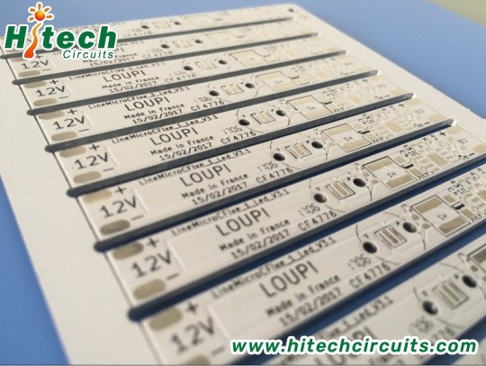

Aluminium PCB
Aluminium PCB are metal-based, copper-clad laminates with a good heat dissipation function. Usually, Aluminium PCB is refer to LED PCB board, which is the most important part of LED display and lighting products, etc.
Hitech Circuits Co., Limited is a professional aluminum pcb board, LED PCB manufacturer in China. Through 10 years of aluminum pcb board designing and manufacturing experience, Hitech are able to provide high quality and cost effective single layer, double layer and multi layer aluminum pcb boards to global customers. For any of your requirements regarding aluminum pcb board, please don’t hesitate to contact [email protected]
#Aluminium PCB#aluminum pcb#pcb assembly#pcb#engineering#technology#pcba#pcb manufacturer#pcbassembly#pcb design#hardware
5 notes
·
View notes
Text
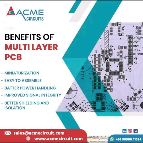
Multilayer PCBs (Printed Circuit Boards) offer numerous advantages over their single-layer or double-layer counterparts. These benefits arise from their enhanced design capabilities, improved performance, and greater flexibility. Here are some key advantages of multilayer PCBs:
#PCB#printed circuit board manufacturers#electronic cable assembly#pcb manufacturing#pcb assembly manufacturer#pcb assembly services#pcb board manufacturer#printed circuit board manufacturer in india#circuit board manufacturing#pcb exporters#pcba#pcb manufacturer#pcb design#pcbassembly#multilayer pcb
2 notes
·
View notes
Text
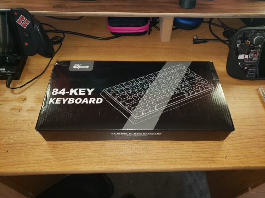
another new toy

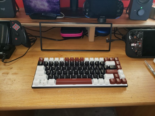

I've been planning to get a number of accessories for my new computer. A new monitor, microphone, maybe one of those vr headsets. But after having it for a few weeks, one thing jumped out as needing an upgrade more urgently than anything else - the stock full size keyboard that came with it was just too large and awkward for my little keyboard shelf. I was tempted to go back to the Microsoft Compact Bluetooth keyboard that I was using with the Steam Deck... but I haven't had a "real" computer, like a proper desktop computer in decades, I wanted a "real" keyboard to go with it. Like a proper mechanical keyboard with switches and buttons and such. And so I typed "mechanical keyboard reviews" into a youtube search, blissfully unaware of the rabbit hole I was about to fall down.
If you know then you already know, but it came as a surprise to me that membrane keyboards are so cheap and so easy to mass produce that they've taken over the casual market altogether, forcing mechanical keyboards into the domain of the ⋆ ˚。⋆˚enthusiast⋆ ˚。⋆˚
Yes, it seems proper keyboards are a hobby now, not a very cheap one either, and the very last thing I need is another expensive hobby. But every hobby has its more affordable and approachable on ramps, and there are a number of pre-built budget boards occupying this space in world of mechanical keyboards. After watching a few dozen hours of youtube videos and reading a bunch of reviews and tutorials, I eventually settled on the RK84 'limited edition' from Royal Kludge for us$80. Which is like twice what I expected to pay when I in my naive innocence began shopping for keyboards, but I've come to understand that eighty bucks absolutely counts as "budget" in this hobby.
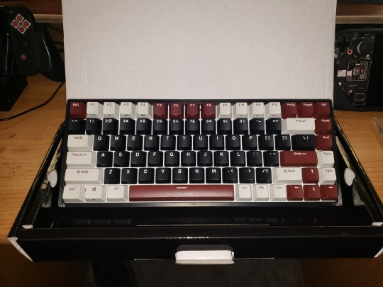
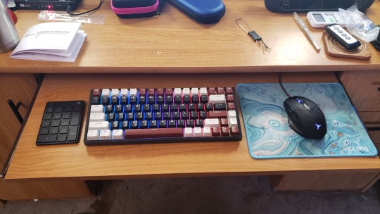
Pricing aside, I really do love my new keyboard. The 75% form factor is ideal, better centering the typing keys and saving a bunch of extra space on my little shelf while maintaining all the functionality of a full size board save only for the number pad. While I do like to use a number pad, I don't mind taking one out when I need it, and the keyboard even has a couple usb ports to easily plug a mouse and separate number pad into, which is super convenient and such an obvious idea that I really have to wonder why all keyboards aren't doubling as USB multi-dongles at this point, with additional usb ports, sd card ports, and so on.
For $10 more than the regular RK84 wireless, the 'limited edition' version has better keycaps, factory-lubed switches, some filler foam in the housing to reduce the hollow sound, an additional layer of sound dampening foam sandwiched between the top plate and the pcb, and a snazzy color scheme, the version I chose combining a black body and mostly black keys with a white top plate that better reflects the swirly rainbow rgb backlighting. The sound is decent, at least to my untrained ear, right out of the box. Which is ideal, as I'd like to avoid the temptation to start modding it.
Because I've gone about as far down this particular rabbit hole as I want to go.
Though I suppose it is tempting to open it up, as some basic tape & band aid mods would be cheap and easy and might improve the sound a bit...
And as much as the pre-lubed yellow linear switches are nice, I did make sure to get a hot-swappable board so it's easy to change them out later if I want to try alternatives, and I do think I might prefer tactile switches for typing...
And the rgb lighting is nice enough that it really is a shame these caps aren't shine though. Yeah, yeah, shine-through is tacky, but Cringe is Dead, and some black top pudding caps might really make the lighting pop. Or maybe a mix of black, white and some accent color to match the color layout that the board came with?
The abyss, it tempts me so...
#mechanical keyboard#keyboards#computers#I really can't be starting any expensive new hobbies#student loan payments start back up in September
3 notes
·
View notes
Text
Price: [price_with_discount] (as of [price_update_date] - Details) [ad_1] Upgrade your cooling experience with Panasonic's latest Air Conditioners, designed to blend technology and performance. As India's 1st Matter enabled RAC, it ensures seamless compatibility with your smart home devices. Powered by MirAie, Panasonic’s intuitive smart home platform, you can control your AC effortlessly via your smartphone or voice assistants. Built for extreme conditions, it provides consistent cooling even at 55°C. The innovative converti7 feature allows you to customize across 7 stages of cooling performance, ensuring optimal comfort and energy efficiency. True AI mode helps to maintain comfort conditioning & saves energy using "Adaptive Thermal Comfort Model". Shield Blu+ technology adds an anti-corrosive coating to both indoor and outdoor unit coils, preventing leakage and doubling the life of heat exchangers. The Eco-Tough casing from Japanese steel safeguards the outdoor unit from tough weather condition. Split AC with inverter compressor: Variable speed compressor which adjusts cooling capacity depending on heat load. The convertible feature with 7 different cooling modes adjusts cooling performances ranging from 45%* to HC*. Therby enhances energy efficiency and provides personalized comfort with minimal effort. Capacity (2.2 Ton): Suitable for large sized rooms (210-250 sq ft); Airflow of 851 CFM; Cooling Capacity of 7850 W & Ambient operating Temperature: upto 55 degree Celsius with 4 way Swing. Energy Rating: 4 Star. Annual Energy Consumption: 1351.04 kWh. ISEER Value: 4.50 . Manufacturer Warranty: 1 year on product, 5 years on PCB, 5 years on ODU Casing and 10 years on compressor. Copper Condenser Coil: Better cooling and requires low maintenance. Healthy Cooling: Equipped with the PM 0.1 Filter to provide clean air by filtering PM 0.1 particles in the air and 3-layered Ag Clean+ Filter provides healthy air. Longer Heat Exchanger Life: Special ShieldBlu+ protection coating to prevent leakages. Key Features- Stabilizer free operation with 145-285 V operating voltage range; Hidden Temperature Display; Noise Level: IDU - 44/50 (db) & ODU: 60 (db). Special Feature: Premium Wi-Fi Inverter Smart Split AC, India's 1st Matter enabled RAC powered by MirAie with 100% Copper Tubing helps in better heat exchange. True AI mode helps to maintain comfort conditioning & saves energy using "Adaptive Thermal Comfort Model". Crystal Clean technology helps in enhancing the cooling performance, provides pure air and saves on electricity bills by self-cleaning of evaporator coils. Refrigerant Gas: R32 – Environment Friendly - "Zero" Ozone Depletion Potential (ODP) Item Dimensions & Net (Gross) Weight: IDU - 110 cm X 25 cm X 33 cm (L x B x H), Outdoor: 87.5 cm X 32 cm X 75 cm (L x B x H), IDU: 15(17.5) Kg, Outdoor: 43.5(51) Kg Included in the box:1 Indoor Unit, 1 Outdoor Unit, Remote Controller, Remote Controller Holder, 2 AAA Battery, User Manual with Warranty Card, Copper Tube (Length: 3.0m) wrapped with Poly-E-Foam, Power Supply Cord (Indoor to Outdoor Connection) [ad_2]
0 notes
Text
Consumer Electronics Printed Circuit Board Market: Key Growth Drivers in the Global Industry

MARKET INSIGHTS
The global Consumer Electronics Printed Circuit Board Market size was valued at US$ 15.34 billion in 2024 and is projected to reach US$ 24.78 billion by 2032, at a CAGR of 6.9% during the forecast period 2025-2032.
Consumer electronic PCBA (Printed Circuit Board Assembly) boards are integrated circuits used across consumer electronics products to mechanically support and electrically connect components through conductive copper pathways. These boards serve as the backbone of modern electronics, encompassing various types including single-layer, double-layer, and multilayer configurations to accommodate different device complexities.
The market growth is primarily driven by accelerating demand for smart devices, including smartphones, wearables, and IoT-enabled home appliances. While China dominates PCB production with over 50% global market share, emerging 5G infrastructure and AI applications are creating new opportunities across multilayer PCBA segments. Furthermore, leading manufacturers like Jabil and Flex Ltd continue expanding production capacities to meet the growing demand for compact, high-performance electronic assemblies.
MARKET DRIVERS
Proliferation of Smart Devices to Fuel Demand for PCBA Boards
The global consumer electronics market continues to expand at an unprecedented rate, with smart devices driving significant demand for high-quality PCBA boards. Smartphones alone accounted for over 1.4 billion units shipped globally in 2023, each requiring sophisticated multilayer PCBA assemblies. The Internet of Things (IoT) revolution has further accelerated this trend, with projections indicating 30 billion connected devices by 2025. These consumer electronics require increasingly complex PCBA solutions that can handle higher processing speeds while maintaining energy efficiency and compact form factors.
Advancements in 5G Technology Accelerating Market Growth
The global rollout of 5G networks represents a pivotal driver for the PCBA board market, as next-generation devices require completely redesigned circuit architectures. 5G-compatible PCBA boards must accommodate higher frequency ranges (up to 52.6 GHz for mmWave implementations) while minimizing signal loss and electromagnetic interference. Carrier aggregation technologies in modern 5G modems often require up to 40% more complex PCBA designs compared to 4G LTE solutions. This technological shift is prompting manufacturers to invest heavily in advanced production capabilities, particularly for high-frequency laminate materials and precision assembly techniques.
Automotive Electronics Evolution Creating New Demand Streams
The automotive sector’s rapid electrification and digital transformation is generating substantial opportunities for PCBA manufacturers. Modern vehicles now incorporate over 100 electronic control units (ECUs) on average, each containing specialized PCBA solutions. The autonomous vehicle segment particularly demands high-reliability boards capable of withstanding harsh environments while processing massive sensor data streams. Premium electric vehicles may contain PCBA components valued at 3-4 times that of conventional automobiles, creating a high-value growth channel for manufacturers with automotive-grade capabilities.
MARKET RESTRAINTS
Supply Chain Vulnerabilities Constraining Market Expansion
The PCBA industry faces significant challenges from global supply chain disruptions, particularly for critical raw materials. Copper prices have shown 35% volatility year-over-year, directly impacting board production costs. Specialty laminate materials and semiconductor components have experienced lead time extensions up to 52 weeks in some cases, creating production bottlenecks. Geopolitical tensions in key manufacturing regions further exacerbate these challenges, forcing companies to maintain larger inventory buffers that negatively impact working capital efficiency.
Environmental Regulations Increasing Compliance Costs
Stringent environmental regulations, particularly concerning lead-free soldering processes and halogen-free laminates, have significantly increased manufacturing complexity. The Restriction of Hazardous Substances (RoHS) directive and similar regulations worldwide now require extensive documentation and testing protocols for each product iteration. Compliance costs for a medium-sized PCBA manufacturer can exceed $500,000 annually, creating substantial barriers to market entry for smaller players. These regulations also necessitate continuous R&D investments to develop alternative materials that meet both performance and environmental requirements.
MARKET CHALLENGES
Miniaturization Demands Outpacing Manufacturing Capabilities
The relentless drive toward smaller, more powerful consumer electronics presents fundamental manufacturing challenges. PCBAs for wearable devices now routinely require trace widths below 50μm and micro-vias under 100μm in diameter, pushing the limits of conventional fabrication techniques. Yield rates for such high-density interconnect (HDI) boards can be 15-20% lower than standard designs, significantly increasing unit costs. This miniaturization trend also demands substantial capital investments in equipment capable of sub-micron precision, with advanced pick-and-place machines often exceeding $500,000 per unit.
Talent Shortage Impacting Technological Advancement
The industry faces a critical shortage of skilled engineers capable of designing and manufacturing next-generation PCBA solutions. Complex RF designs and high-speed digital layouts require specialized expertise that typically takes 5-7 years to develop. The global electronics manufacturing sector currently experiences a 22% vacancy rate for mid-career PCB design engineers, slowing innovation cycles. This skills gap is particularly acute in emerging manufacturing hubs, where educational infrastructure hasn’t kept pace with industry requirements.
MARKET OPPORTUNITIES
AI-Enabled Manufacturing Creating Efficiency Breakthroughs
Artificial intelligence applications in PCBA manufacturing are unlocking unprecedented quality and efficiency improvements. Machine vision systems can now detect assembly defects with 99.98% accuracy, compared to 92% for human inspectors. Predictive maintenance algorithms reduce equipment downtime by 40% in advanced facilities, while AI-optimized panel utilization can decrease material waste by up to 15%. Early adopters of these technologies are gaining significant competitive advantages in both quality consistency and production cost structures.
Emerging Markets Driving Volume Growth
Developing economies represent the next frontier for consumer electronics adoption, creating substantial opportunities for PCBA manufacturers. Smartphone penetration in Southeast Asia and Africa is projected to grow at 8% CAGR through 2030, significantly outpacing mature markets. Local governments are implementing favorable policies to attract electronics manufacturing, including Vietnam’s 10-year tax holidays for high-tech investments. These regions also benefit from younger, tech-savvy populations driving demand for affordable smart devices, creating ideal conditions for volume-focused manufacturing strategies.
CONSUMER ELECTRONIC PCBA BOARD MARKET TRENDS
5G Technology Adoption and High-Density PCBA Demand
The rapid rollout of 5G networks globally is driving significant changes in the consumer electronic PCBA (Printed Circuit Board Assembly) market. As 5G-capable devices require higher frequency and bandwidth performance, manufacturers are shifting toward high-density interconnect (HDI) PCBA boards with advanced materials like low-loss laminates. The global 5G smartphone market is expected to reach over 1.2 billion units by 2025, directly influencing PCBA design requirements. Furthermore, the miniaturization trend in consumer electronics continues to push innovation in multilayer and flexible PCBA solutions, with some manufacturers now offering boards with up to 20+ layers for premium devices.
Other Trends
Automation in PCBA Manufacturing
Consumer electronics manufacturers are increasingly adopting automated surface-mount technology (SMT) lines to improve production efficiency and quality control. This shift is particularly evident in high-volume segments like smartphones and wearables, where precision and consistency are critical. Automated optical inspection (AOI) systems are now being integrated into production lines at a rate exceeding 30% annually, reducing defects by up to 60% compared to manual inspection. As labor costs rise in traditional manufacturing hubs, this automation trend is becoming crucial for maintaining competitiveness.
Sustainability Initiatives Reshaping Materials and Processes
Environmental regulations and consumer preferences are driving significant changes in PCBA materials and manufacturing processes. The European Union’s Restriction of Hazardous Substances (RoHS) directive and similar regulations worldwide have accelerated the adoption of lead-free soldering and halogen-free laminates. Recent market data shows that over 85% of new PCBA production now complies with RoHS standards, up from just 60% five years ago. Additionally, manufacturers are investing in closed-loop recycling systems for precious metals recovered from PCBA waste, with some achieving recovery rates exceeding 90% for gold and silver.
COMPETITIVE LANDSCAPE
Key Industry Players
Market Leaders Invest in Advanced Manufacturing and Strategic Partnerships
The global Consumer Electronic PCBA Board market features a fragmented yet highly competitive landscape dominated by established manufacturers and emerging regional players. Among these, Jabil and Flex Ltd maintain leading positions, owing to their extensive production capabilities and engagements with multinational electronics brands. These Tier-1 manufacturers collectively held approximately 18% of the global market share in 2024, supported by vertically integrated supply chains and investments in high-mix, low-volume (HMLV) manufacturing.
Meanwhile, Chinese firms like Shennan Circuits Company Limited (SCC) and Avary Holding have expanded aggressively, leveraging cost efficiencies and government-backed semiconductor policies. SCC reported consecutive revenue growth above 12% YoY, capitalizing on domestic smartphone manufacturers’ demand for multilayer PCBAs. The company’s recent acquisition of a German PCB fabricator signifies its ambitions in the European automotive electronics segment.
While major players focus on capacity expansions, mid-sized competitors such as Victory Giant Technology (VGT) differentiate through certified quick-turn prototyping services essential for IoT device makers. Notably, VGT partnered with Xiaomi and Oppo to develop high-frequency PCBA solutions for 5G smartphones, demonstrating innovation-driven competition.
Meanwhile, supply chain disruptions prompted firms like Palpilot International to localize production – establishing plants in Mexico and Vietnam to bypass tariff risks. Such strategic realignments reflect the industry’s shift toward regionalization while sustaining just-in-time delivery models.
List of Key Consumer Electronic PCBA Board Companies Profiled
Jabil Inc. (U.S.)
Flex Ltd. (Singapore)
Shenzhen Fastprint Circuit Tech (China)
Kingbrother Electronics (China)
Shennan Circuits Co. Ltd (China)
Avary Holding (Shenzhen) Co. Ltd. (China)
Victory Giant Technology (China)
Aoshikang Technology (China)
Camelot Electronics Technology (China)
Lensuo Technology Development (China)
Segment Analysis:
By Type
Multilayer PCBA Board Segment Dominates Due to Increasing Demand for High-Density Electronics
The market is segmented based on type into:
Single-layer PCBA Board
Double-layer PCBA Board
Multilayer PCBA Board
By Application
Smartphone Segment Holds Maximum Share Owing to Rising Global Smartphone Adoption
The market is segmented based on application into:
Smart Phone
Tablet
Smart Wear
TV Set
Air Conditioner
Others
By Technology
Surface Mount Technology Leads Due to Higher Efficiency and Compact Design Capabilities
The market is segmented based on technology into:
Through-hole Technology
Surface Mount Technology
Mixed Technology
By Material
FR4 Substrate Maintains Dominance as Industry Standard for Consumer Electronics
The market is segmented based on material into:
FR4 Substrate
Flexible Substrate
High-frequency Substrate
Others
Regional Analysis: Consumer Electronic PCBA Board Market
North America The North American PCBA Board market is characterized by high-value, technology-driven demand, particularly for advanced multilayer boards used in premium consumer electronics. The United States accounts for over 85% of regional demand, fueled by strong R&D investment and the presence of tech giants like Apple and Google. While the market faces cost pressures due to labor and material expenses, manufacturers are increasingly adopting automation to maintain competitiveness. Environmental regulations such as RoHS compliance influence material selection, pushing suppliers toward lead-free and halogen-free solutions. Canada’s market is smaller but growing steadily, supported by telecommunications equipment demand.
Europe European PCBA manufacturers focus on high-quality, precision-engineered boards for automotive, industrial, and consumer applications. Germany leads in production capabilities, housing several global EMS providers. The EU’s circular economy action plan drives innovation in recyclable PCB materials and processes. Though labor costs remain high compared to Asia, European manufacturers differentiate through advanced manufacturing techniques and stringent quality control. The UK and France show particular strength in aerospace and defense applications that require specialized PCBA solutions. Brexit-related supply chain disruptions have prompted some reshoring of PCB production within the EU.
Asia-Pacific As the global manufacturing hub for PCBA boards, Asia-Pacific dominates with over 70% of worldwide production capacity. China’s massive electronics ecosystem drives demand for cost-efficient, high-volume PCBs, with Shenzhen serving as a key production cluster. Japanese and Korean manufacturers lead in advanced HDI and flex PCB technologies for premium devices. Rapid urbanization across Southeast Asia is creating new consumer electronics markets, though infrastructure gaps sometimes hinder supply chain efficiency. The region benefits from vertical integration, with many PCB fabricators also offering assembly services. Intense competition keeps margins thin but fosters continuous process optimization.
South America South America’s PCBA market remains modest but developing, primarily serving domestic consumer electronics manufacturers. Brazil accounts for nearly half of regional demand, though economic instability often delays capital investments in PCB manufacturing. Most complex boards are imported from Asia, while local facilities focus on simpler designs. Currency fluctuations impact material procurement costs, causing pricing volatility. Some countries like Argentina are implementing import substitution policies to boost local PCB production, though technological limitations constrain capabilities. The growing middle class is driving demand for affordable smartphones and appliances, creating opportunities for PCB suppliers.
Middle East & Africa This emerging market shows potential as electronics manufacturing gradually expands beyond oil-dependent economies. Israel stands out for its high-tech PCB applications in defense and telecommunications. UAE and Saudi Arabia are investing in technology parks to attract electronics manufacturers, though most PCBs are still imported. Limited local expertise in complex board design and manufacturing hampers development, leading to reliance on foreign partners. South Africa serves as a regional hub, with some capability for basic PCB production. Infrastructure challenges and fragmented supply chains remain barriers, though government initiatives aim to develop local electronics manufacturing ecosystems.
Report Scope
This market research report provides a comprehensive analysis of the global and regional Consumer Electronic PCBA Board markets, covering the forecast period 2025–2032. It offers detailed insights into market dynamics, technological advancements, competitive landscape, and key trends shaping the industry.
Key focus areas of the report include:
Market Size & Forecast: Historical data and future projections for revenue, unit shipments, and market value across major regions and segments. The global market was valued at USD 12.8 billion in 2024 and is projected to reach USD 18.3 billion by 2032, growing at a CAGR of 4.6%.
Segmentation Analysis: Detailed breakdown by product type (single-layer, double-layer, multilayer), application (smartphones, tablets, wearables, home appliances), and end-user industry to identify high-growth segments.
Regional Outlook: Insights into market performance across North America, Europe, Asia-Pacific, Latin America, and Middle East & Africa. Asia-Pacific dominates with 68% market share in 2024, led by China’s manufacturing ecosystem.
Competitive Landscape: Profiles of 15 leading manufacturers including Jabil, Flex Ltd, Shenzhen Fastprint, and Shennan Circuits, analyzing their market share (top 5 companies hold 32% share), capacity expansions, and technological partnerships.
Technology Trends: Assessment of HDI boards, flexible PCBs, embedded components, and IoT integration driving innovation. The multilayer PCB segment accounts for 54% revenue share in 2024.
Market Drivers & Restraints: Evaluation of 5G adoption, smart device proliferation, and supply chain localization benefits versus raw material price volatility and geopolitical trade tensions.
Stakeholder Analysis: Strategic insights for PCB fabricators, EMS providers, OEMs, and investors regarding capacity planning, technology roadmaps, and emerging applications like AR/VR devices.
Related Reports:https://semiconductorblogs21.blogspot.com/2025/06/global-video-sync-separator-market.htmlhttps://semiconductorblogs21.blogspot.com/2025/06/silicon-rings-and-silicon-electrodes_17.htmlhttps://semiconductorblogs21.blogspot.com/2025/06/ceramic-bonding-tool-market-investments.htmlhttps://semiconductorblogs21.blogspot.com/2025/06/coaxial-panels-market-challenges.htmlhttps://semiconductorblogs21.blogspot.com/2025/06/oled-and-led-automotive-light-market.htmlhttps://semiconductorblogs21.blogspot.com/2025/06/gas-cell-market-demand-for-ai-chips-in.htmlhttps://semiconductorblogs21.blogspot.com/2025/06/digital-demodulator-ic-market-packaging.htmlhttps://semiconductorblogs21.blogspot.com/2025/06/nano-micro-connector-market.htmlhttps://semiconductorblogs21.blogspot.com/2025/06/single-mode-laser-diode-market-growth.htmlhttps://semiconductorblogs21.blogspot.com/2025/06/silicon-rings-and-silicon-electrodes.htmlhttps://semiconductorblogs21.blogspot.com/2025/06/battery-management-system-chip-market.htmlhttps://semiconductorblogs21.blogspot.com/2025/06/scanning-slit-beam-profiler-market.htmlhttps://semiconductorblogs21.blogspot.com/2025/06/atomic-oscillator-market-electronics.htmlhttps://semiconductorblogs21.blogspot.com/2025/06/plastic-encapsulated-thermistor-market.htmlhttps://semiconductorblogs21.blogspot.com/2025/06/ceramic-bonding-tool-market-policy.html
0 notes
Text
PCB Fabrication Company in India – Your Partner in Quality Electronics Manufacturing
Printed Circuit Boards (PCBs) are the foundation of every electronic device we use today. From smartphones to electric vehicles, PCB fabrication plays a critical role in bringing ideas to life. India has emerged as a preferred destination for PCB fabrication services, offering a perfect mix of technology, talent, and cost-effectiveness.
If you are looking for the right PCB fabrication company in India, this guide will help you understand the benefits of working with Indian manufacturers and how FindingMFG simplifies the process of finding trusted partners.
Why India for PCB Fabrication?
India’s electronics sector is expanding rapidly, and PCB manufacturing is at the heart of this growth. Here’s why global businesses choose India for their PCB needs:
1️⃣ Competitive Pricing with Global Standards
Indian PCB fabrication companies deliver high-quality boards at competitive rates. Whether you need simple single-layer PCBs or advanced multilayer designs, Indian manufacturers combine affordability with world-class production standards.
2️⃣ Advanced Manufacturing Capabilities
Top Indian PCB manufacturers use cutting-edge machinery and follow international quality certifications such as ISO, RoHS, and IPC standards. This ensures precision, durability, and reliability in every product.
3️⃣ Government Support and Incentives
Initiatives like Make in India and the PLI scheme are designed to strengthen India’s position in the global electronics manufacturing ecosystem, helping PCB companies invest in new technologies and infrastructure.
4️⃣ Skilled Engineering Talent
India’s large pool of skilled engineers and technicians gives it a major edge in delivering both prototype PCBs and high-volume production.
Key Services Offered by PCB Fabrication Companies in India
Indian PCB manufacturers provide comprehensive services to meet diverse customer needs:
Single, Double & Multilayer PCB Production
Rigid, Flexible, and Rigid-Flex PCBs
High-Frequency and HDI (High-Density Interconnect) PCBs
Prototype Development with Fast Turnaround
PCB Assembly and Testing
Whether you need boards for prototypes or mass production, India’s manufacturers can deliver with efficiency and precision.
Industries That Rely on Indian PCB Manufacturers
Indian PCB fabrication companies supply essential components to industries such as:
Consumer Electronics
Automotive and Electric Vehicles (EV)
Telecommunications
Healthcare and Medical Devices
Aerospace and Defense
Industrial Equipment
Their ability to meet strict quality and performance standards makes them trusted partners for both domestic and international markets.
Finding the Right PCB Fabrication Company with FindingMFG
Choosing the right PCB fabrication company in India can be challenging if you don’t know where to look. That’s where FindingMFG makes the difference.
FindingMFG connects you with a wide network of verified PCB manufacturers in India, helping you find partners who align with your project requirements.
✅ Verified and Trusted Suppliers
Every supplier listed on FindingMFG is verified for authenticity, capability, and delivery performance.
✅ Easy Requirement Posting
You can post your manufacturing requirements directly on the platform, receive multiple quotes, and select the best fit for your project.
✅ Global Reach with Local Expertise
Whether you’re sourcing PCBs for local projects or global exports, FindingMFG helps you find the right supplier for your needs.
Conclusion
India’s PCB fabrication industry is growing rapidly, driven by advanced technology, skilled expertise, and government support. By choosing a PCB fabrication company in India, you’re ensuring quality, affordability, and innovation for your electronic products.
Ready to connect with the best manufacturers? 👉 Visit www.findingmfg.com and start your journey today.
FindingMFG — Your Trusted Platform for Global Manufacturing Solutions
0 notes
Text
Smart Mobility Drives Smart PCBs: Market to Hit $4.4Bn by 2035
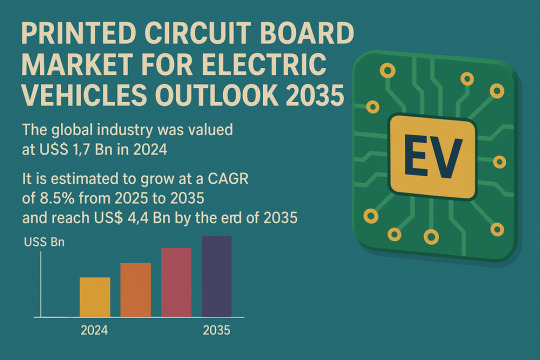
The global Printed Circuit Board (PCB) Market for Electric Vehicles (EVs) is set to witness significant expansion over the next decade, according to the latest market analysis. Valued at US$ 1.7 billion in 2024, the market is projected to grow at a CAGR of 8.5% from 2025 to 2035, reaching a valuation of US$ 4.4 billion by the end of the forecast period.
Market Overview: Printed Circuit Boards (PCBs) are the electronic backbone of electric vehicles, enabling power distribution, connectivity, and control across critical systems such as battery management, motor control, infotainment, and advanced safety features. With EV adoption accelerating globally, PCBs have become essential to the performance, reliability, and innovation of next-generation vehicles.
Market Drivers & Trends
One of the primary drivers of this market is the growing investment and strategic partnerships in the EV supply chain. Leading automakers and electronics companies are heavily investing in R&D and manufacturing capacity to meet the increasing demand for high-performance PCBs.
Moreover, the rise of autonomous and connected vehicles has made sophisticated electronics an indispensable part of modern transportation. The proliferation of features like ADAS (Advanced Driver-Assistance Systems), V2X communication, and in-vehicle infotainment is pushing the demand for compact, multi-layer, high-speed, and thermally efficient PCBs.
In 2023, EV sales in the U.S. surged by 60%, while the European Commission invested over US$ 6 billion in EV infrastructure further stimulating demand for advanced PCB solutions.
Latest Market Trends
The industry is witnessing a rapid shift toward flexible and high-density interconnect (HDI) PCBs, which are crucial for compact and space-saving vehicle designs. Flexible PCBs, in particular, are gaining traction in battery management systems and advanced sensor modules due to their lightweight and adaptable nature.
Additionally, regulatory advancements such as the FCC's allocation of the 5.9 GHz band for vehicle safety and autonomous functions have opened doors for new PCB capabilities. Real-time, high-speed data transmission requires advanced PCB materials and multi-layer configurations.
Key Players and Industry Leaders
Some of the most prominent players shaping the global printed circuit board market for electric vehicles include:
ABL CIRCUITS
AT&S Austria Technologie & Systemtechnik Aktiengesellschaft I
Chin Poon Industrial Co., Ltd.
Compeq Manufacturing Co., Ltd.
HannStar Board Corporation
Kinwong Electronic Co. Ltd
LG Innotek
MEIKO ELECTRONICS Co., Ltd.
Nan Ya Printed Circuit Board Corporation
RayMing PCB
Rush PCB Ltd.
SCHWEIZER ELECTRONIC AG
Shenzhen Capel Technology Co., Ltd.
Shenzhen Fastprint Circuit Tech Co., Ltd.
TTM Technologies
Unimicron Technology Corporation
Victory Giant Technology Co., Ltd.
WUS Printed Circuit Co., Ltd.
Young Poong Group
Zhen Ding Tech. Group
Among Others
These companies are prioritizing innovation, expanding global manufacturing footprints, and forging strategic alliances to maintain competitiveness and cater to evolving industry needs.
Download now to explore primary insights from our Report in this sample - https://www.transparencymarketresearch.com/sample/sample.php?flag=S&rep_id=86464
Recent Developments
October 2024 – Mektech Manufacturing announced a 920 million baht investment in Thailand to expand production capacity for flexible PCBs and FPCBA used in electric vehicles.
July 2024 – Omron Electronic Components Europe launched a high-power PCB relay for Level 2 EV charging stations. The innovation features double-break contact designs, enabling reduced heat dissipation and enhanced energy efficiency.
Market Opportunities
The market is poised for significant opportunities, particularly in:
OEM collaborations to co-develop application-specific PCBs for power electronics and smart mobility.
Flexible PCB technology, which is expected to revolutionize EV design with lightweight, customizable circuit boards.
Geographical expansion into regions like South Asia and Latin America, where EV adoption is accelerating, and supply chains are emerging.
Additionally, the ongoing reshoring of PCB manufacturing in regions such as North America and Europe presents untapped potential for local players.
Future Outlook
According to analysts, the convergence of EV electrification, autonomy, and connectivity will demand ever more sophisticated PCB solutions. Next-generation EVs will require PCBs capable of managing 50 Gbps data speeds, robust thermal management, and high signal integrity. Flexible, multilayer, and ceramic PCBs are expected to gain ground rapidly.
As regulations around emissions and vehicle safety become more stringent, automakers will rely heavily on advanced PCB solutions to remain compliant and competitive. From battery optimization to smart in-vehicle systems, the demand for high-performance PCBs is set to skyrocket.
Market Segmentation
The global PCB market for EVs is segmented across several parameters:
By Type: Multilayer (dominant with 73.98% market share in 2024), Double-sided, Single-sided
By Substrate Type: HDI/Micro-via/Build-up, Flexible, Rigid-flex, Rigid 1-2 Sided
By Material: FR4, Metal-Based, Ceramic, PTFE, Power Combi-boards
By Application: ADAS, Battery Management, Powertrain, Lighting & Display, Charging, Connectivity, etc.
By Vehicle Type: Passenger Cars, Buses, Two-Wheelers, Trucks, Off-Highway Vehicles
By End Users: OEMs, Tier 1 & 2 Suppliers, Aftermarket
Regional Insights
East Asia is the undisputed leader in the global market, accounting for 68.3% of the total share in 2024. The region’s dominance stems from:
A well-established electronics manufacturing ecosystem
Government support for EV expansion and green technology
Cost-effective production and high R&D capabilities
Japan, South Korea, and China house the majority of leading PCB suppliers and EV component manufacturers. Their early investment in automation and material innovation is positioning East Asia as the global hub for EV electronics.
Other key regions include:
North America, driven by government initiatives like the CHIPS Act
Europe, focused on sustainable manufacturing and reducing supply chain reliance on Asia
South Asia, emerging as a low-cost, high-volume manufacturing zone
Why Buy This Report?
This in-depth industry report offers:
Detailed market sizing and forecast (2020–2035)
Comprehensive segmentation across product, material, vehicle type, and region
Competitive landscape with profiles of 20+ leading companies
Insights into trends, innovations, and regional dynamics
Strategic recommendations for stakeholders, investors, and policymakers
Whether you're an investor, OEM, component supplier, or policy planner, this report serves as a strategic guide to understanding growth dynamics and identifying emerging opportunities in the PCB market for electric vehicles.
Explore Latest Research Reports by Transparency Market Research: Active Optical Cable Market: https://www.transparencymarketresearch.com/active-optical-cables.html
3D Cameras Market: https://www.transparencymarketresearch.com/3d-cameras-market.html
Optoelectronics Market: https://www.transparencymarketresearch.com/optoelectronics-market.html
Machine Safety Market: https://www.transparencymarketresearch.com/machine-safety-market.html
DC-DC Converter OBC Market: https://www.transparencymarketresearch.com/dc-dc-converter-obc-market.html
About Transparency Market Research Transparency Market Research, a global market research company registered at Wilmington, Delaware, United States, provides custom research and consulting services. Our exclusive blend of quantitative forecasting and trends analysis provides forward-looking insights for thousands of decision makers. Our experienced team of Analysts, Researchers, and Consultants use proprietary data sources and various tools & techniques to gather and analyses information. Our data repository is continuously updated and revised by a team of research experts, so that it always reflects the latest trends and information. With a broad research and analysis capability, Transparency Market Research employs rigorous primary and secondary research techniques in developing distinctive data sets and research material for business reports. Contact: Transparency Market Research Inc. CORPORATE HEADQUARTER DOWNTOWN, 1000 N. West Street, Suite 1200, Wilmington, Delaware 19801 USA Tel: +1-518-618-1030 USA - Canada Toll Free: 866-552-3453 Website: https://www.transparencymarketresearch.com Email: [email protected]
0 notes
Text
Victory – Delivering High-Precision PCBs for Today’s Electronics Industry
Victory, established in 2005, has earned a strong reputation as a professional PCB manufacturer known for delivering top-tier printed circuit boards tailored for today’s dynamic and demanding electronics landscape. With nearly two decades of industry experience, Victory specializes in producing a wide variety of PCB types, offering flexibility in small to medium-sized production runs and quick-turn manufacturing to support customers’ time-sensitive needs.
Victory’s manufacturing model is built on the foundation of the “3H” principle—high quality, high precision, and high density. These three pillars ensure that every PCB manufactured meets strict international standards and functions reliably in real-world applications, whether in consumer electronics, industrial control systems, telecommunications, or medical devices.
Operating out of a state-of-the-art 30,000-square-meter production facility in Shenzhen, Victory has the capacity to produce 60,000 square meters of PCBs and up to 3,000 different parts each month. This significant capacity, coupled with advanced production and testing equipment, enables Victory to handle both complex custom designs and high-volume orders with ease.
What sets Victory apart is its robust in-house quality system that governs every phase of production—from material sourcing and engineering to final testing and delivery. Each PCB undergoes rigorous checks to ensure dimensional accuracy, electrical integrity, and durability. This meticulous attention to detail results in boards that perform flawlessly even under the most challenging operational environments. Click here victorypcb.com
In addition to its focus on manufacturing excellence, Victory is known for its responsiveness and customer-centric approach. The company works closely with clients to provide technical guidance, assist with design optimization, and offer tailored production solutions. This collaborative spirit has helped Victory build lasting relationships with customers worldwide.
Speed is another hallmark of Victory’s service. The company’s quick-turn capabilities allow for rapid prototyping and fast delivery, helping businesses reduce development cycles and accelerate product launches. This is especially valuable for startups and innovators bringing new technologies to market.
Victory’s comprehensive capabilities, advanced infrastructure, and dedication to quality make it a standout in the competitive world of PCB manufacturing. Whether you need standard double-layer PCBs, multi-layer boards, or high-density interconnect solutions, Victory provides the reliability and performance your products demand.
1 note
·
View note
Text
Structural Innovation and Easy Installation Technologies in Power Socket Design

As smart homes, office automation, and industrial digitalization rapidly advance, the demand for user-friendly, efficient, and safe power sockets continues to grow. Traditional socket designs are no longer sufficient for fast-paced environments that require high reliability, ease of installation, and space optimization. This has driven innovation in both internal structure and external mounting mechanisms of modern power sockets.
This article explores key advancements in structural design and installation technologies of power sockets, focusing on terminal innovations, mounting bracket designs, and strategies to increase module density without increasing volume. We will also discuss real-world examples and applicable technologies for B2B manufacturers and system integrators.
1. Integrated vs. Modular Terminal Design: Which is More Efficient?
The terminal structure of a power socket directly determines wiring efficiency and stability. The two mainstream types are:
A. Integrated Terminal Block (One-Piece)
All terminals are integrated into a single housing.
Benefits: Shorter installation time. Reduced loose contacts. Lower resistance due to shorter conductive paths.
Limitations: Less flexible for modular replacement. May increase overall production complexity.
B. Modular Terminal Block (Multi-Part)
Each terminal is separately assembled or replaceable.
Benefits: Ideal for custom configurations. Easier to repair and replace.
Limitations: Longer assembly time. Risk of performance inconsistency.
2. Push-in Spring Connection Technology: Fast, Safe, Tool-Free Wiring
Compared to screw terminals, push-in spring terminals provide:
Quick installation: Simply push the stripped wire into the terminal.
Strong contact: Stainless steel or beryllium copper springs maintain pressure for years.
No need for torque tools: Reduces operator training and tool investment.
🔧 Case Example: A European power socket brand uses a push-in spring design that allows a full 5-gang module to be wired in under 30 seconds — 60% faster than screw terminals.
3. Quick-Mount Bracket Designs: Screw-Free, Time-Saving, and Reliable
In large-scale installations (e.g., hotels, office buildings), fast mounting systems dramatically reduce labor costs and error rates.
Key Innovations:
A. Snap-In Mounting Frame
Socket modules are inserted directly into wall plates with audible clicks.
Uses elastic clips or sliding locks for firm placement.
Ideal for drywall and modular building systems.
B. Screwless Embedded Mounting
Eliminates screw holes by using slide-in rail structures.
Allows easy front-facing maintenance or upgrades.
Common in premium wall systems and panel furniture.
C. Magnetic or Cam-Lock Fastening
Applies in high-end modular offices.
Enables tool-free repositioning.
🔧 Case Example: A Chinese manufacturer developed a double-locking quick-install bracket that passed 500N pull force tests, suitable for vibration-prone environments like rail stations.
4. Increasing Module Density Without Expanding Volume
Modern installations demand multi-functionality in limited space. Techniques include:
A. Vertical Layering of Internal PCB
Using 3D layout: control, relay, and detection circuits are stacked.
Reduces horizontal footprint while maintaining thermal separation.
B. Multi-Function Integration
Combining USB chargers, smart sensors, and energy monitors in one unit.
Example: A 55x55mm wall socket includes 2 USB-A ports, 1 USB-C PD port, and Wi-Fi controller.
C. High-Density Terminal Design
Dual-row spring contacts with insulation barriers allow up to 10 terminals in standard footprint.
Ensures safety spacing while maintaining compact size.
5. Material Innovation: Making Structural Compactness Possible
A. High-Performance Plastics:
Use of PA66, PC+ABS, and flame-retardant PBT with thin-wall molding tech.
Improves space efficiency without sacrificing insulation performance.
B. Conductive Material Optimization:
Use of laminated copper busbars.
Electroplated or stamped silver contact surfaces to reduce thickness.
6. Installation Aids and Engineering Enhancements
A. Color-coded Wiring Guides:
Reduces wiring errors during bulk installations.
Accelerates compliance with local electrical codes.
B. Pre-assembled Harnesses:
For standard socket layouts, pre-assembled wire bundles reduce on-site labor.
C. Tool-Assisted Plug-In Systems:
Modular rail sockets with plug-in interfaces (e.g., DIN-rail smart outlets) improve interchangeability.
7. Structural Testing and Validation

8. Conclusion: Towards Smarter, Faster, and Denser Power Socket Design
Power socket structure and installation are no longer just mechanical tasks—they are core parts of user experience, energy efficiency, and engineering cost control. Through structural innovation like push-in terminals, quick-install brackets, and functional integration in compact modules, manufacturers can deliver plug-and-play, space-saving, and intelligent power socket solutions.
Whether you're a B2B buyer, an engineering contractor, or a systems integrator, adopting these next-generation socket designs will result in lower maintenance costs, faster deployment, and greater end-user satisfaction.
en.dghongju.com
0 notes
Text

Bergquist Aluminum PCB board manufactured by Hitech
Aluminum PCB board, also named aluminum-based PCB, metal clad (MCPCB) PCB, insulated metal substrate (IMS or IMPCB) PCB, thermally conductive PCBs, etc. Aluminum printed circuit board (PCB) is a unique metal-based copper clad laminate with good thermal conductivity, electrical insulation performance and mechanical processing performance. It is composed of copper foil, thermally conductive insulating layer and metal substrate. It is generally including single layer, double layer and multilayer aluminum PCB board.
Email Cynthia: [email protected] if you are interested in PCB and PCBA service.
0 notes
Text
Learn the Traits to Find the Best Mcpcb Manufacturer for Your Needs
Metal-core printed circuit boards are one of the most significant spare parts you need to operate and control electronic goods. The quality of this spare will affect the functioning of the entire device. Hence, the manufacturers and the suppliers of the product are some of the elemental stakeholders for electronic device-producing brands. Naturally, due to massive demand, you can find several makers and suppliers in the industry. In this article, we will discuss the traits to discern the best.
Years of experience
The first aspect which you must find out to work with the best mcpcb manufacturer is the number of years for which the company has been operational in the market. You must look for a brand which has been in the market for a minimum of one and a half decades.
Service Array
Services from the top manufacturers and suppliers can help patrons get the best value for their investment. Some of the vital services you can get from the market leaders is mcpcb assembly, mass production, product prototype and innovative designing. These brands are masters in customization and they can change and adapt their products as per the precise customer requirements.
Product Array
Apart from service variety these brands can also act as some of the best single window service providers for different products like single layer metal core pcb, double sided metal core pcb, two layer aluminum base pcb and multilayer aluminum base pcb. Hence irrespective of your requirement specifications you can turn to a single vendor to meet all your business needs.
Quality control certificate
Finally, before you select a vendor for your business one of the main things which you must check is quality assurance certifications for the products from the vendor. This is one of the parameters that give you assurance for the product quality into which you are investing and also for their internal procedures and organization culture. These are the vendors who can add much value to your business.
0 notes
Text
Surface Finishes for Multilayer PCBs and Their Impact
Multilayer PCBs are essential in modern electronic systems where high-density routing, signal integrity, and reliability are critical. While inner layers are encapsulated during lamination, the outer layers of a multilayer PCB are exposed for component assembly — making surface finish a key factor in performance and long-term reliability.
Surface finish not only protects the exposed copper but also directly influences soldering quality, component compatibility, and board lifespan, especially in complex multilayer designs.
Why Surface Finish Is Critical in Multilayer PCBs
In a multilayer PCB, especially those with 6, 8, or more layers, outer-layer copper traces and pads are often extremely dense and designed for fine-pitch SMT components such as BGAs, QFNs, or high-pin-count connectors.
A good surface finish must:
Ensure consistent solderability across dense pad arrays
Maintain flatness to support reliable assembly of micro-components
Provide oxidation protection during storage and processing
Be compatible with lead-free reflow profiles
Handle multiple reflow cycles without degradation
Multilayer PCBs often undergo more complex assembly and higher thermal stress, so the surface finish must meet higher standards than simple single- or double-layer boards.
Common Surface Finishes for Multilayer PCBs
1. ENIG (Electroless Nickel Immersion Gold)
The most popular surface finish for multilayer boards, especially in high-density and high-reliability applications.
Provides excellent flatness for fine-pitch components (e.g. BGAs)
Stable during multiple reflow cycles
Compatible with high-speed signals due to smooth surface
Long shelf life, ideal for staged assembly
Slightly higher cost but justified by performance
Widely used in servers, telecom equipment, and aerospace PCBs.
2. OSP (Organic Solderability Preservative)
Preferred for cost-sensitive multilayer boards with fine-pitch components.
Flat surface suitable for automated SMT
Environmentally friendly and lead-free
Lower cost than ENIG
Limited shelf life, requires controlled handling
Not ideal for boards requiring multiple assembly cycles
Often used in consumer electronics and automotive applications.
3. Immersion Silver
Used for multilayer boards requiring high signal integrity or RF performance.
Low surface roughness ensures good impedance control
Suitable for high-frequency multilayer PCBs
Sensitive to tarnishing and handling
Better electrical performance than ENIG in certain designs
Good choice for communication equipment and high-speed digital boards.
4. Lead-Free HASL
Sometimes used in low-cost multilayer boards, but not recommended for very dense designs.
Cost-effective, robust finish
Less flat surface can cause soldering issues on fine-pitch pads
May lead to solder bridging in dense layouts
Acceptable for through-hole or mixed technology boards
Usually applied to industrial control or power-related multilayer PCBs.
Surface Finish Considerations in Multilayer PCB Design
When choosing a surface finish for multilayer PCBs, consider:
Assembly method (SMT vs through-hole, single vs multiple reflows)
Pad density and component type (especially fine-pitch packages)
Signal performance needs (RF, impedance control, etc.)
Environmental factors (RoHS, storage conditions)
Budget vs reliability trade-offs
In many high-reliability or mission-critical multilayer designs, ENIG or Immersion Silver is preferred despite higher cost, due to their consistent performance.
Final Thoughts
The outer layers of a multilayer PCB may seem like a small part of a complex system, but the choice of surface finish can make or break the final product. Whether it's ensuring reliable solder joints for 0.4 mm pitch BGAs, withstanding multiple reflow cycles, or maintaining performance in high-frequency circuits — the right surface finish is critical.
Understanding the relationship between board complexity, material stack-up, and surface treatment is essential for delivering a reliable, high-performance multilayer PCB.

0 notes
Text
Understanding the Pogo Pin Connector: Precision, Performance, and Versatility in Modern Electronics
What is a Pogo Pin Connector?
A pogo pin connector, also known as a spring-loaded contact, is a precision-made electrical component used to establish a reliable connection between two electronic devices. Consisting of a plunger, a barrel, and a spring, the pogo pin ensures consistent pressure and secure contact in a wide range of environments. Its unique design allows it to compress and expand, offering durability and stability even under repeated usage.

Pogo pin connectors are the backbone of modular, test, and high-cycle electronic designs, offering seamless and swift connectivity for both temporary and semi-permanent connections.
Key Components of a Pogo Pin Connector
Understanding the anatomy of a pogo pin is crucial to appreciating its performance capabilities:
Barrel: The outer shell, typically made of brass or phosphor bronze, which houses the internal components.
Plunger: The movable head that makes direct contact with the mating surface.
Spring: A high-precision coil spring that maintains consistent force and enables thousands of mating cycles.
Surface Plating: Gold-plated layers ensure excellent conductivity, corrosion resistance, and minimal electrical loss.
Each component is meticulously engineered to maintain low contact resistance, enhance electrical conductivity, and ensure long operational life.
Advantages of Using Pogo Pin Connectors
The versatility of pogo pins makes them ideal for applications across industries. Here are the standout benefits:
1. High Durability and Longevity
Thanks to robust internal springs and quality plating (typically 10µ” or more of gold), pogo pin connectors are rated for up to 1 million mating cycles.
2. Space-Saving Design
These connectors are compact, making them suitable for miniaturized electronics, wearable devices, and smartphones, where space is at a premium.
3. Superior Electrical Performance
Low and stable contact resistance ensures reliable signal transmission, which is critical in data, RF, and power transfer applications.
4. Easy Maintenance and Replacement
Unlike soldered connections, pogo pins offer non-permanent, quick-swap interfaces, making them ideal for testing environments and prototyping.

Applications of Pogo Pin Connectors
Pogo pin connectors have become a cornerstone in several industries:
1. Consumer Electronics
Used in charging docks, headphones, smartwatches, and smartphones, pogo pins offer quick connect/disconnect functionality.
2. Medical Devices
Precision and reliability make them ideal for diagnostic equipment, wearables, and implantable devices, where minimal electrical loss and hygiene are essential.
3. Automotive Systems
In cars, pogo pins are used in test equipment, electronic control units (ECUs), and diagnostic modules, where vibration resistance is crucial.
4. Industrial Testing
Automated Test Equipment (ATE) depends heavily on pogo pins for circuit board testing, ensuring quick, reliable, and repeatable measurements.
5. Military and Aerospace
In mission-critical systems, pogo pin connectors are preferred for their mechanical resilience, electrical reliability, and compact form factor.
Types of Pogo Pin Connectors
Different designs address specific performance and spatial requirements:
Through-Hole Pogo Pins: Designed for PCB mounting with high mechanical strength.
Solder Cup Pogo Pins: Ideal for hand-soldered wire connections.
Surface Mount Pogo Pins (SMT): Support automated SMT processes, great for mass production.
Double-Ended Pogo Pins: Used in battery packs and modular devices, offering dual connectivity points.
Waterproof Pogo Pins: Encased in sealing materials for applications in harsh or moist environments.
Material and Coating Considerations
The material and coating of pogo pins determine their electrical and mechanical characteristics:
Base Material: Brass and beryllium copper are common, offering a balance of strength and conductivity.
Spring Material: Typically stainless steel or music wire for maximum flexibility and cycle life.
Plating: Gold over nickel is standard for excellent corrosion resistance and electrical stability.
Custom plating options include palladium-nickel or rhodium for specific high-wear or high-frequency applications.
Design Considerations for Pogo Pin Connectors
When integrating pogo pin connectors into a system, several factors need to be considered:
1. Contact Force
Selecting the right spring force is essential to ensure stable connections without damaging mating surfaces.
2. Working Stroke
Defines how far the plunger moves under pressure. An optimal stroke ensures maximum electrical contact and mechanical resilience.
3. Pitch and Layout
Spacing between pogo pins affects both signal integrity and mechanical stability in multi-pin configurations.
4. Mounting Method
Whether SMT, through-hole, or press-fit, the mounting method should align with your production process and product form factor.
Why Gold Plating Matters in Pogo Pins
Gold is the preferred material for plating due to its:
Exceptional electrical conductivity
Resistance to corrosion and oxidation
Smooth, low-friction surface
Longer service life under high-cycle usage
Though costlier than other metals, gold-plated pogo pins provide long-term reliability, making them an economical choice over time for mission-critical applications.
Custom Pogo Pin Solutions
Leading pogo pin manufacturers offer tailor-made connectors for specific applications, including:
Custom barrel heights and diameters
Unique tip styles (crown, dome, concave)
Specialized housing materials
Waterproof and dust-proof variants
Integrated magnets for guided mating
Custom solutions help align electrical performance with mechanical design, enhancing both user experience and product longevity.
Trends and Innovations in Pogo Pin Technology
1. Magnetic Pogo Connectors
Combining pogo pins with magnets allows for auto-alignment and easier docking in wearable and consumer devices.
2. High-Frequency Signal Transmission
Engineers are pushing pogo pin designs to support GHz-range signal speeds, expanding their role in data-heavy applications.
3. Hybrid Connectors
Blending pogo pins with USB, RF, or antenna contacts enables multifunctional, compact interfaces in complex electronics.
4. Smart Charging Interfaces
Used in IoT and wireless charging, pogo pins offer safe, modular, and user-friendly charging solutions.
Choosing the Right Pogo Pin Supplier
When selecting a supplier, ensure they offer:
In-house manufacturing and testing
RoHS and REACH compliance
Rapid prototyping capabilities
Custom design consultation
Scalable production and logistics support
Working with a reliable pogo pin manufacturer ensures consistency, quality control, and faster time to market for your products.
Conclusion
Pogo pin connectors are essential components in the evolving world of electronics. Their compact form, durability, and electrical reliability make them indispensable in applications ranging from wearable tech to aerospace equipment. As technology advances, pogo pins will continue to play a pivotal role in enhancing connectivity, reducing downtime, and simplifying modular designs.
1 note
·
View note
Text
PCB Manufacturing: A Comprehensive Guide to Printed Circuit Board Production

Introduction to PCB Manufacturing
PCB manufacturing is the process of creating printed circuit boards, which are essential components in nearly all modern electronic devices. From smartphones to industrial machinery, PCBs provide the foundation for electrical connections and component mounting. This guide explores the PCB manufacturing process, materials, technologies, and applications.
The PCB Manufacturing Process
1. Design and Schematic Creation
Before production begins, engineers design the PCB using specialized software like Altium Designer, KiCad, or Eagle. The design includes:
Schematic diagrams (circuit connections)
Component placement
Trace routing (copper pathways)
Layer stack-up (for multi-layer PCBs)
Once the design is finalized, a Gerber file (standard PCB manufacturing file) is generated for fabrication.
2. Material Selection
The base material of a PCB is typically FR-4, a flame-resistant fiberglass epoxy laminate. Other materials include:
Flexible PCBs: Made from polyimide for bendable circuits.
High-frequency PCBs: Use Rogers material for RF applications.
Metal-core PCBs: Aluminum or copper for heat dissipation.
3. Printing the Circuit Pattern
The PCB design is transferred onto the board using one of these methods:
Photolithography: A UV-sensitive photoresist is applied, exposed to UV light, and developed to create the circuit pattern.
Direct Imaging: A laser directly etches the pattern onto the PCB.
4. Etching the Copper Layers
After the circuit pattern is printed, the unwanted copper is removed through chemical etching. The remaining copper forms the conductive traces.
5. Drilling Holes for Components
Precision CNC machines drill holes for through-hole components and vias (connections between layers).
6. Plating and Copper Deposition
The drilled holes are electroplated with copper to ensure conductivity between layers.
7. Solder Mask Application
A solder mask (usually green) is applied to protect the copper traces and prevent short circuits. Openings are left for soldering components.
8. Silkscreen Printing
Text, logos, and component labels are printed on the PCB using silkscreen ink for easy assembly and identification.
9. Surface Finish Application
A surface finish is applied to protect exposed copper and improve solderability. Common finishes include:
HASL (Hot Air Solder Leveling)
ENIG (Electroless Nickel Immersion Gold)
OSP (Organic Solderability Preservative)
10. Electrical Testing and Quality Control
Each PCB undergoes automated optical inspection (AOI) and electrical testing to ensure functionality. Defective boards are rejected.
Types of PCBs in Manufacturing
1. Single-Layer PCBs
Simplest and most cost-effective.
Used in basic electronics like calculators.
2. Double-Layer PCBs
Conductors on both sides.
Common in consumer electronics.
3. Multi-Layer PCBs
4+ layers for complex circuits (e.g., motherboards).
Requires precise PCB manufacturing techniques.
4. Flexible PCBs
Used in wearables and medical devices.
Made from bendable materials.
5. Rigid-Flex PCBs
Combines rigid and flexible sections.
Ideal for aerospace and military applications.
Advanced PCB Manufacturing Technologies
1. High-Density Interconnect (HDI) PCBs
Features microvias and finer traces.
Used in smartphones and compact devices.
2. Embedded Components
Passive components (resistors, capacitors) are embedded within the PCB.
Reduces size and improves performance.
3. 3D Printed Electronics
Emerging technology for rapid prototyping.
Combines additive manufacturing with conductive inks.
Applications of PCB Manufacturing
PCBs are used in nearly every industry, including:
Consumer Electronics (Smartphones, Laptops)
Automotive (ECUs, Infotainment Systems)
Medical Devices (Pacemakers, Imaging Systems)
Aerospace & Defense (Avionics, Radar Systems)
Industrial Automation (Robotics, Control Systems)
Challenges in PCB Manufacturing
Miniaturization: Shrinking component sizes demand precision.
High-Speed Signal Integrity: Ensuring minimal interference.
Thermal Management: Preventing overheating in dense circuits.
Environmental Regulations: Compliance with RoHS and REACH.
Future Trends in PCB Manufacturing
AI-Driven Design Optimization
Sustainable Materials (Biodegradable PCBs)
5G and IoT Integration (Higher frequency PCBs)
Automated Smart Factories (Industry 4.0)
Conclusion
PCB manufacturing is a complex yet vital process that powers modern electronics. From design to testing, each step requires precision and expertise. As technology advances, printed circuit boards will continue to evolve, enabling smaller, faster, and more efficient devices.
Whether you're an engineer, hobbyist, or industry professional, understanding PCB manufacturing helps in designing better electronic products for the future.
1 note
·
View note