#PCB Quality Control
Explore tagged Tumblr posts
Visit Tumblr Blog
Explore Tumblr blogs with no restrictions, modern design and the best experience.
Last Seen Tumblr Blogs


Fun Fact
Tumblr is available in 18 languages.
Text
Printed Circuit Board Basics
Most of us are using Printed Circuit Board in our daily life. Printed Circuit Boards are used in almost all the Electronic products, from consumer gadgets such as PCs, tablets, smartphones, and gaming consoles to industrial and even high tech products in strategic and medical electronics domains.
Here, we have some statistics for you that shows how many electronic devices connect worldwide from 2015 to 2025. This statistic shows an increase in the use of a number of PCB in people daily life. Hence, CircuitWala took this opportunity to provide a basic knowledge about PCB via this article.
There are so many books available online which teach about Printed Circuit Board design and hardware part. There are few links available online which shows only a few basic fundamentals of PCB and few are there for Basics of Printed Circuit Board (PCB) Design. Few which gives good know knowledge on Printed Circuit Board terminology. But in the end for the hobbyist, there is no such material available which make their work easy.
Now days there few online designing websites available which allow hobbyist and students to create their design and Printed Circuit Board fabrication part. These websites provide limited features and charge high for the full edition. We, @CircuitWala are in try to provide one platform which provides plenty of Printed Circuit Board knowledge digitally to make your work simple and easy.
Alternatives of PCB include wire wrap and point-to-point construction. Creating a layout of PCB is a little bit time-consuming method as compared to its alternative solution but manufacturing of PCB is cheaper and faster then other wiring methods as electronic components are mounted and wired with one single part.
Let’s start with some basics of Printed Circuit Board with this article. Here in this article we will discuss about history of PCB to understand the emerge of PCB, Types of PCB to make your complex PCB a very simple using different types, Usage of PCB to provide you an idea to create more Printed Circuit Board projects, Advantages and Disadvantages, Possible Future to know about new technological change in Printed Circuit Board manufacturing and also about how to destroy and manage your PCB’s e-waste? We know you are eager to know all the stuff in details but before that let’s make a simple definition of Printed Circuit Board.
What is Printed Circuit Board?Printed Circuit Board is an electronic device made of conductive material(FR-4) like copper which connects components mounted on it to to get desired output by providing an input on another end.
When the board has not mounted with any of the components is called as Printed Circuit Board or Printed Wired Board. Mounting of an electronic component on Printed Circuit Board is called as PCB assembly.
History of Printed Circuit BoardThe invention of Printed Circuit Board was by Austrian engineer Paul Eisler as part of a radio set while working in England around 1936.
In early days before Printed Circuit Board became common in use, Point-to-Point construction was used. This meant some bulky and unreliable design that required plenty of sockets and regular replacement of it. Most of this issue directly address when PCB went into regular production.
Originally, every electronic component had wire leads, and the PCB had holes drilled for each wire of each component. The components’ leads were then passed through the holes and soldered to the PCB trace. This method of assembly is called Through-Hole construction. There is one other method to mount component is called as Surface Mount.
Type of Printed Circuit BoardPCBs are produced from the different types of material and on the basis of that material PCBs are divided mainly into two parts: Rigid PCB and Flexible PCB. Nowadays, a combination of Rigid and flexible PCB is also possible and that is called as Flexi-Rigid PCBs.
Most of the PCBs are built in layers. The inner layer is the base material called as a substrate. Rigid PCBs are mainly made of material like epoxy materials and Flexible PCBs are made of plastic material that can withstand high temperatures.
Rigid PCBs are generally, hard materials that hold the component in a better way. The motherboard in the tower of a computer is the best example of Rigid PCBs. Flexible PCBs fundamental material allows PCB to fit into forms that Rigid PCBs can not. Flexible PCBs can turn round without harmful the circuit on PCB.
All Rigid and Flexible PCBs can come in three formats by layers: Single Layer, Double Layer, and Multi-Layer.
1. Single Layer PCBSingle Layer PCBs have been around since the late 1950s and still dominate the world market in sheer piece volume. Single Sided PCBs contain only one layer of conductive material and are best suited for low-density designs. Single-sided PCBs are easy to design and quick to manufacture. They serve as the most lucrative platform in the industry.
2. Double Layer PCBDouble Layered printed circuit board technology is conceivably the most popular type of PCB in the industry. Double Sided PCB (also known as Double-Sided Plated Thru or DSPT) circuits are the gateway to advanced technology applications. They allow for a closer (and perhaps more) routing traces by alternating between top and bottom layers using vias.
3. Multi Layer PCB
Multilayer PCB is a circuit board that has more than two layers. Unlike a Double-Sided PCB which only has two conductive layers of material, all multilayer PCBs must have at least three layers of conductive material which are buried in the center of the material.
Usage of Printed Circuit BoardBy reading this article till this point, we hope that you are now able to get about printed circuit boards. Now, we will make you understand about different applications of printed Circuit Board.
In this digital world, Printed Circuit Board is in almost all our daily life electronic devices and in our industrial electronics as well. Below are the industries where PCBs are used:
Possible FutureNowadays, most of the circuits are replaced to produce Printed Circuit Board from the old methods. Revolution in technology made many of the processes automated and hence it is easy to manufacture PCB. But still, these processes are a bit expensive to hire, involve toxic waste and use high temperatures and acids. With technological advances we have seen in the past years, it is not hard to imagine PCB will soon be revolutionized. Not only that but research institutes predict a more ‘green’ future for PCBs; PCBs being made of paper.
Electronic Waste (e-waste)Electronic Waste or e-waste is described as discarded electrical or electronic devices. Informal processing of e-waste in developing countries can lead to adverse human health effects and environmental pollution.
Electronic scrap components contain a hazardous substance such as lead, cadmium, beryllium, or brominated flame retardants. Recycling and disposal of e-waste may involve significant risk to health of workers and communities in developed countries and great care must be taken to avoid unsafe exposure in recycling operations
Nowadays, developing countries are encouraging electronic users to take care while recycling the e-waste or submit them to the organization who are involved in such activities.
SummaryIn this blog, we have learned the basics of Printed Circuit Board. CircuitWala is planning to write as many blogs to provide more and more knowledge of Printed Circuit Board. Either it is basics or manufacturing or usages or advantages and disadvantages of PCBs. We will also try to make our users/customers up to date for the new technology innovations, including past histories and revolution of the PCB industries.
In the next blog, we will look at more briefly about the different types of Printed Circuit Board. We also understand the process to make it and different usage and application for the same.
#electronic circuit design company#pcb circuit manufacturer in ahmedabad#pcb design & manufacturing services#printed circuit board companies#printed circuit board order online#PCB manufacturer#Printed Circuited Board#double layer PCB#PCB Quality Control
2 notes
·
View notes
Text
0 notes
Text

This WILL affect you.
"CDC was massacred. Entire divisions and topic areas completely wiped out. The future of public health is grim. These are some of the programs that were terminated:
IOD (Immediate Office of the Director) * OHE (Office of Health Equity) * OEEO (Office of Equal Employment Opportunity) * OC (Office of Communications)/ DMR (Division of Media Relations)/Broadcast and Multimedia Branch; Digital; Broadcast
OCOO (Office of Chief Operating Officer)/ * Much of OHR (Human Resources) * OFR (Office of Financial Resources) * OAS (Office of Acquisition Services) - only OD remains * FOIA (Freedom of Information Act) - entire office
NCCDPHP (National Center for Chronic Disease Prevention and Health Promotion) * OD/ OIIRM (Office of Informatics & Information Resources Management), OPHP (Office of Public Health Practice) * DOH (Division of Oral Health) * DRH (Division of Reproductive Health)/FSB (Field Services Branch), WHFB (Women's Health and Fertility Branch) * DPH (Division of Population Health)/ Prevention Research and Translation Branch (PRTB), ESB (Epidemiology and Surveillance Branch), HAB (Health Aging Branch) * OSH (Office on Smoking and Health)
NCHHSTP (National Center for HIV, Viral Hep, STD, TB) * Director reassigned to Indian Health Service * DTBE (Division of TB Elimination)/ CEBSB (Communication, Education, and Behavioral Studies Branch) * DHP (Division of HIV Prevention) / BCSB (Behavioral and Clinical Surv Branch); PCB (Prevention Communication Branch); HPCDB (HIV Prevention Capacity Development Branch); HRB (HIV Research Branch); QSB (Qualitative Sciences Branch) * DSTDP (Division of STD Prevention)/ SLRRB (STD Lab Reference and Research Branch); DIRB (Disease Intervention and Response Branch) * DVH (Division of Viral Hepatitis)/Lab Branch GHC (Global Health Center) * Director reassigned to Indian Health Service * DGHT (Division of Global HIV and TB)/ PBEMB (Program Budget Extramural Management Branch); MCHB (Maternal and Child Health Branch); EHSRB (Economics and Health Services Research Branch); HIDMSB (Health informatics, Data management, and Statistics Branch); SPIN (Special Initiatives Branch) - SPICE (Strategy, Policy, and Communications Branch); SIB (Scientific Integrity Branch)
NCIPC (National Center for Injury Prevention and Control) * DVP (Division of Violence Prevention) * DIP (Division of Injury Prevention) * Office of Informatics
NCEH (National Center for Environmental Health) * DEHSP (Division of Environmental Health Science & Practice) * Asthma and Air Quality Branch * Childhood Lead Poisoning Prevention
NCIRD (National Center for Immunization and Respiratory Diseases) * ISD (Immunization Services Division)/PHEB (Partnership and Health Equity Branch)
NCBDDD (National Center on Birth Defects and Developmental Disabilities) * OD (Office of the Director) * DHDD (Division of Human Development and Disability)/DHB (Disability and Health Promotion Branch) * DBDPHG (Division of Blood Disorders and Public Health Genomics)/Blood Disorders Surveillance and Epidemiology Branch; Hemostasis Lab Branch
NCEZID (National Center for Emerging and Zoonotic Infectious Diseases) * Deputy Director reassigned to IHS
ORR (Office of Readiness and Response) * CFA (Center for Forecasting and Outbreak Analytics)/Technology Branch; Director to IHS
NIOSH (National Institute for Occupational Safety and Health) - All except World Trade Center and DCAS * OD (Office of the Director) * HELD (Health Effects Lab Division) * RHD (Respiratory Health Division) * DSI (Division of Science Integration) * Office of Mine Safety and Health Research * NPPTL (National Personal Protective Technology Laboratory) * Pittsburgh Mining Research Division * Spokane Mining Research Division * Office of Extramural coordination * Office of DDMOCP * Human Capital Management Office * Facilities Management office * IT * Policy Planning and Evaluation * Division of Science Integration * Education and information division * Information resources branch * Science application branch * Social science and translation * Training research and evaluation * Risk evaluation branch * Emerging technologies branch"
(Thanks Lenore Thompson)
15 notes
·
View notes
Text
I bought an 8bitdo Retro mechanical keyboard!

(Picture not mine, source from PC World.)
I wanted a plastic keyboard, I really do not actually use the knob on a Keychron board I have, it still comes in a scooped keycap profile, and it has a companion numpad with a calculator built in. Win/win/win!
This keyboard comes in four designs (not colorways, full designs) themed after the NES, the Famicom, the IBM Model M, and the Commodore 64 keyboard. The NES keycaps have multiple different fonts on them, the Famicom keycaps have Japanese sublegends, the Model M keycaps have a mock stepped Caps Lock key, and the Commodore 64 keycaps are an apparently off-the-shelf SA set from one of many, many, many keycap companies floating around China (I recognize their font and profile shape from Akko ASA keycaps and numerous other scooped profile keycap sets you can have cheaply off of Aliexpress and Amazon. Do check those out, genuinely, you'd struggle to find a bad scooped keycap set these days and I love scooped profiles over Cherry and OEM.)
The build quality of the actual keyboard itself is good, feels like a very similar plastic blend to what 8bitdo uses for its controllers like their Pro 2. Stabilizers are smooth and don't rattle, the legends on the keycaps are reasonably sharp and in NES-appropriate font, the keycaps themselves are MDA profile (I would prefer SA, but beggars can't be choosers) and are somewhat thin but still good quality, dye-sublimated PBT, no warp on the spacebar. Arrow keys are a separate color from the two tones that make up the main keycap set and made to resemble a d-pad. The keyboard itself is somewhat light, but my perception is skewed from using a metal keyboard for a long time, and this is after all a plastic shell, top-mounted keyboard. Even so I think I'll probably end up cracking open the keyboard and putting in some liquid silicone as noise-dampening and additional weight.
Two knobs control both wireless functionality and computer software volume, the wireless knob is heavy with only three options while the volume one is light with many individual steps. The volume knob can be somewhat unresponsive on individual steps. Bluetooth is very responsive and wants to pair with my computer the moment it's flicked over to, and 2.4ghz wireless comes with a receiver that slots into the back of the keyboard magnetically for storage. A power light on the right of the keyboard mimics the NES power light and pulses while charging, is steady while using wireless or when fully charged and connected over USB.
The underlying PCB is south-facing hotswap sockets (who the hell cares their orientation, this only matters for lighting, which this keyboard doesn't have). By default the keyboard comes with Kailh box whites, a very light clicky switch. I yanked them out immediately and put Boba U4T tactiles in because they're the king of all switches. They thunk nicely in this chassis, the Kailh whites weren't slouches either, they did pick a good stock choice for switch without resorting to Gateron or Outemu blue horseshit.
The NES version of the keyboard came with a two-button macro pad that hooks over TRRS cable (you recognize it as a 3.5mm jack or headphone cable) to one of four ports on the top-right of the keyboard. These are essentially just two keyboard switches with giant keycaps on a separate board and the buttons are populated by Gateron greens. The switches are nowhere close to heavy enough to approximate a button, and I gave them Kailh box navies. Still not enough, but better.
These keyboards also come wiiiiiith a companion number pad!

(Picture credit the 8bitdo store.)
While I don't actually have this one in hand just yet I do have it on order. It looks like it'll be about the same build quality as the main keyboard, and it caught my eye for four reasons and ended up making me purchase the full set as a result:
The numpad has a built in calculator.
Same aesthetic choices as the main keyboard (NES, Famicom, IBM Model M, Commodore 64)
Magnetically attaches to the right side of the keyboard to transform it into a more era appropriate full-size.
Far and away the cheapest wireless mechanical numpad with calculator on the market, sitting at $45.
An important note though is that the Famicom and NES keypads don't attach to their respective keyboards, simply because their respective keyboards don't have magnets inside the sides of the chassis to allow for it. I have some cheap button magnets laying around that I'll use for this purpose and probably see if they're strong enough to be placed on the inside of the board and allow for the numpad to connect to it. I also imagine there's going to be a repop or v2 of this keyboard in the future that has this done already, seeing as the Commodore 64 version of the board and I believe the Model M version of the board already have that.
I'll reblog this and give some actual definitive thoughts on the numpad once it's in my hands.
As far as the board itself is concerned, I quite like it. The keycap profile is agreeable, the nostalgia pandering targeted me with laser precision, the board sounds quite good acoustically (especially for being a top-mount keyboard!) and it has a volume knob I'll see if I can reprogram some day. While I normally hate TKL layouts, I'm putting up with it because it will eventually be a fullsize with the numpad. Worth $150 total? Don't know, can't answer that for you, it's worth it to me but I very specifically wanted a keyboard themed after an old Nintendo console with no setup required and no chasing down or commissioning GMK keycap sets. I also wanted a calculator numpad.
#look at my flop reviews boy#mechanical keyboards#keyboards#mechanical keyboard#keyboard#tech#gadgets#computers#nintendo#NES#nintendo entertainment system
47 notes
·
View notes
Text
AC PCB Repairing Training Institute
AC PCB Repairing Training Institute: Skill Development
With the increasing demand for ventilation in homes, offices, and workplaces, maintenance planning and maintenance are essential.AC PCB Repairing Training Institute The most important part of an AC system is the circuit board or PCB, which controls the operation of the AC system. Teaching is a great profession where you have to study and get good grades. That’s where the AC PCB Knee Repair Academy comes into play.

Why choose AC PCB Repairing Training Institute?
Enrollment in a professional training school offers the person structured, practical training that cannot be obtained by self-study.AC PCB Repairing Training Institute Professional training teaches students technical skills in AC PCB systems, provides them with practical sessions, and prepares them for actual repair situations. Training schools also give students up-to-date information on the latest trends and tools utilized in the trade.
Major Benefits of Training
An efficiently structured training course covering theoretical and practical topics of PCB repairing.
Practical training in equipment and techniques used in the electronics repairing business
Practice exposure in actual AC PCB faults under the guidance of experienced trainers.
Certification to improve trainees' credibility and marketability.
Training in safety procedures, customer service, and service reporting.
Course Content and Learning Outcomes
A successful AC PCB Repairing Course includes the following:
Introduction to AC components and their uses
PCB design and layout concepts
Understanding the working principle of air conditioners
Decision and diagnosis of common faults in AC PCB
Soldering and desoldering techniques
Use of measurement devices such as multimeters and oscilloscopes
Step by step process of repairing and replacing faulty components
Precautions while repairing
Upon successful completion of this course, students can repair and diagnose various types of AC PCB-related faults independently.
Who should take the course?
This course is suitable for all types of individuals, such as:
School passouts or ITI students interested in technical and job-fit skills
Technicians and electricians who want to offer extension services
Those interested to start small AC or electronics repair shop businesses
Hobbyists interested in repairing circuits and electronics
The course is able to handle fresh entrants with no technical background as well as experienced candidates with experience in electronics.
Choosing the Right Training Institute
While choosing an AC PCB Repairing Training Institute, the following should be kept in mind:
A well-designed syllabus with theory and practical training
Trained faculty with hands-on industry experience
Availability of recent tools and test equipment for training
Good ratings and feedback by students
Employer- and service center-approved certification
Job placement facilities or internship exposure
Choosing a local institute can also provide greater convenience and accessibility.
Career Opportunities After Course Completion
Completing a professional course in AC PCB Repairing makes one conscious of numerous job opportunities, such as:
AC repair specialist with specialized PCB services
Brand service center air conditioner engineer
Independent PCB repair specialist
Home AC repairing and maintaining business owner
Technical support experts in appliance companies
After experience and training, a person can be a good professional in a growing field.
Last Words
Professional training facility AC PCB Repairing Training Institute is a smart investment for any individual who desires to start an electronics repair business. It not only provides real, job-oriented skills but also introduces opportunities for self-employment and professional growth. Choosing an appropriate training facility ensures that you are getting quality training, proper certification, and guidance to be successful in the business.
Begin your career path today by joining a reliable AC PCB Repairing Training Institute and become proficient and confident enough to be a professional electronics repair technician.
2 notes
·
View notes
Note
Sorry if you've already answered this but being a bit of a tech nerd I have to ask: how do the in-card-pacitators "scientifically" work?
okay, oh boy, my moment is here! /j
I'm sorry it took me so long to answer, I started working on a reply, saved it as a draft, and then it got buried 🥲 but I got a shovel and started digging, so here I am, several months later, with an answer!
It's long, so I put it under a read more ^^
Before I go into it, I am very much an electronics amateur and it's been a minute since I studied circuits in school, so a lot of the gaps in the "science" I filled with magic, so. Take it with a grain of salt.
The basic concepts behind the in-card-pacitators were inspired by two things: those pens that were really popular at one point that allowed you to "draw" circuits and PCBs on paper with electrically conducive ink; and static shock. I like the fan theory that ectoplasm conducts electricity really well, and since Danny has drawn sigils with ectoplasmic paint, I figured he could marry science and sigils again with the cards. If ectoplasm conducts electricity well, it seemed logical to conclude that ectoplasm is full of ions.
The show doesn't really go into how overshadowing "works", so I came up with my own explanation. When a ghost tries to overshadow someone, they have to extend their 'ectoplasmic field' and take over the electric synapses of the person's brain they're trying to control. Assuming ectoplasm operates on a different layer of reality, the electromagnetic field is an area of overlap between 'ghost stuff' and 'not ghost stuff'.
One more thing that has been touched on but not thoroughly explained in IYGABAB-verse is that: 1)ectoplasm is ectophilic; unbound ectoplasm is prone to sticking to larger sources (like: ghost cores, ectoplasm rifts, sigils, etc); and 2) ecto-ice is particularly attractive to ectoplasm; it has a "purifying" effect, but in practice this means it acts like an ecto-magnet. (important to note that although ice and ecto-ice share many qualities, like being cold and being less dense than the liquid state, ecto-ice is not actually ice, and therefore possesses qualities that ice does not have)
Okay. So all that is base level. Going back to the cards and how they work, the most important question is: how are they 'powered'? Where does the shock come from?
The idea here is inspired by static shock and what causes it. I know it's different from AC/DC electricity, so that's where ectoplasm does the heavy lifting. Because most humans don't have their own ecto-field, they wouldn't generate ecto-static (which in this case would be the transfer of ions from one ectoplasmic object to another when they rub against each other, like socks and carpet. But ghost!). Basically, the "capacitors" in the cards are made of ecto-ice, which collect these negatively charged ions, and when a ghost tries to exert their ecto-field on a person holding the card, the circuit connects and the ions jump to the ghost. Boom. They're shocked. Not unlike when you touch two charged capacitors together (to anyone reading this who doesn't know: don't do that. It's dangerous)
So that's basically how they work, and any gaps that make that not make sense scientifically....well no one really understands how magnets work, right? Blame the magnets.
#answered asks#iygabab#batburger au#in-card-pacitators#if you're thinking 'does this mean the cards are rechargeable through ambient ecto-static' the answer is you're gosh darn right they are
15 notes
·
View notes
Text
The Essential Guide to Cleanroom Foam Swabs: Perfect for Precision Cleaning and Electronics Care
When it comes to cleaning delicate equipment, tools, or hard-to-reach surfaces, precision is key. Whether you're working in electronics, automotive care, or semiconductor industries, the right cleaning tool can make all the difference. That’s where YOUSTO's Pointed Cleanroom Foam Swabs come in. These highly reliable and durable foam swabs are designed to meet the stringent requirements of cleanroom environments while offering precision cleaning for a variety of applications.
What Are Cleanroom Foam Swabs?
Cleanroom foam swabs, particularly the pointed versions, are specialized cleaning tools made with high-quality foam tips and sturdy polypropylene (PP) handles. These swabs are built to handle sensitive tasks that require a gentle touch and high absorbency. With their pointed tips, they are perfect for cleaning slots, grooves, and intricate areas where traditional cleaning tools might not reach.
Key Features of Pointed Cleanroom Foam Swabs
Lint-Free Foam One of the standout features of these foam swabs is their lint-free construction. This is particularly important in cleanroom environments, where even the smallest particles can affect the cleanliness of sensitive equipment. The foam material is carefully chosen to ensure no fibers are left behind during cleaning.
Pointed Tip Design The pointed foam tips make it easier to clean tight spaces and grooves in electronics, PCBs, machinery, and even cars. Whether it's a slot in a printer, a groove in a circuit board, or hard-to-reach areas in a car, these foam swabs provide the precision needed for thorough cleaning.
Durability and Absorbency Made with open-cell foam, these swabs offer exceptional absorbency. They can soak up liquids, dust, and other contaminants effectively, leaving surfaces clean without any mess. Their sturdy polypropylene handles ensure they are durable enough to withstand use without bending or breaking.
Certified Cleanroom Quality Manufactured in a Class 1000 cleanroom, these swabs are designed to meet the high standards required for cleanroom environments. They are perfect for industries such as electronics, semiconductor manufacturing, automotive detailing, and any application where cleanliness is critical.
Variety of Applications These foam swabs are not just limited to electronics or cleanrooms. Their versatility makes them ideal for a wide range of applications, including printer cleaning, toner cleaning, mold cleaning, and even automotive detailing. Their ability to clean both delicate electronic components and tougher industrial surfaces makes them an essential tool for professionals across various fields.

The Ideal Tool for Electronics and Semiconductor Industries
In industries like electronics and semiconductors, precision and cleanliness are paramount. The slightest amount of dust or debris can cause significant damage or reduce the performance of sensitive components. Cleanroom foam swabs like those from YOUSUTO are designed to meet these high standards, making them an indispensable tool in these fields.
Electronics: Clean delicate circuit boards, display screens, and other components without leaving any residue.
Semiconductor Manufacturing: Clean chips, wafers, and other sensitive equipment in a controlled, lint-free environment.
Automotive: Remove dust and debris from narrow slots and grooves in vehicles, ensuring a clean finish during detailing.
Why Choose YOUSUTO Foam Swabs?
You might be wondering why YOUSUTO’s Pointed Cleanroom Foam Swabs stand out in a market filled with various options. Here are a few reasons why these swabs are the top choice for many professionals:
Affordable Quality: provides these premium foam swabs at an affordable price, making them accessible to both small businesses and large corporations.
High-Quality Materials: Made with premium foam and a robust PP handle, these swabs are durable, effective, and designed to last.
Easy-to-Use Packaging: Each package contains 100 swabs, and with a convenient resealable bag, you can keep your cleaning tools organized and ready for use.
Customization: Need specific sizes or designs? YOUSUTO offers customization options, so you can get the exact foam swabs that best suit your needs.
Applications Beyond Cleanrooms
While cleanroom environments are the primary focus for these foam swabs, their functionality extends to several other industries as well. From cleaning automotive components to delicate optical surfaces, the pointed design makes them an excellent tool for precision work.

Automotive Care
For those in automotive detailing, the tight spaces between vehicle parts can be a challenge. YOUSUTO’s pointed foam swabs can easily reach into these narrow areas to remove dust, dirt, or even fluids without damaging the surface. Whether you’re cleaning air vents, seats, or console grooves, these swabs are a must-have.
Printer and Toner Cleaning
Printers, especially laser printers, accumulate toner and dust in hard-to-reach places. YOUSUTO foam swabs are ideal for gently cleaning these areas without leaving behind any particles. Their absorbent foam can soak up toner, ink, and other residues with ease.
Mold and Slot Cleaning
Whether it's cleaning industrial molds or tiny slots in machinery, the pointed tip of these foam swabs provides the precision needed to effectively remove dirt and debris. Their durability ensures they can handle the tough cleaning tasks that come with these environments.
Easy to Order and Fast Delivery
Ordering YOUSUTO’s Pointed Cleanroom Foam Swabs is simple and efficient. With various packaging options, including bulk buys, you can get as many as you need for your business. And with fast delivery times, you’ll have your cleaning tools on hand when you need them most.
Final Thoughts
Cleanliness is a critical aspect of many industries, especially those working with delicate electronics, semiconductors, and other precision equipment. YOUSUTO’s Pointed Cleanroom Foam Swabs provide the perfect solution for professionals who need to keep their equipment and workspaces spotless. With their lint-free foam tips, ergonomic design, and high absorbency, these swabs offer unmatched precision and efficiency in every cleaning task.
From cleaning narrow grooves in electronics to detailing automotive parts, YOUSUTO’s foam swabs are the go-to choice for professionals across a wide range of industries. Ready to improve your cleaning routine?
Choose YOUSUTO’s Pointed Cleanroom Foam Swabs today and experience the difference in quality and performance.
#foam swabs#cleanroom cleaning supplies#cleaning#electronics cleaning#automotive detailing#lint-free swabs#precision cleaning
2 notes
·
View notes
Text
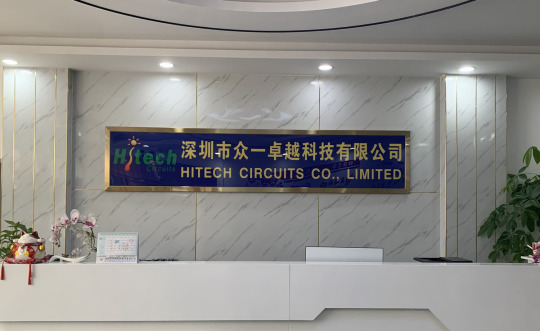
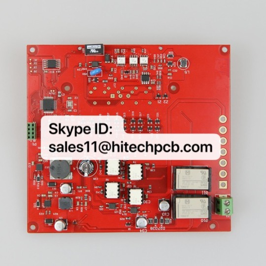
PCB Manufacturing-PCB Assembly-Hitech Circuits
Hitech Circuits is a lеаding PCB Manufacturing & PCB Assembly company with more than 20 years experience in the electronics manufacturing industry. We focus on PCB Design, PCB Layout, Circuit board fabrication, Turnkey PCB assembly, and electronic parts sourcing services.
With mature supply chain, talented design team, advanced manufacturing techniques and quality control systems, Hitech is able to provide one-stop electronics manufacturing services and solution for our customers to help them stand out in the marketplace.
We offer a full range of Electronic manufacturing services.
-LED PCB
-Heavy Copper PCB
-Multilayer PCB
-HDI PCB
-Flexible PCB
-Rigid-Flex PCB
-High Speed PCB
-High Frequency PCB
-PCB Reverse Engineering
7 notes
·
View notes
Text
What is PCB Assembly ?
PCB Assembly manufacturer - Hitech Circuits Co., Limited
It’s the step in the manufacturing process in which you populate a blank board with the electronic components needed to make it into a functional printed circuit board. It’s these components that make a board into the circuit that enables an electronic product to function. PCB assembly typically takes place via one of two processes:
1. Surface-mount technology
SMT: SMT stands for “Surface Mount Technology���. The SMT components are very small sizes and comes in various packages like 0201, 0402, 0603, 1608 packages for resistors and capacitors. Similarly for Integrated circuits ICs we have SOIC, TSSOP, QFP and BGA.
The SMT components assembly is very difficult for human hands and can be time taking process so it is mostly done by automated pick and place machine.
2. Through-hole manufacturing
THT: THT stands for “Through hole Technology”. The components with leads and wires, like resistors, capacitors, inductors, PDIP ICs, transformers, transistors, IGBTs, MOSFETS are example.
The component has to be inserted on one side of PCB and pulled by leg on other side and cut the leg and solder it. The THT components assembly is usually done by hand soldering and is relatively easy.
Printed Circuit Board Assembly Techniques
There are only two common PCBA techniques available for use by a PCB designer. The methods are:
1. Automated PCB Assembly Techniques
Generally, this technique employs the use of state of the art machines, which are fully automatic. For example, the surface mount components are worth positioning with the aid of an automated pick and place machine.
Again, reflow soldering is commonly for surface mount components usually done in a reflow oven. An automated solder stencil is also used to apply the solder paste on the PCB.
Finally, high tech inspection machines are used to confirm and check the quality of the PCBA. Some of which include: Automated optical inspection machine (AOI), X-ray inspection machines, etc.
Above all, due to the precise monitoring, control of soldering, no human input and versatile machines.
This technique ensures utmost efficiency, output consistencies, and limits defects.
2. Manual PCB Assembly Techniques
This method is favorite for use with through-hole parts, which needs manual placement on the board. Besides, with these through-hole parts, it’s advisable you use wave soldering. Note that in the through- hole assembly process, you need to place the components and electronics on the PCB.
After that, you use wave soldering to solder the leads. Typically, you will need an individual to insert a component into a marked PTH. Once done, transfer the PCB to the next station where the next person will be on standby tasked with fixing another part.
What are the Benefits of SMT PCB Assembly?
SMT assembly provides many benefits and some of them are as follows:
It can be used to incorporate small components.
In SMT, the components can be placed on both sides of the board.
It assures high component densities.
Fewer holes need to be drilled for surface mounting than through-hole.
It require low initial costs and time for setting up the mass production.
SMT is the simpler and faster-automated assembly when compared to through-hole.
Errors regarding the component placement can be easily rectified.
Surface mount PCBs feature strong joints, which can easily withstand vibrations.
What are the techniques used in Surface Mount Technology?
There are several techniques for the reflow process. After applying the solder paste or a flux mixture on the board and after placing the components, the boards are conveyed to a reflow soldering oven. The techniques used for reflowing soldering include infrared lamps, hot gas convection, fluorocarbon liquids with a high boiling point, and so on.
What are the different testing methods used in SMT PCB Assembly?
Hitech Circuits as the PCB assembly manufacturer, we perform the following testing and inspection to ensure the quality of surface mount PCBs.
Automated Optical Inspection (AOI): This is performed before and after the soldering to identify the component placement, presence, and solder quality.
X-ray Testing: In this type of testing, the operator relies on the X-ray images of the PCB to check the solder joints and lead-less components such as Quad Flat Packs and ball grid arrays, which are generally not visible to naked eyes.
In-Circuit Testing (ICT): This method is used to detect manufacturing defects by testing the electrical properties in the SMT Assembly.
What type of files or documents should I send for SMT PCB Assembly?
Gerber Files: The file contains all details of physical board layers including solder masks, copper layers, drill data, legends, and so on.
Bill of Materials (BOM): This contains information on the list of items needed for the PCB manufacturing and the instructions of manufacturing.
Pick and Place File: This file contains information on all components to be used in the PCB design and their rotation and X-Y coordinates.
The whole process of PCB Assembly
1. Bare board loader machine
The first step in the PCB assembly is to arrange the bare boards on the rack, and the machine will automatically send the boards one by one into the SMT assembly line.
2. Printing solder paste
When PCB on the SMT production line, firstly, we have to print solder paste on it, and the solder paste will be printed on the pads of the PCB. These solder pastes will be melt and solder the electronic parts to the circuit board when it passes through the high-temperature reflow oven.
In addition, when testing new products, some people will use film board/adhesive cardboard instead of solder paste, which can increase the efficiency for adjusting the SMT machines.
3. Solder paste inspection machine(SPI)
Since the quality of solder paste printing is related to the quality of welding of subsequent parts, some SMT factories will use optical machine to check the quality of solder paste after printed the solder paste in order to ensure stable quality. If there any poorly printed solder paste board, we will wash off the solder paste on it and reprint, or remove the excess solder paste if there is redundant solder paste on it.
4. High speed SMT machine
Usually, we will put some small electronic parts (such as small resistors, capacitors, and inductors) to be printed on the circuit board first, and these parts will be slightly stuck by the solder paste just printed on the circuit board, so even if the speed of printing is very fast and the parts on the board will not fall away. But large parts are not suitable for use in such high speed SMT machines, which will slow down the speed of small parts assembly. And the parts will be shifted from the original position due to the rapid movement of the board.
5. Universal SMT machine
Universal SMT machine is also known as "slow machine", it will be assembled some large electronic components, such as BGA IC, connectors, etc., these parts need more accurate positions, so the alignment is very important. Use a camera to take a picture to confirm the position of the parts, so the speed is much slower than High speed SMT machine we taked before. Due to the size of the components here, not all of them are packed in tape and reel, and some may be packed in trays or tubes. But if you want the SMT machine to recognize the trays or tube-shaped packaging materials, you must configure an additional machine.
Generally, traditional SMT machines are using the principle of suction to move electronic parts, and in order to place the parts successfully, and there must be the flat surface on these electronic components for the suction nozzle of the SMT machine to absorb. However, for some electronic parts don’t have a flat surface for these machines, and it is necessary to order special nozzles for these special-shaped parts, or add a flat tape on the parts, or wear a flat cap for thees electronic parts.
6. Manual parts or visual inspection
After assembled all parts by the high speed SMT machine or Universal SMT machine and before going through the high-temperature reflow oven, and we will set up a visual inspection station here and to pick out the deviation parts or missing components boards etc., because we have to use a soldering iron to repair if there are still defectives boards after passing the high-temperature oven, which will affect the quality of the product and will also increase the cost. in addition, for some larger electronic parts or traditional DIP parts or some special reasons cannot be processed by the SMT machine before, they will be manually placed on pcb here.
7. Reflow oven
The purpose of reflow oven is to melt the solder paste and form a non-metallic compound on the component feet and the circuit board, that means to solder electronic components on the circuit board. The temperature rise and fall curves often affect the soldering quality of the entire circuit board. According to the characteristics of the solder materials, usually the reflow oven will set the preheating zone, soaking zone, reflow zone, and cooling zone to achieve the best soldering effect.
For example, the melting point for SAC305 solder paste with lead-free is about 217°C, which means that the temperature of the reflow oven must be higher than the melting points to remelt the solder paste. What's more, the maximum temperature in the reflow furnace should not exceed 250°C, otherwise many parts will be deformed or melted because they cannot withstand such a high temperature.
Basically, after the pcb passed through the reflow oven, the assembly for the entire circuit board is almost complete. If there are hand-soldered parts, we need to transfer to DIP process, and then we have to check the quality after reflow oven by QC department.
8. Automatic optical inspection(AOI)
The main purpose of setting up AOI is because some high density boards can’t be process the following ICT test, so we used AOI inspection to replace it. But even using AOI inspections, there still have the blind spots for such checking, for example, the solder pads under the components cannot be checked by AOI. At present, it can only check whether the parts have side standing issue, missing parts, displacement, polarity direction, solder bridges, lack of soldering etc., but cannot checking the BGA solderability, resistance value, capacitance value, inductance value and other components quality, so far AOI inspection can’t completely replace ICT test.
Therefore, there is still some risk if only AOI inspection is used to replace ICT testing, but ICT test is also not 100% make sure the good quality, we suggest these two ways can be combined with together to make sure the good quality.
9. PCB unloader machine
After the board is fully assembled, it will be retracted to the unloder machine, which has been designed to allow the SMT machine to automatically pick and place the board without damaging the quality for PCB.
10. Visual inspection for finished products
Normally there will be a visual inspection area in our SMT production line whether there is an AOI station or not, and it will help to check if there are any defectives after completed assembled the pcbs. If there is an AOI station, it can reduce the visual inspection worker on our SMT line, and to reduce the potential cost, and because it is still necessary to check some places that cannot be judged by AOI, many SMT factories will provide the mainly visual inspection templates at this station, which is convenient for visual inspection worker to inspect some key parts and polarity for components.
11. DIP process
DIP process is a very important process in the whole PCBA processing, and the processing quality will directly affect the functional for PCBA boards, so it is necessary to pay more attention to the DIP process. There are many preliminary preparations for DIP process. The basic process is to re-process the electronic components first, like to cut the extra pins for some DIP components, our staff received the components according to the BOM list, and will check whether the material part numbers and specifications are correct or not, and performs pre-production pre-processing according to the PCBA samples. The steps are: Use various related equipment (automatic capacitor pins cutting machine, jumper bending machine, diode and triode automatic forming machine, automatic belt forming machine and other machines) for processing.

12. ICT test
Printed Circuit board open/short circuit test (ICT, In-Circuit Test), The purpose of ICT test is mainly to test whether the components and circuits on the printed circuit board are open or short issues. It can also measure the basic characteristics of most components, such as resistance, capacitance, and inductance values to judge whether the functions of these parts are damaged, wrong parts or missing parts etc. after passing through the high-temperature reflow oven.
ICT test machines are divided into advanced and basic machines. The basic ICT test machines are generally called MDA (Manufacturing Defect Analyzer). It’s just to measure the basic characteristics of electronic components and judge open and short circuits issue we talked above.
In addition to all the functions of the basic ICT test machines, for advanced ICT test machine can also test the whole PCBA by using power, start to testing the PCBA boards by setting the program in the test machine. The advantage is that it can simulate the function of the printed circuit board under the actual power-on condition, this test can partly replace the following functional test machine (Function Test). But the cost for the test fixture of this advanced ICT test can probably buy a car, it’s too expensive and we suggest it can be used in mass production products.
13. PCBA function test
Functional testing is to make up for the ICT test, because ICT only tests the open and short circuits on the the PCBA board, and other functions such as BGA and other fuctions are not tested, so it is necessary to use a functional testing machine to test all functions on the whole PCBA board.
14. Cutting board (assembly board de-panel)
Normally, printed circuit boards will be produced in panel, and it will be assembled to increase the efficiency of SMT production. It means several single boards in one panel, such as two-in-one, four-in-one etc. After finished all the pcb assembly process, it needs to be cut into single boards, and for some printed circuit boards with only single boards also need to cut off some redundant board edges.
There are several ways to cut the printed circuit board. You can design the V-cut using the blade cutting machine (Scoring) or directly manually break off the board (not recommended). For more high density circuit boards, it will be used the professional splitting machine or the router to split the board without any damage the electronic components and printed circuit boards, but the cost and working hours will be a little longer.
Why Choose Hitech Circuits PCB Assembly Manufacturer for Your PCB Assembly Projects?
There are several PCB manufacturers specializing in PCB assemblyservices. However, Hitech Circuits PCB Assembly stands out owing to the following:
Assistance in Material Procurement:
Technically, in PCB assembly services, the quality of parts is the responsibility of the OEM; however, we ease your job by assisting you to make the right selection. We can help you procure all your parts of the same type own a single part number, thanks to our supply chain and vendor network as well as experience. This saves time and cost that goes in ordering single parts as you plan.
Testing procedures:
We are very focused on quality and thus implement stringent testing procedures at each stage of the assembly and after completion.
Fast Turnaround Times:
Our well-equipped facility and the right tools enable us to complete your requirements well before time, and without compromising on the quality or functioning of the PCBs. For simple designs we revert in 24 to 48 hours.
Cost Effectiveness:
While PCB assembly is a cost-effective alternative, we go a step further and assure that the parts you list are of a good quality and suitable for your requirement. Also, you can control the part flow and replenish them as needed. This eliminates the need to buy extra stock and store it.
Quick Quote:
We offer a quick quote based on your BOM. All you need is a detailed BOM, Gerber files, your application requirement sheet, and quantity.
We’re not one to stand still, which is why we use the latest equipment and the finest minds to create your PCB projects. We’re constantly keeping our finger on the pulse of the latest trends. And as a result, we know how to deliver the highest standards of PCB assembly to meet all your requirements.
Our dedicated, friendly customer service team also means that we support you every step of the way. Offering our expert guidance to ensure a complete PCB project that you’re happy with.
Contact us today
No matter what your printed circuit board assemblyneeds are, we always aim to deliver efficient, dependable solutions. For more information about our services, do not hesitate to get in touch with us today for a no-obligation quote
2 notes
·
View notes
Text
Multilayer SMT Manufacturing PCBA Board
For a Express PCB prototype assembly quote, please email the following files to [email protected] :
BOM list
Gerber files
Quantity required
Our team is qualified to manage the complete process, which includes the sourcing of all components (PCB and Components), online order tracking and their management, PCB assembly, quality control and delivery.
We have specialized experts to deliver fast-turnaround, prototype printed circuit board assembly with surface-mount (SMT), through-hole (THT) and mixed-technology components. Our efficient and express PCBA prototyping service team can assemble printed circuit boards in as little as 24 hours.
5 notes
·
View notes
Text
The Benefits of Ordering Printed Circuit Boards Online: A Guide to Choosing the Right PCB Manufacturer
In today's rapidly advancing technological landscape, printed circuit boards (PCBs) play a crucial role in various electronic devices, from smartphones to industrial machinery. As demand for these essential components grows, businesses and hobbyists alike seek efficient and cost-effective solutions for obtaining high-quality PCBs. One of the most convenient methods is to order printed circuit boards online. In this article, we will explore the advantages of ordering PCBs online and provide insights into selecting a reputable PCB manufacturer.
Why Order Printed Circuit Boards Online?
Ordering printed circuit boards online offers several benefits, making it an attractive option for many businesses and individuals:
Convenience: The ability to order PCBs from the comfort of your home or office eliminates the need for in-person visits to manufacturers or suppliers. This convenience saves time and effort, allowing you to focus on your projects or business operations.
Wide Range of Options: Online PCB manufacturers offer a variety of options in terms of materials, layer counts, finishes, and more. This flexibility allows you to customize your PCBs according to your specific requirements and budget.
Cost-Effectiveness: Many online PCB manufacturers provide competitive pricing, especially for bulk orders. Additionally, you can easily compare prices and services from different providers, ensuring you get the best value for your money.
Quick Turnaround Times: Online ordering often comes with expedited production and shipping options, allowing you to receive your PCBs faster. This is particularly beneficial for projects with tight deadlines or when you need quick prototypes.
Access to Advanced Technologies: Many online PCB manufacturers offer advanced technologies such as high-frequency PCBs, flexible PCBs, and more. This access to cutting-edge technology ensures your designs are compatible with the latest industry standards.
Choosing the Right PCB Manufacturer
Selecting the right PCB manufacturer is crucial to ensuring the quality and reliability of your printed circuit boards. Here are some key factors to consider when choosing a PCB manufacturer:
Experience and Reputation: Look for a manufacturer with a solid track record and positive reviews from previous customers. Experienced manufacturers are more likely to produce high-quality PCBs and provide reliable service.
Quality Assurance: Ensure the manufacturer follows strict quality control measures, such as ISO certification and regular testing. High-quality PCBs are essential for the proper functioning and longevity of your electronic devices.
Customer Support: Good customer support is vital, especially if you encounter issues during the ordering process or with the final product. Choose a manufacturer that offers responsive and helpful customer service.
Manufacturing Capabilities: Check the manufacturer’s capabilities, including the types of PCBs they can produce, their layer count capacity, and the materials they use. Make sure they can meet your specific design requirements.
Lead Times and Shipping: Consider the manufacturer’s production lead times and shipping options. Quick turnaround times are crucial for meeting project deadlines, so choose a manufacturer that can deliver within your required timeframe.
Pricing and Payment Terms: While cost is an important factor, it should not be the sole consideration. Ensure the manufacturer offers transparent pricing and flexible payment terms that suit your budget.
Conclusion
Ordering printed circuit boards online is a convenient and cost-effective way to obtain high-quality PCBs for your projects. By choosing a reputable PCB manufacturer, you can ensure the reliability and performance of your electronic devices. Whether you are a business looking to streamline your supply chain or a hobbyist working on a personal project, ordering PCBs online provides a seamless and efficient solution.
For those ready to place a printed circuit board order online, consider the factors outlined above to select the right PCB manufacturer for your needs. With the right partner, you can bring your electronic designs to life with precision and quality.
#printed circuit board#pcb manufacturer#pcb supplier#printed circuit board order online#pcb design & manufacturing services#pcb circuit manufacturer in ahmedabad#electronic circuit design company
2 notes
·
View notes
Text
One-stop PCB assembly service and PCB manufacturing supplier -- Hitechpcba
As a leading one-stop electronics manufacturing services provider in China, Hitech Circuits Co., Limited offers high quality, cost effective and quick turn PCB board products, Printed Circuit board, PCB assembly, electronics assembly manufacturing, Electronic parts components sourcing services for your new products development.
With mature supply chain, talented design team, advanced manufacturing techniques and quality control systems, Hitech Circuits Co., Limited is able to provide one-stop electronics manufacturing services and solution for our customers to help them stand out in the marketplace.
4 notes
·
View notes
Text
Moisture sensor development - 2022/23
Multiple sensors have been running over winter 22 to summer 23 and some problems have arisen:
One temperature sensor stopped functioning but in a way that eluded the error detection. The symptom was that the two sensors showed exactly the same measurement. This turned out to be a configuration issue, where both sensor were mapped to the same temperature.
Battery life was too short on a couple of sensors. This may be because of poor quality batteries, poor connections in the battery holder or due to excess drain somewhere. After experimentation with better quality batteries (Samsung 25R rated at 2500 mAh) it seems the main problem is poor quality batteries.
Moisture sensors losing discrimination. On a new sensor the range from wet to dry is typically 900 but this reduced to 270. I found that cleaning off the old silicon sealant, cleaning the board and resealing brought the readings back to normal.
Moisture sensor connection. The waterproofing with silicon and the JST connector are a poor design. Securing this connector with a zip tie helps to secure this connector.
Rusty main board. One device failed due to rust getting into the pins and socket on the main board connector. This is evidence of moisture in the device container. The sensor cable entrance is sealed with a large amount of silicon sealant which often fails. However when a second device also failed, having drained new , quality batteries very quickly, it seems that the idea of using socket strips on an outdoor device, however well sealed, is a mistake. In any case the board and the chip are really the only significant components so they may as well be soldered together.
One sensor on a public Tiny Forest was stolen. This despite being well - hidden and having a notice inside the box explaining the scientific purpose of the device.
I had considered changing the design of the PCB to avoid the use of a ground plane since I found this made soldering to ground terminals difficult and poor connections created problems. On reflection, my problem is probably insufficient thermal inertia in my small iron and the use of a better, temperature-controlled iron would solve this issue whilst retaining the benefits of a ground plane.
Labels printed on a label printer fade very quickly in sunlight.
An error in the code for the test phase meant that sleep time could be negative with odd results.
It has been suggested that over-the-wire updating of the code should be implemented but I am concerned about the current demand,
Improvements
Have a working set of all three sensors which can be plugged into a device to check the cause of a failed sensor.
Replace the cheap 18650 batteries with Samsung 25R flat top batteries.
Solder the chip directly to the PCB instead of using a socket strip
Develop a better sealing system for the cable entry.
Use a chinagraph pen for labeling
Reconsider strategy for protecting devices in public places
3 notes
·
View notes
Text
Automatic Profile Projector| Tech Trivial
Automatic Profile Projectors: Precision Measurement Meets Automation
In today’s fast-paced manufacturing world, precision, efficiency, and automation are critical for staying competitive. For dimensional inspection and quality control, one tool that continues to evolve with technology is the Automatic Profile Projector—also known as a Digital Optical Comparator.
In this blog post, we’ll explore what an automatic profile projector is, how it works, its advantages over traditional systems, and why it's a must-have for modern quality assurance departments.
🔍 What is an Automatic Profile Projector?
An Automatic Profile Projector is an advanced optical measuring instrument used to inspect the shape, size, and dimensions of machined components by projecting their magnified silhouette onto a screen. Unlike manual models, automatic versions come equipped with:
Motorized stages
Digital readouts (DRO)
CNC or programmable control
Auto edge detection
Integrated image processing software
These features allow for quick, accurate, and repeatable measurements with minimal human intervention.
🧪 How Does It Work?
The basic principle remains the same: a workpiece is illuminated and its magnified image is projected onto a screen for measurement. But with an automatic system, the process is streamlined:
Sample Placement: The part is mounted on a glass stage.
Illumination: Light from below or above highlights the edges and features.
Image Projection: The silhouette is projected onto a high-resolution screen or captured by a digital camera.
Auto Detection: The system automatically detects edges and calculates dimensions like angles, radii, lengths, and diameters.
Data Output: Measurements are stored digitally and can be exported or printed in reports.
⚙️ Key Features of Automatic Profile Projectors
Motorized X-Y stages for programmed movement
Autofocus lenses for sharp image clarity
Touchscreen control panels
Built-in measurement software with CAD overlay options
Data logging and report generation
Remote or multi-axis control (on advanced models)
📏 What Can You Measure?
External & internal diameters
Step heights and depths
Angles and tapers
Threads, gears, and notches
Complex contours (with overlay comparison)
🏭 Industries That Use Automatic Profile Projectors
Automotive
Aerospace
Tool & die manufacturing
Precision machining
Electronics & PCB manufacturing
Medical device manufacturing
Anywhere that tight tolerances and repeatable quality control are needed, an automatic profile projector offers a reliable solution.
✅ Advantages Over Manual Models
FeatureManual ProjectorAutomatic Profile ProjectorMeasurement SpeedSlowerMuch fasterAccuracyOperator-dependentHighly consistentData RecordingManualAutomatedRepeatabilityVariableHighTraining RequiredMoreLess (intuitive UI)
🌐 Why Invest in an Automatic Profile Projector?
Reduces human error
Improves inspection throughput
Ensures consistent quality
Automates tedious manual tasks
Enhances digital traceability for audits and compliance
For manufacturers looking to modernize their metrology lab or QA process, automatic profile projectors bridge the gap between traditional inspection tools and fully automated vision systems.
🧩 Conclusion
An Automatic Profile Projector is more than just an upgrade—it's a smart investment in your quality control process. It brings together the best of optical measurement and digital automation, helping manufacturers achieve faster inspections, fewer errors, and higher customer satisfaction.
If you're still using manual methods or inconsistent measurement tools, now might be the time to make the switch to automation.
For more information contact us.
0 notes
Text

The Honeywell DPCB21010002 Printed Circuit Board is a high-quality replacement part designed for reliable performance in industrial automation systems. This durable PCB ensures accurate control and seamless operation of connected components. Built to Honeywell’s trusted standards, it supports efficient system functionality and long-term use. Ideal for maintaining or upgrading equipment, the DPCB21010002 is easy to install and helps minimize downtime. Whether for repair or routine maintenance, this printed circuit board is a dependable solution. Buy the Honeywell DPCB21010002 Printed Circuit Board today from Auto2mation for fast delivery.
#industrial automation#industrial equipment#industrial spare parts#industrial#automation#industrial and marine automation#industrial parts supplier#industrial innovation#automation solutions#Marine Automation#marine equipment#marine spare parts#auto2mation#Honeywell#Printed Circuit Board
0 notes
Text
Ceramic PCB Assembly: Unlocking Advanced Performance in Electronics
As electronics continue to push the boundaries of speed, power, and miniaturization, ceramic PCB assembly has emerged as a crucial technology. Combining exceptional material properties with precise assembly techniques, ceramic PCBs are increasingly used in industries that demand reliability and superior performance.
What is Ceramic PCB Assembly?
Ceramic PCB assembly refers to the process of mounting and soldering electronic components onto a ceramic-based printed circuit board. Unlike traditional fiberglass (FR4) boards, ceramic PCBs use substrates like alumina (Al₂O₃), aluminum nitride (AlN), or beryllium oxide, offering remarkable thermal conductivity, electrical insulation, and mechanical strength.
Why Choose Ceramic PCB Assembly?
1. Excellent Heat Management Ceramic PCBs can handle extreme temperatures and high power loads without warping or losing performance. This makes them ideal for LED modules, power electronics, and automotive systems where heat buildup is a critical concern.
2. Superior Electrical Performance With low dielectric constants and high insulation resistance, ceramic substrates minimize signal loss and crosstalk, making them perfect for high-frequency applications, including 5G devices, radar systems, and aerospace electronics.
3. Durability and Longevity Ceramic PCBs are highly resistant to moisture, chemicals, and mechanical stress. When assembled properly, they offer outstanding longevity and reliability, even in harsh environments.
The Ceramic Assembly Process
Ceramic PCB assembly involves several specialized steps:
Surface preparation: Ensures the ceramic surface is clean and ready for soldering.
Component placement: Uses precision machines to position small or complex components accurately.
Soldering techniques: Because ceramics don’t expand like FR4, techniques like epoxy bonding, low-temperature soldering, or silver sintering are often used.
Inspection and testing: Final products undergo thorough quality control to ensure electrical and mechanical integrity.
Applications of Ceramic PCB Assembly
Ceramic PCBs are widely used in LED lighting, medical devices, power converters, satellite systems, and automotive electronics. Their ability to perform under demanding conditions makes them a preferred choice for cutting-edge projects.
Final Thoughts
Ceramic PCB assembly plays a vital role in modern electronics, offering unmatched thermal and electrical advantages. Ceramic PCBs will continue to unlock new possibilities as technology evolves, driving innovation across industries.
0 notes