#FPGA Synchronization
Explore tagged Tumblr posts
Visit Tumblr Blog
Explore Tumblr blogs with no restrictions, modern design and the best experience.
Last Seen Tumblr Blogs


Fun Fact
Tumblr.com rank in the US is 25.
Text
The Tick Data Arms Race: How Institutions Stay Ahead
Decoding the Market's DNA: What Tick Data Reveals
Tick data isn't just about speed - it's about seeing the market's hidden structure. Consider these insights available only at tick-level resolution:
Order Flow Imbalances
Detect when buy/sell pressure reaches critical thresholds
Example: A sudden 5:1 buy/sell ratio in 10ms often precedes 0.5% price jumps
Liquidity Shadows
Identify "ghost liquidity" - large orders that appear/disappear rapidly
python复制下载def detect_ghost_liquidity(order_book): return (order_book['bid_size_changes'] > 500%) & (order_book['cancel_rate'] > 80%)
Market Maker Footprints
Recognize algorithmic patterns used by institutional liquidity providers
Key markers:
Symmetrical order placement
Micro-adjustments (0.01% price changes)
Millisecond-level response times
Building Your Tick Data Toolkit
Hardware Essentials
ComponentMinimum SpecIdeal SetupProcessor4-core CPU8-core+ with AVX-512RAM16GB DDR464GB+ DDR5StorageSATA SSDNVMe Gen4 (7GB/s+)Network1Gbps10Gbps dedicated line
Pro Tip: For Bitcoin trading, add FPGA acceleration to handle SHA-256 calculations at wire speed.
Software Stack
Data Collection Layer
Use Kafka or Redpanda for real-time stream processing
Implement data compression (Zstandard) to reduce storage needs by 70%
Analysis Enginepython复制下载from tensorflow.keras import layers model = Sequential([ layers.LSTM(128, input_shape=(1000, 15)), # 1000 ticks, 15 features layers.Attention(), layers.Dense(3, activation='softmax') # Buy/Hold/Sell ])
Execution System
Nanosecond timestamp synchronization (PTP protocol)
TCP bypass for order entry (kernel-level networking)
Case Study: Catching the Flash Crash
During the May 2023 crypto crash, traders using our recommended setup:
Spotted liquidity withdrawal 47ms before major price drop
Triggered short positions at 0.5% below market
Captured 18% returns while others faced 30% losses
Key Indicators They Monitored:
Derivatives funding rate divergence
Stablecoin redemption spikes
Order book "thinness" index
The Future of Tick Trading
Emerging technologies set to disrupt the space:
Quantum Order Routing
Tested by Jump Trading, reduces latency to 5 nanoseconds
Neuromorphic Chips
Brain-inspired processors that learn market patterns organically
Decentralized Data Markets
Blockchain-based tick data exchanges (e.g., Pyth Network)
Your Action Plan
Start with a focused market (e.g., BTC/USD)
Build basic anomaly detection models
Gradually add complexity as your infrastructure improves
Remember: In high-frequency trading, every microsecond saved is worth approximately 0.02per0.02per1M traded (NYSE estimate).
Register for [Alltick.co] and unlock the full potential of tick data—truly "stay one step ahead" in your trading strategies!
1 note
·
View note
Text
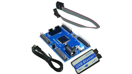
ECE 3544: Digital Design I Project 3 (Part B) – Design and Synthesis of a Synchronous Finite State Machine
In this project, you will take an existing synchronous finite state machine module and modify it to add features. You will implement your top-level module on the Altera DE1-SoC board, so you will gain practice with assigning pins of your FPGA to the module’s input and output ports, and with synthesizing modules. Requirements The DE1-SoC board IS REQUIRED for this project. You must have the…
0 notes
Text
Elmalo, let's move forward with scoping a full pilot buildout—starting with the v1 Mars Habitat Monitor. This path offers a compelling, high-stakes testbed for the Iron Spine system and allows us to prototype under extreme, failure-intolerant conditions. Designing for Mars pushes the architecture to its limits, ensuring resilience, autonomy, and layered intelligence from the outset.
🚀 v1 Mars Habitat Monitor – Pilot Buildout
🔧 Environmental Design Requirements
Radiation-Hardened Components: Select radiation-tolerant MCU/FPGA and sensor components (e.g., RAD750 derivatives or Microsemi FPGAs).
Thermal Regulation: Passive and active methods (phase-change materials, aerogels, thin-film heaters).
Dust Protection: Hermetically sealed enclosures with electrostatic or vibrational dust mitigation (similar to the Mars 2020 rover’s approach).
Power Constraints: Solar panels + supercapacitors for charge buffering, with ultra-low power idle modes.
Communications Delay Tolerance: Incorporate DTN (Delay-Tolerant Networking) bundles for relayed Earth-Mars messaging.
🧠 Sensor Suite
Life Support Monitoring:
CO₂ / O₂ / CH₄ levels
Humidity / Temperature / Pressure
Structural Integrity:
Microfracture sensors (piezo-acoustic or fiber optic strain gauges)
Vibration analysis (accelerometers/IMUs)
Radiation Exposure:
Ionizing radiation detectors (Geiger-Müller tubes or RADFETs)
Environmental:
Dust density (LIDAR or IR scattering)
UV exposure, ambient EM fields
🧩 System Architecture
Sensor Synchronization:
Use local PTP clocks with oscillator drift correction from a central unit
Redundant clocks for fault detection
Data Fusion Layer:
Edge-level Kalman filters for each sensor type
Onboard anomaly detection with TensorRT-lite or ONNX models for pattern deviation
Edge Inference:
PyTorch Mobile or ONNX on an ARM-based SOM (e.g., NVIDIA Jetson Nano with radiation shielding)
Data Relay and Storage:
Store all telemetry in redundant onboard buffers
Use prepackaged DTN bundles and error-correcting transmission protocols to transmit during windowed comms
Digital Twin Integration:
Each monitor syncs with a simulated Mars habitat replica in Earth orbit or ground control
Dashboard via Prometheus/Grafana or a bespoke Unity/Unreal-powered 3D monitoring console
⚙️ Resilience & Power
Watchdog Timers: Auto-reset on failure, with a secondary power rail for minimal heartbeat signal
Power Monitoring: Real-time tracking of draw, supercapacitor status, and solar charge
Failover States: Downgraded functionality tier for power preservation and sensor core redundancy
Would you like a modular breakdown of the above, suitable for PCB design, mechanical housing, and software stack implementation? Or perhaps a visual mission profile that tracks expected operational phases, anomaly response, and maintenance cycles for the Mars system?
Let’s make this pilot the template for Iron Spine’s interplanetary leap.
0 notes
Text
Laboratory 7 – Simple VGA Driver to Display 256 Different Colors
This project is part of the course ‘Digital System Design Lab’. The purpose of this lab is to design a VGA driver to display 256 different colors on a monitor. The color data of each pixel is generated using an 8 bit counter implemented on an FPGA board. Description The VGA driver project generates two timing signals, `vsync` and `hsync`, to synchronize the plotting of vertical and horizontal…
0 notes
Text


GB8002 RACK-MOUNT HIGH PRECISION BEIDOU/GPS NTP TIME SERVER GB8002 high precision BeiDou / GPS time server is developed by our company based on GPS timing technology device. It can display and send standard time. The time server uses the PPS and time message of BeiDou Navigation System and GPS (Global Positioning System) satellite to output time synchronization pulse. The device uses SMT surface mount technology for production and high-speed chip for control, with high precision, high stability, strong function, no accumulative error, cost-effective and easy to operate. It is also not limited by geographical and climatic conditions. The device can be widely used in electric power system, network synchronization, communication, traffic management and national defense need timing and punctuality etc. The device has a variety of interfaces. such as RJ45, RS-232, RS-422/RS-485, IRIG-B, TTL Pulse etc. Multi-channel output pulses such as seconds, minutes and hours (free translation), convenient connections and related device, implements unidirectional or bi-directional communication.
FEATURES ■ Provide programmable TTL pulse, can be set to PPS, PPM and PPH, flexible and convenient. ■ 1U Frame structure ,19 inch standard chassis, easy installation and maintenance. ■ All-weather signal coverage to ensure long-term continuous high-reliability high-precision timing. ■ All signal input and output interfaces are photoelectric isolation measures, safe and reliable. ■ High performance, wide range switching power supply, AC-DC compatible input, convenient and reliable, stable operation. ■ Satellite signal receiving and self-service hot standby, according to priority automatically select clock source, seamless switching. ■ The 32-bit high-speed microprocessor + large-scale integrated FPGA chip, parallel high-speed data processing and various codes, excellent performance. ■ Separate 10 M/100M network ports (each port has a separate MAC address), flexible configuration, can be used in different sub-nets or different physical isolation networks, using NTP/SNTP protocols to provide time synchronization services. ■ High-precision punctuality frequency is derived from adaptive synchronization technology, closed-loop control punctuality technology to tame constant temperature crystal oscillator, to achieve long-time high-precision punctuality. ■ Central master clock has 1 channel pulse ,10 channels B code ,3 channels 232 serial port ,3 channels 485 serial port ,2 channels Ethernet. ■ Optional GPS or BeiDou or CDMA three satellite receiving modes, high signal strength, local distributed installation is convenient. Especially suitable for communication base station, power plant, substation, machine room and other equipment time synchronization.
APPLICATION ■ Power plant; ■ Airport time system; ■ Hospital time system; ■ Electric power system; ■ Traffic management system; ■ Radio and television system; ■ Financial insurance company; ■ Network time synchronization; ■ Mobile communication system; ■ Petrochemical iron and steel enterprises;
0 notes
Text
0 notes
Text
Register Datasheet: The Power of Smart Datasheet Management

In today’s data-driven world, the efficiency with which we manage and access information plays a pivotal role in success, especially in industries dealing with vast amounts of data. A register datasheet, or more broadly, a smart datasheet, provides an innovative solution to streamline data handling, improve accessibility, and reduce manual errors. These smart datasheets have revolutionized traditional data management systems by embedding dynamic features and ensuring a high level of adaptability for modern businesses. This article explores the concept of a register datasheet, its features, advantages, and its significance in today’s digital landscape.
What is a Register Datasheet?
A register datasheet refers to a document that lists and defines all the internal and external registers associated with a hardware device, such as a microcontroller or an FPGA (Field Programmable Gate Array). These registers store critical control data, configuration settings, and real-time operational information, enabling the device to function optimally. Traditional register datasheets were static, often in the form of PDFs or spreadsheets, that engineers and developers would use for reference during system design, development, and troubleshooting.
However, as systems have grown more complex, the demand for more smart datasheets has increased. A smart datasheet is an advanced digital version of a traditional datasheet. It’s interactive, dynamic, and integrated with automated functionalities, allowing for real-time updates, searchability, and easy data manipulation.
Features of a Smart Register Datasheet
Interactive Interface: A smart datasheet offers a user-friendly, interactive interface. Instead of scrolling through endless pages of static data, users can click through sections, filter specific details, or jump to relevant data points instantly.
Real-Time Updates: Unlike traditional datasheets that require manual updates, smart datasheets integrate directly with the data source, ensuring that all information remains up-to-date in real time. For instance, when a new hardware version or firmware update is released, the smart datasheet reflects the changes immediately.
Search and Filter Capabilities: Smart datasheets allow users to search for specific registers or configuration options quickly. Advanced filter options let users narrow down to relevant data, saving time and reducing human error when interpreting or extracting data.
Data Visualization: Visual aids such as charts, graphs, and diagrams are embedded directly into the smart datasheet. These visual representations help engineers better understand the data, track device performance, and compare configurations.
Export and Import Functions: Users can export sections or the entire datasheet into various formats (CSV, XML, PDF) for further analysis. Additionally, smart datasheets allow importing external data to match configurations or perform comparative analysis with existing systems.
API Integration: Smart datasheets often come with API (Application Programming Interface) support, allowing external software or tools to interact directly with the datasheet, retrieve specific data, or push updates.
Advantages of Smart Datasheets
Enhanced Efficiency and Productivity: The interactive nature of smart datasheets reduces the time spent on searching, interpreting, and analyzing data. Engineers no longer need to comb through pages of static text but can access the exact data they need within seconds. This efficiency improves overall productivity, especially in fast-paced environments where timely access to information is crucial.
Improved Accuracy: Manual handling of datasheets often leads to errors, such as misreading registers or applying outdated configuration settings. Smart datasheets eliminate these risks by ensuring all data is accurate and updated automatically. With real-time synchronization, there is no risk of working with outdated specifications.
Customization and Flexibility: Smart datasheets allow for greater customization, enabling users to view data in a format that suits their specific requirements. Whether it’s a specific device configuration, register layout, or operational data, users can tailor the datasheet view to suit their needs. This flexibility makes it easier to manage complex data and adapt to changing project requirements.
Collaboration and Sharing: Smart datasheets enable easy sharing and collaboration among teams. Cloud-based smart datasheets allow multiple users to access, update, or comment on the document in real time. This collaborative approach improves communication within teams and across departments, ensuring everyone is working with the latest and most accurate data.
Integration with Development Tools: Modern smart datasheets integrate seamlessly with development environments and tools such as Integrated Development Environments (IDEs), simulators, or test benches. This tight integration allows engineers to test configurations, simulate behavior, or verify performance directly from the datasheet, enhancing the development workflow.
Importance in the Digital Age
In the era of IoT, AI, and advanced automation, hardware devices are becoming increasingly sophisticated. As a result, the datasheets associated with these devices are more detailed and complex than ever before. Traditional static datasheets simply can't keep pace with the rapid development cycles and growing complexity of modern devices.
Smart datasheets address this challenge by providing dynamic, real-time access to critical data in a format that is both flexible and easy to use. This ensures that engineers and developers have the tools they need to make informed decisions, minimize errors, and accelerate time to market.
Moreover, as remote work and digital collaboration become more prevalent, cloud-based smart datasheets ensure that all stakeholders, regardless of location, have access to the latest data, facilitating better coordination and decision-making.
Conclusion
The register datasheet has evolved from a simple static reference document into a powerful, smart tool for managing complex data. With its interactive interface, real-time updates, search capabilities, and seamless integration, a smart datasheet provides significant advantages in terms of efficiency, accuracy, and collaboration. As industries continue to embrace digital transformation, adopting smart datasheets will become increasingly essential for businesses looking to stay ahead in a competitive, data-driven landscape.
0 notes
Text

Designing a wearable night vision camera is a complex task, particularly when the device must be lightweight, compact, and power-efficient while meeting stringent military standards. The camera needed to integrate two distinct imaging sources — an infrared camera and a low-light camera — to provide superior night vision in challenging environments. The integration of these sources presented a significant challenge. The camera had to process and synchronize high-speed signals from both cameras despite their differing resolutions. This required an advanced FPGA (Field Programmable Gate Array) design capable of managing high-speed parallel processing and video synchronization within the compact confines of a wearable device.
Source - https://volersystems.medium.com/wearable-night-vision-leveraging-fpga-design-for-next-gen-military-applications-66957d806219
#fpga design#fpga devlopment#Electronics Design Services#Electronics Design Company#Electronic Product Design#Electronic Design Services
1 note
·
View note
Text
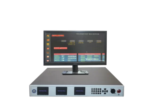
Telemetry Receiver from Digilogic Systems
Digilogic Systems Telemetry receiver design is highly flexible and provides comprehensive link support for satellite and flight test ground station applications in a fully integrated package. Digilogic Systems Telemetry Receiver design features FPGA based signal processing and software defined radio technology in the form of digital telemetry receivers, waveform & signal processors.
A variety of configurations (Single, Dual) and waveforms(AM, FM, PM, BPSK, QPSK & SOQPSK) are available with standard data rates from 40 Mbps down to 100 kbps. It also supports Automatic Gain Control, AM Tracking, Diversity Combining, Equalization, Demodulation of PCM-FM & SOQPSK-TG, Bit Synchronization, Frame Synchronization, LDPC and Convolutional Decoding, and Telemetry Over IP (TMoIP) as per IRIG Standard.
Digilogic Systems Telemetry Receiver system also has an in-built test signal generator, to test the performance of complete receiver chain without any external source. The system also provides access to down converted IF signals, Bit sync outputs, Data & Clock signals for analysis with any external systems. All these I/Os are available through connectors on rear side of the unit. As the system design is indigenous & FPGA based, any kind of customization needed towards any new modulation schemes can be incorporated in the system.
Contact us today to discuss your Telemetry Receiver requirements: website: https://www.digilogicsystems.com/ Phone: Hyderabad: (+91) 40 4547 4601 / 02 / 03 Bengaluru: (+91) 80 4975 6034 Email: [email protected] Locations: HEAD OFFICE
102, 1st Floor, DSL Abacus Tech Park Beside DSL Virtue Mall, Uppal, Hyderabad, Telangana-500 039, India
BRANCH OFFICE
216, 3rd floor, Zareen Heights, Varthur Road, Nagavarapalya, C. V. Raman Nagar, Bengaluru, Karnataka — 560093
0 notes
Text
Analog Devices HMCAD1511TR Comprehensive Guide
Analog Devices HMCAD1511 High Speed Multi-Mode 8-Bit 30 MSPS to 1 GSPS A/D Converter
General Description
The HMCAD1511 is a versatile high performance low power analog-to-digital converter (ADC), utilizing time-interleaving to increase sampling rate. Integrated Cross Point Switches activate the input selected by the user.
In single channel mode, one of the four inputs can be selected as a valid input to the single ADC channel. In dual channel mode, any two of the four inputs can be selected to each ADC channel. In quad channel mode, any input can be assigned to any ADC channel.
An internal, low jitter and programmable clock divider makes it possible to use a single clock source for all operational modes.
The HMCAD1511 is based on a proprietary structure, and employs internal reference circuitry, a serial control interface and serial LVDS/RSDS output data. Data and frame synchronization clocks are supplied for data capture at the receiver. Internal 1 to 50X digital coarse gain with ENOB > 7.5 up to 16X gain, allows digital implementation of oscilloscope gain settings. Internal digital fine gain can be set separately for each ADC to calibrate for gain errors.
Various modes and configuration settings can be applied to the ADC through the serial control interface (SPI). Each channel can be powered down independently and data format can be selected through this interface. A full chip idle mode can be set by a single external pin. Register settings determine the exact function of this pin.
HMCAD1511 is designed to easily interface with Field Programmable Gate Arrays (FPGAs) from several vendors.

Key Features and Specifications
Multi-Mode Operation:
· Single Channel Mode: Maximum sampling rate of 1000 MSPS
· Dual Channel Mode: Maximum sampling rate of 500 MSPS
· Quad Channel Mode: Maximum sampling rate of 250 MSPS
Performance Highlights:
· Signal-to-Noise Ratio (SNR): Up to 49.8 dB in single channel mode
· Power Dissipation: Ultra-low at 710 mW including I/O at 1000 MSPS
· Start-Up Time: 0.5 µs from sleep and 15 µs from power down
Integration and Control:
· Integrated cross-point switches (MUX array) for flexible input selection
· Internal low jitter programmable clock divider
· Digital gain control from 1X to 50X with no missing codes up to 32X
· Serial LVDS/RSDS output for high-speed data transfer
Power and Environmental Specifications:
· Operating Voltage: 1.8V supply voltage
· Logic Levels: 1.7–3.6V CMOS logic on control interface pins
· Operating Temperature: -40°C to 85°C
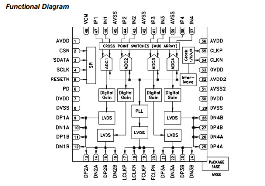
Compatible Electronic Component Series
To maximize the functionality and performance of the HMCAD1511TR, it is essential to pair it with compatible electronic components. Here are five recommended series:
1. Texas Instruments THS4500 Series (Differential Amplifiers) · Category: Differential Amplifiers
· Parameter Values: Gain bandwidth: 2 GHz, Slew rate: 4200 V/µs, Supply voltage: 5V
· Application Scenarios: Ideal for interfacing with high-speed ADCs in communications systems
· Recommended Models: THS4503, THS4508
2. Analog Devices AD8138 Series (Differential Drivers) · Category: Differential Drivers
· Parameter Values: Bandwidth: 270 MHz, Slew rate: 1400 V/µs, Supply voltage: ±5V
· Application Scenarios: Suitable for high-speed data acquisition systems and ADC driver applications
· Recommended Models: AD8138, AD8139
3. Linear Technology (Analog Devices) LT6200 Series (Operational Amplifiers) · Category: Operational Amplifiers
· Parameter Values: Gain bandwidth: 165 MHz, Slew rate: 500 V/µs, Supply voltage: 3V to 12.6V
· Application Scenarios: High-speed signal conditioning and ADC input buffering
· Recommended Models: LT6200–5, LT6200–10
4. Maxim Integrated MAX9644 Series (Voltage References) · Category: Voltage References
· Parameter Values: Output voltage: 1.25V, Initial accuracy: ±0.2%, Temperature coefficient: 10 ppm/°C
· Application Scenarios: Provides stable reference voltage for high-precision ADCs
· Recommended Models: MAX9644, MAX6071
5. Microchip Technology MCP6V2X Series (Instrumentation Amplifiers) · Category: Instrumentation Amplifiers
· Parameter Values: Gain bandwidth: 1.3 MHz, Slew rate: 0.4 V/µs, Supply voltage: 1.8V to 6V
· Application Scenarios: Precision measurement systems and sensor signal conditioning
· Recommended Models: MCP6V27, MCP6V28
0 notes
Text
From Seconds to Milliseconds: How Alltick’s Ultra-Low Latency API Transforms Trading Performance
The Hidden Cost of Lagging Data In high-frequency trading, a 1-second delay can mean missing out on millions. Traditional data feeds with 500ms+ latency force traders to react to outdated information, while competitors with faster feeds capture arbitrage opportunities.
Alltick’s Speed Revolution
0.8ms End-to-End Latency – Direct colocation servers cut physical transmission delays.
FPGA-Powered Processing – Xilinx chips decode market data 17x faster than CPU-based solutions.
Atomic Clock Synchronization – Nanosecond timestamps eliminate drift errors.
Real-World Impact A hedge fund using Alltick’s API improved its mean-reversion strategy’s Sharpe ratio by 22% simply by reducing latency from 10ms to sub-millisecond.
Why Wait? → Free Trial: Test Alltick’s API with 7-day full access. → Zero Integration Hassle: Connect in 5 lines of Python.
Alltick API—Making Real-Time Data Your Second Nature Seize the market opportunity by eliminating every millisecond of delay.
0 notes
Text
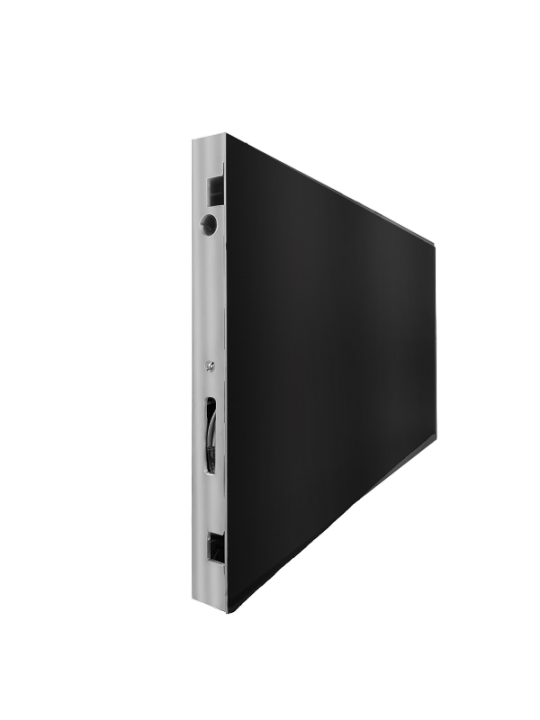
Small spacing LED display splicer technology
With the continuous advancement of technology, small-pitch LED displays have become the first choice in many high-end applications due to their seamless splicing, high definition and excellent display effects. However, to give full play to these advantages requires not only high-quality image processing and exquisite assembly technology of the LED display itself, but also a powerful image splicing processor - that is, a splicer. This article will delve into the technical requirements of small-pitch LED display splicers and their key role in a variety of application scenarios.

Core technical requirements for image stitching processors
Output synchronization: In order to ensure the smoothness and unity of the spliced picture, the splicer must ensure the synchronization of all output signals. This can avoid screen tearing and desynchronization, especially when playing high-speed moving images, synchronization is particularly important. Introducing synchronous control and asynchronous control of LED display to you.
Image processing algorithm: As the pixel pitch of LED displays shrinks and the viewing distance becomes closer, the image processing algorithm must be able to keep the image clear after scaling. This means that the splicer needs to have optimized image processing capabilities to ensure that the edges of the image are smooth, alias-free, and the brightness is uniform. What is a fine-pitch LED display?
Custom output resolution: Since the physical resolution of LED displays may be irregular, the splicer needs to be able to support custom output resolution to accommodate display screens of different sizes and specifications. Provide you with LED display specifications.

Splicing processing technology for small-pitch LED displays
The splicer can output multiple DVI signals to achieve seamless splicing of multiple displays. For very large-scale LED displays, they are usually composed of independent display areas driven by multiple LED controllers. The splicer needs to provide DVI output interfaces that match the number of LED controllers and effectively splice the entire LED screen.
Key technical points include:
Signal output synchronization: Ensure the synchronous output of multiple DVI signals, avoid screen tearing at the splicing point, and ensure the integrity and coherence of the playback content.
Graphics processing algorithm: Use high-end image processing chips or complex FPGA graphics processing algorithms to ensure that the image can still maintain the best display effect after being reduced, and to avoid edge jagged edges and missing pixels. Take you to understand LED chips: technology, application and development.
Non-standard resolution output: The splicer should support non-standard resolution output to adapt to different splicing methods and resource allocation, effectively saving the number of LED controllers and transmission equipment used.

Wide application of small spacing LED displays
Small-pitch LED displays have a wide range of applications, covering many fields such as military exercises, public security, power dispatch, traffic monitoring, energy production, government meetings, radio and television, and public information release. As a new generation of display terminals, small-pitch LED displays are providing high-quality visual experience for key systems in various industries. Provide you with small spacing LED display price and buying guide.
In summary, the splicer for small-pitch LED displays is not only the core of the technology, but also the key to achieving high-quality display effects. By continuously optimizing and upgrading image processing algorithms, synchronization technology and output resolution customization capabilities, the splicer can meet the growing market demand and provide stable and reliable display solutions for various high-end applications. With the continuous advancement of technology, we expect that small-pitch LED displays can exert greater potential in the future and bring users a more shocking visual experience.
Thank you for watching. I hope we can solve your problems. Sostron is a professional LED display manufacturer. https://sostron.com/about We provide all kinds of displays, display leasing and display solutions around the world. If you want to know: Advantages of wireless LED displays. Please click read.
Follow me! Take you to know more about led display knowledge.
Contact us on WhatsApp:https://api.whatsapp.com/send/?phone=8613570218702&text&type=phone_number&app_absent=0
0 notes
Text
Sometimes, when making your own devices on microcontrollers, there is a need to display huge amounts of information on a display and to use a bigger screen for ease of perception. Unfortunately, there are no ready-made and budget-friendly solutions for this task on the market. LCD displays with the ability to connect to a microcontroller are usually tiny and pricy.
But at the same time, there is a wide selection of legacy LCD monitors with a VGA interface. Models with a diagonal of 15 to 19 inches can be purchased in perfect working condition for a very low price, or one can even get one for free. This especially applies to monitors with a 4:3 aspect ratio. In addition, such models are usually quite reliable.
Most older monitors only have a VGA connector for connecting to a computer. Sometimes there is an additional DVI port (on more expensive models). The HDMI connector is more common on modern devices.
Thus, with a probability close to 100%, we'll get just a VGA on an older monitor. In order to display an image on such a monitor, it is enough to work with only five signals: analog R (red), G (green), and B (blue), responsible for the brightness of each color component, as well as digital HS (horizontal sync) and VS (vertical sync), providing synchronization. Analogue signal levels should range from 0 to 0.7 V, where 0 V corresponds to no light at all and 0.7 V to maximum brightness. Digital signals HS and VS are short pulses with a TTL level of negative polarity. The timings of these signals can be found, for example, here: http://tinyvga.com/vga-timing/640x480@60Hz.
Typically, special controllers, or FPGAs, are used to generate video signals, and many FPGA development boards are already equipped with a VGA connector. However, FPGAs are often expensive and require many additional components. I was looking for a simpler and cheaper solution. As a result, the decision was made to use CPLD. CPLDs have fewer available logic gates (LEs) than FPGAs but are less expensive. For example, the MAX II Altera EPM240 development board is sold on Aliexpress: https://www.aliexpress.us/item/3256804686276488.html for only $8.12 (excluding shipping), and the kit even includes a programmer. The chips themselves can be purchased for $1.6–2.1 (for nice knockoffs).
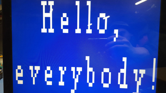
Plain text mode was chosen for implementation because it is easier for a slow microcontroller but at the same time quite informative. Some graphics elements can be implemented using pseudo-graphics symbols, as was often done in the days of DOS. The introduction of a graphics mode would require transferring a large amount of data from the microcontroller and additional efforts to create it, which is not always possible, especially for weak cores.
CPLD has a built-in Flash ROM (User Flash Memory block, UFM), which can be used as a character ROM. However, its capacity is very limited—only 8 kbit, or 1 KB. This amount of storage is only sufficient for characters with a resolution of 5×7 pixels, and only if we discard non-displayable, insignificant, and visually identical characters from the ASCII table. In addition, the use of UFM will require the use of logic gates (LE), of which there are already a few. Despite the attractiveness of this option, I had to abandon it and use an external ROM chip, which can be salvaged from an old motherboard. Choosing a microchip with a supply voltage of 3.3 V will eliminate problems with matching voltage levels for the CPLD. The capacity of such ROMs is quite large: 2, 4, or 8 Mbit, or at least 256 to 1024 KB, which allows one to store a large number of different fonts with a decent resolution of 8x16 pixels.
To store the screen image, you will also need a RAM chip. Let's estimate the approximate size required for this. If we plan on using an 8×16 pixel font on a screen with a resolution of 640×480 pixels, we will end up with 80 characters per line and 30 lines on the screen. Thus, saving the screen image will require 80 × 30 = 2400 bytes. This number is somewhat inconvenient because it is just slightly larger than the nearest power of two, 2048. The memory use in this case is inefficient—only 58%, since the next power of two is 4096. By the way, this is exactly why text mode with 80×25 symbols became popular since there are 5 fewer lines on the screen. In this case, only 2000 bytes of memory are needed, which easily fits into 2 KB.
However, modern memory chips have significant storage sizes, and saving memory is not so critical nowadays. Moreover, one can deliberately choose to waste memory in order to simplify the decryption logic and save CPLD logic elements. Then you will need at least 4096 bytes (2^12, 12 address bits), which can be divided as follows: 5 address bits are allocated to the row address on the screen (30 of 32 will be used) and 7 bits to the column or position address characters in the string (80 out of 128 will be used).
4096 bytes are required only for storing ASCII symbols. The same amount of memory will be taken by the symbol attribute page. Attributes must include character color (3 bits), background color (3 bits), underline, and blinking. So, a memory of at least 8 KB is required.
Of the most affordable options, the best one is static RAM (used as cache memory), also salvaged from old devices or motherboards. It should be noted that this memory can only operate at 5 V. However. If it is a CMOS-type memory, it can take 3.3 V, but this will require timing correction.
So, we got the following diagram:.
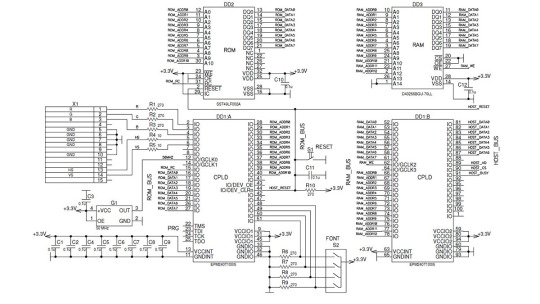
The circuit includes only three microchips and a minimum number of external components. Using the aforementioned Altera EPM240 development board as a base, all you need are ROM chips, RAM chips, and a DSUB header with five resistors. Connecting signals to the CPLD is just an approximation, since almost all of its pins are equivalent (with the exception of Global CLK, one of which requires connecting a signal from a clock generator). When the chip is repeatedly reprogrammed for a new device, almost all of its signals can be reassigned. Currently, the device is assembled on a breadboard and can be left aside.
The device communicates with the microcontroller via a parallel 8-bit interface (in the diagram, signals with the HOST prefix), which is logically almost identical to the widely used display interface on the 1602 and similar controllers. The only difference is the addition of a BUSY signal directed from the device to the microcontroller. Its necessity is due to the fact that access to the RAM chip is provided only during the backward sweep period. The rest of the time, the chip is busy (pun intended) executing CPLD logic. The BUSY signal also acts like an interrupt request (IRQ) function. When it's changed, the controller can automatically start writing to the screen buffer.
Interface description:
DATA[7:0] – eight bits of data, unidirectional port, intended exclusively for writing to the device
CS – chip select; 0 for chip is selected, 1 for chip is not selected. On the positive edge of the CS signal, the data is latched for writing.
AD – address/data, during a write operation: 0 – data is being transferred; 1 – address is being transferred.
BUSY – device busy state; 0 – free; 1 – busy. If the device is busy, the write operation to RAM is ignored. Writing is only possible to the address register.
RESET – device reset. 0 – reset; 1 – work. A hard reset can be used to turn off the screen immediately. When this signal is activated, the image output to the monitor stops. Resetting does not affect the contents of the RAM chip.
Writing data from the microcontroller to RAM is possible only during the backward sweep of the frame scan, when the RAM chip is not occupied by the CPLD logic. This time interval is 1.440 milliseconds. Despite the significant duration of this interval, when using slow microcontrollers, there may not be enough time to completely rewrite the entire memory space. For example, an AVR microcontroller, when operating at a frequency of 11.0592 MHz, is capable of recording only three full-screen lines with all the attributes. If one does not update the attributes (as is usually the case in real-life applications, attributes are written once when the program starts), then six full rows can be written in this time. Perhaps optimizing the code and rewriting it in assembly language can significantly speed up the process of updating data. Otherwise, it may take from 5 cycles (if updating only the data) to 15 cycles (if updating the attributes) to completely rewrite the screen. At 60 fps, it will take 1/12 to 1/4 of a second. Those who have ever worked on IBM PC/XT or IBM PC/AT computers with processor clock speeds around 4 to 12 MHz may notice the experience of refreshing the screen to be familiar.
If you don’t want to wait for the next vertical pulse and want to record all the data at once, you can use the RESET signal. When activated, the internal logic of the CPLD stops and is disconnected from the RAM chip, allowing the microcontroller to directly access the memory. Registers for working with RAM are not affected by the reset signal.
In general, the write operations are as follows: you need to wait until the BUSY signal becomes zero, then put the desired data on the data bus, set the data type (address or data) AD, and set the CS signal first to 0, then to 1. When this signal changes from 0 to 1, the data is stored in memory. During a vertical pulse, the RAM chip is directly connected to the microcontroller's HOST signals, so maintaining the timings during writes becomes the responsibility of the microcontroller. However, since static RAM is a fairly fast device and typically has timings significantly smaller than the maximum speed of an average microcontroller driving its I/O lines, this task is not difficult.
The RAM chip D43256BGU-70LL is connected to the CPLD's output pins, with the lines having a 'RAM' prefix on the diagram. These signals include an 8-bit bidirectional data bus and a 13-bit address bus. Of the control signals, only the WE signal is used. Since there is only one chip on the RAM bus and both buses (address and data) are completely under its control, the OE and CS signals are not used, equal 0, and connected to GND.
The SST49LF002A ROM chip is connected similarly (signals with the 'ROM' prefix), except that the data bus in this case is unidirectional. The OE and WE signals of this IC are also not used and are directly connected to 0 (GND) and 1 (VCC), respectively.
Jumpers are connected to the available CPLD pins to select the current font. Since the ROM chip is large enough, it allows one to store several different fonts, including national alphabets, and switch to them by installing jumpers.
The DSUB VGA port is connected to the CPLD using only 5 resistors. Resistors in the HS and VS circuits are primarily for protection and can be ditched. Resistors in circuits R, G, and B are selected in such a way that, together with the input resistance of the monitor (75 Ohms), they form a voltage divider that reduces the voltage at the monitor input to 0.7 V.
The power leads are shunted with ceramic capacitors, and the clock signal with a frequency of 50 MHz from a crystal is supplied to the GCLK0 pin. These parts were on the breadboard originally.
A resistor, a capacitor, and a button are connected to the RESET signal, forming it. However, if the signal is generated by a microcontroller, these components are redundant.
After creating the main part of the CPLD operating logic, it became clear that the number of logic elements (LEs) used was slightly over half of the available ones. In this regard, the idea arose to complexify the logic and add more features. First of all, the number of colors can be increased to 16 by adding three additional CPLD pins and three resistors. This won't significantly complicate the scheme, but it will add eight more colors. In this case, the RAM page with attributes will have to be completely devoted to color, and another page with attributes will have to be added, increasing the RAM address bus by 1 bit. In the second page of attributes, you can implement font selection, underlining, character and background flickering, and so on.
The new scheme looks similar to the previous one.
As the number of colors increases, the question is: which palette to choose? With only 8 colors, there is no such question; all colors are different combinations of the three primary colors: red, green, and blue (2^3 = 8). When there are more colors, different options are possible. For example, the 16-color EGA palette: https://moddingwiki.shikadi.net/wiki/EGA_Palette:
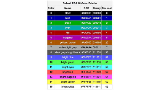
As can be seen from the presented palette, the 4th bit in the color number stands for brightness. However, the halves of the table are not evenly separated by brightness. The first half is set to 2/3 brightness (byte AAH = 170 = 2/3 × 256). In the second half, another 1/3 of brightness is added (byte 55H = 85 = 1/3 × 256), and the colors in this part are called "bright."
Interestingly, color No. 6 (yellow/brown) in this scheme deviates from the expected AAAA00 and is specifically set to AA5500. This was done to replace the unattractive, dirty yellow color with the more appealing brown. This is a known feature of EGA video cards and monitors. Some monitors took this into account, while others did not implement this feature in order to simplify the circuit. Some models added a BROWN ADJ knob so that the user could set the desired shade of that color. That is why the color in the table is indicated as yellow/brown.
Nonlinear separation by brightness level automatically leads to two shades of gray showing up: light gray and dark gray, which are widely used.
In the 16-color VGA palette: https://lospec.com/palette-list/microsoft-vga, the situation is slightly different: the colors are divided exactly in two halves by brightness (80H = 128 = 1/2 × 256):

There is also a noticeable outlier in this palette: light gray (С0С0С0), which should be black, duplicating an existing color. Additionally, this color swapped places with the dark gray color (808080). This was done intentionally to ensure compatibility between the VGA and EGA 16-color palettes, making them almost identical.
In our case, when the R, G, and B signals are generated in hardware using resistors, it is more convenient to use the EGA palette. So, it is necessary to make a software correction only for one color, No. 6. All other colors are generated automatically. Switching to the VGA palette would require not only a program change but also an additional group of resistors to be added to create the light gray color (C0C0C0). The resistors should be picked so that one group provides a brightness level of 1/3, the second is 2/3, and together they provide full brightness. By simple calculations using Ohm's law, we get the following values: 390 Ohms and 750 Ohms.
The signal generation logic for a static image like the one with test color bars is quite simple. However, if it is necessary to generate a dynamic image, the task becomes more complicated. It is necessary to organize a logical interface with RAM and ROM. At the same time, data exchange should occur not just quickly but lightning-fast! Let's first evaluate whether the selected chips can keep up with operating like this.
So, the resolution is 640x480. Pixel output frequency is 25 MHz (the standard specifies 25.175 MHz, but rounding to 25 MHz is acceptable since VGA, like many other analog standards, allows a significant spread of parameters). The frame refresh rate is 60 Hz (actually 59.5 Hz), and the line refresh rate is 31.46875 kHz (actually 31.25 kHz). Thus, the output time of one pixel is 40 ns, and the output time of an 8-bit character is 320 ns. During this time, the ASCII code of the character (one byte), the color code (one byte), and the attributes (one byte) should be read from RAM, and then, using the ASCII code as an address, we should read the bit mask of the character from ROM. Only then will the CPLD logic have all the necessary information to begin imaging.
According to the technical description (datasheet), for the selected D43256BGU-70LL chip, a full read cycle takes 70 ns. Considering the use of the chip at reduced voltage, the read cycle takes longer—let's say, 100 ns. Thus, in 320 ns, we will have enough time to read three bytes from RAM: ASCII code, color code, and character attributes. Great. The situation with ROM is more complicated: the address is written to it in two steps—in rows and columns—and, according to the manual, the read cycle takes 270 ns. Not the highest speed, but within the required 320 ns, even with time to spare.
The problem is that we can't start issuing the ROM address until we know at least the ASCII code, which takes 100 ns. This sums up to 370 ns. What saves us is the fact that each RAM or ROM read cycle individually fits within the allowed interval, and we can simply spend two additional cycles reading data. To add these two loops during data preparation, it is necessary to shift the character display area, creating an additional blanking area 2 characters wide at the beginning of the line and reducing the same area at the end of the line by 2 characters. This is quite simple to do: we simply shift the horizontal blanking pulse by 640 ns (accordingly, the horizontal sync pulse also shifts). From the monitor's point of view, there is no difference.
To better understand when and what to write and read, it is handy to create a timing diagram. At the beginning, all the timings were in my head, but creating a paper diagram and giving it another look allowed me to significantly optimize read cycles and even reduce the number of registers used.
The cycle begins by setting the RAM address of the ASCII character byte on the bus. After 80 ns, the requested byte appears on the RAM data bus, which is instantly used to generate the byte read address from the character generator ROM. At the 100 ns mark, we set the address of the symbol attributes byte to the RAM address bus. At 140 ns (60 ns after setting the address), we latch the first part of the ROM address. After another 60 ns, we set the second part of the address on the ROM address bus. At this point, there should be a byte of data on the RAM data bus with character attributes, where 5 bits correspond to the font and are included in the second part of the ROM address. The remaining 3 bits of data are stored in temporary register 2. After another 60 ns, we latch the second part of the ROM address. Data will appear on the ROM data bus 120 ns after this event, already during the second cycle. To prevent loop intersections, we write this data to temporary register 1 at 80 ns. And finally, at 300 ns, all the prepared data is written to the working registers. The character bitmask from temporary register 1 is copied into the rom_reg register, and the stored attribute bits are applied to the color byte that has been read at that time.
Thus, by the end of the second loop, all the data will be ready for outputting the symbol.
Writing data from the microcontroller to RAM is carried out as follows. We wait until the BUSY signal becomes zero, after which we set the starting addresses in the registers where data will be written. Typically, this is address 0, corresponding to the start of the data page, but a random address can also be chosen if only a few bytes need to be changed. Then we record the data. After each byte is written, the address is automatically incremented. When the edge of the screen is reached (the 80th character in a line), the address of the character position in the line is automatically reset to zero, and the line address is incremented by 1. After the entire page of data is written, the address is automatically adjusted to the attribute page entries and then the color page entries. After writing all three pages, the address is also automatically reset, and the process begins again with writing to the data page. Thus, the start address is set only once, and then only data is written. This saves a few microseconds on address setting and simplifies the code when all data can be transferred in one cycle.
Data format for writing data (AD=0):

The data page stores ASCII character codes.

The attributes page stores symbol attributes. The lower two bits are responsible for the hardware-driven blinking of a character or background, and the third bit is for the underline. The upper 5 bits select the font. Accordingly, you can display characters from different fonts mixed in any combination. 5 digits for selecting the font allow one to store 32 different fonts, which can include any symbols of national alphabets as well as tiles for displaying an image.

The color page contains the character color and the background color. Color can be anything from the 16-color palette.
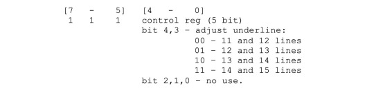
There are three address registers. The choice of which particular one to write to is defined by the most significant bits of the data byte. If the most significant bit [7] is 0, then the position register in the row (column) is written. If it is 1, then the line number register (line) and RAM page number register (ASCII code, attributes, or color) are written. If the three most significant bits are equal to 1, then a special control register is written, bits [4] and [3] of which determine the position of the hardware-generated line when the underscore bit is turned on, and bits [2–0] are reserved for future settings.
Data format for writing address (AD = 1):

A register stores the position in a string.

The register stores the line number and page selection.
If you set an address outside the range of 0-79 for a column and 0-29 for a row, then data will begin to be written to the shadow memory area, which is not displayed on the screen. There is nothing wrong with this; after passing the address 127, the data will again be written to the visible area.
Internal CPLD registers (some):
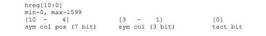
The register contains the current horizontal scan position. It is clocked at a frequency of 50 MHz, which is two times the required 25 MHz, so the least significant bit (tact bit) is not used. Accordingly, bits 1 to 3 indicate the position within the character, and bits 4 to 10 indicate the position of the character in the string. When the value reaches 1600, the register is reset to zero, and the value in the vreg register is increased by 1.
The register contains the current vertical scan position. Clocked from the hreg register. Bits 0 to 3 indicate the line within the character, and bits 4 to 8 indicate the line on the screen. Bit 9 is not used. When the value reaches 525, the register is reset to zero.
The registers contain the current address value for accessing RAM (16 KB in total). The lower 7 bits are the character address in the line (column), then 5 bits are the line address, and 2 bits are the page address (ASCII code, attributes, or color). There are two of these registers: one for internal use by the CPLD logic, and the second is controlled externally by the microcontroller.
The ROM address register is written in two stages. It contains the character string address, the character's ASCII code, and the font address. These addresses are located in such a way that one can flash standard DOS *.fnt font files into the ROM without any additional processing, just one after another. You can combine several fonts into one file for firmware using any file editing program. Just make sure that the fonts have a resolution of 8x16.

Color output register. This register is connected directly to the CPLD pins, supplying the R, G, and B signals to the monitor. The lower 3 bits provide a signal with 2/3 of a brightness level (they must be connected to 390 Ohm resistors); the highest ones provide a signal with a brightness level of 1/3 (they must be connected to 750 Ohm resistors).
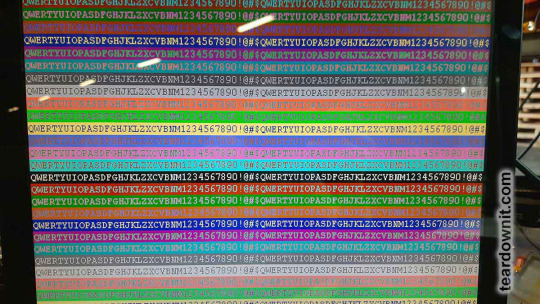
Photos to illustrate:
0 notes
Text
Laboratory 7 – Simple VGA Driver to Display 256 Different Colors
This project is part of the course ‘Digital System Design Lab’. The purpose of this lab is to design a VGA driver to display 256 different colors on a monitor. The color data of each pixel is generated using an 8 bit counter implemented on an FPGA board. Description The VGA driver project generates two timing signals, `vsync` and `hsync`, to synchronize the plotting of vertical and horizontal…

View On WordPress
0 notes
Text
Simple Electronics Projects for Engineering Students
Are you a Final year student? Looking for “Simple electronic projects”? Then I have a Suggestion for you, Takeoff Edu Group provide number of project for Final year Students. Here we furnish a best Ideas and innovative projects for all Kind of Students (like Beginners to Advanced) based on their needs.
As an Engineering Students, You have to work on Simple Electronic projects on your Academic year.
Here are a few Takeoff Edu Group Title of simple electronic projects

Trendy Projects:
Virtex 7 FPGA Implementation of 256 Bit Key AES Algorithm with Key Schedule and Sub Bytes Block Optimization.
A Low-Power Low-Cost Design of Primary Synchronization Signal Detection.
Approximate Belief Propagation Decoder for Polar Codes.
Unequal Error Protection Code Derived from Orthogonal Latin Square Code.
Design and Implementation of a Hybrid Switching Router for the Reconfigurable Network-On-Chip.
Standard Projects
The Mesochronous Dual-Clock FIFO Buffer.
A Double Error Correction Code for 32-bit Data Words with Efficient Decoding.
Security Enhancement of Information using Multi-layered Cryptographic Algorithm.
Fast Mapping and Updating Algorithms for a Binary CAM on FPGA.
Security Enhancement of Information using Multi-layered Cryptographic Algorithm.
LED Blinking Circuit:
Components: LED, Resistor (220 ohms), Breadboard, Jumper wires.
Connect the LED and resistor in series and then connect them to the power source. The LED should blink on and off.
Buzzer Circuit:
Components: Buzzer, Resistor (1k ohm), Transistor (NPN, e.g., 2N3904), Breadboard, Jumper wires.
Connect the buzzer, resistor, and transistor in a circuit. Apply power, and the buzzer should produce sound.
Light-Activated Switch:
Components: LDR (Light Dependent Resistor), Resistor (10k ohms), Transistor (NPN), LED, Breadboard, Jumper wires.
Connect the components such that the LED turns on when light falls on the LDR.
Temperature Sensor with LM35:
Components: LM35 temperature sensor, Resistor (1k ohm), LCD display, Breadboard, Jumper wires.
Connect the LM35 to the LCD display to measure and display the temperature.
Simple Audio Amplifier:
Components: LM386 IC, Capacitor (10uF), Capacitor (0.1uF), Resistor (10k ohms), Speaker, Breadboard, Jumper wires.
Connect the components to create a basic audio amplifier circuit.
The above-mentioned Article are only the example of “Simple electronic projects”?, Here Takeoff Edu Group provide All kind of Academic projects with best project knowledge and support to Student necessities.
Why are you waiting for join and let’s start your Electronic Project today with Takeoff Edu Group.
0 notes
Text
5G ORAN BASE STATION

Faststream has been at the forefront of mobile networking evolution, seamlessly transitioning from 4G to 5G technologies. Our commitment lies in delivering cutting-edge, next-generation experiences and connections for customers and partners. Early investments in key 5G technologies have empowered us to provide highly differentiated offerings in 5G Base Station, Core Network, RAN, Management, and Applications.
5G Ecosystem Overview
5G Revolution
The advent of 5G promises a revolutionary shift in mobile networking, significantly increasing wireless data capacity and unlocking new possibilities for driverless vehicles, smart factories, remote surgery, and more. Establishing a sophisticated ecosystem of hardware, apps, and services is crucial, along with deploying 5G networks in the mmWave frequency, including the 26 GHz pioneer band.
Open RAN in Focus
Investors are keenly interested in the Open RAN instrument. This design promotes interoperability of wireless network hardware/software, breaking free from vendor lock-in. Open RAN fosters innovation by allowing new vendors to contribute use cases, apps, and services, driving competition and potentially reducing costs for mobile operators.
Components of a 5G Network
Macrocell: The Key Component
A 5G macrocell, a vital component of the network, utilizes Multiple-Input, Multiple-Output (MIMO) technology to provide cellular network radio coverage. Positioned on towers, these macrocells, with their MIMO antennas, can link billions of devices while minimizing latency.
Base Station Components
Central Unit (CU)
In a 5G network, the CU consolidates and manages upper-layer protocols across Distributed Units (DUs). Designed for data center deployment, the CU enables cost-effective creation of large capacity networks using FPGAs, Network Synchronization ICs, Ethernet, and Precision Crystal & SAW Oscillators.
Distributed Unit (DU)
Functioning like the typical modem of a 5G Base Station network, the DU is essential for delivering increased capacity and expanded capabilities, such as coordinated multipoint (CoMP). Faststream engineers face challenges in delivering higher capacity at a fraction of the power and cost per bit.
Radio Hardware Unit (RU)
The RU transforms radio signals from and to the antenna into digital signals for packet networks. It manages the digital front end, lower PHY layer, and digital beamforming. Considerations for RU design include size, weight, and power consumption.
Radio Frequency and Massive MIMO
MIMO System
The MIMO system, utilizing "Multiple Input, Multiple Output," enables 5G macrocells to send and receive data through antennas with multiple connections. "Massive MIMO" allows macrocells to connect with an even larger number of users without a significant increase in physical size.
5G MacroCell Range
The range of 5G macrocells can extend kilometers, providing service to major towns. Despite the extensive antenna ports, massive MIMO base station antennas maintain a size comparable to 4G and 3G base station antennas.
5G Software Components and Functionality
To meet the growing data demands of smartphone capabilities, infrastructure design in digital mobile communication systems is evolving. Integrated DDC (Digital Down Converter) and DUC (Digital Up Converter) channels play a crucial role in achieving faster data rates. Leveraging DSPs, FPGAs, and ASICs streamlines design efforts, saving costs and power.
Conclusion
Faststream's commitment to innovation and strategic investments has positioned us at the forefront of the 5G revolution. From advanced network components to embracing open standards, we are dedicated to delivering unparalleled 5G experiences for a connected future.
1 note
·
View note