#Impedance Control PCB
Explore tagged Tumblr posts
Visit Tumblr Blog
Explore Tumblr blogs with no restrictions, modern design and the best experience.
Last Seen Tumblr Blogs


Fun Fact
Tumblr is available in 18 languages.
Text
Understanding Board-to-Board Connectors
In the world of electronic hardware, where space, speed, and signal integrity define performance, board-to-board connectors are critical components that quietly enable innovation. These specialized connectors join printed circuit boards (PCBs) directly without the need for cable assemblies, supporting compact, high-performance electronic designs used in everything from smartphones and laptops to industrial machinery and aerospace systems.Get more news about Board-to-board Connector,you can vist our website!
What Are Board-to-Board Connectors? Board-to-board connectors are designed to provide reliable electrical and mechanical connections between two or more PCBs within a device. Unlike wire-to-board or cable-based systems, these connectors allow signal and power transmission through directly mated interfaces, which helps reduce bulk and improve data integrity. They are essential for stackable or modular designs and are particularly favored in applications where internal space is limited.
Types and Configurations These connectors come in several configurations depending on the orientation and spacing needs:
Parallel (Mezzanine) Connectors: Used when two boards are stacked vertically. These are common in compact electronic devices and offer high-density signal transmission.
Coplanar Connectors: For side-by-side board connections, maintaining the same plane and allowing broader layout designs.
Right-Angle Connectors: Used when a 90-degree connection is required between boards, useful in folded or L-shaped PCB assemblies.
Pitch (the spacing between pins), stack height, current rating, and number of contacts are customizable depending on application requirements. High-speed data connectors often require shielding and controlled impedance to prevent signal loss and crosstalk.
Key Features and Advantages Modern board-to-board connectors are engineered for precision and durability. Key features include:
Miniaturization: Compact design supports smaller electronic devices.
High-Density Pin Configuration: Enables transmission of large volumes of data and signals.
Durability and Reliability: Designed for multiple mating cycles and resistance to shock and vibration.
High-Speed Signal Transmission: Particularly in designs requiring signal integrity for data communication or computing.
Manufacturers also offer versions with alignment guides, locking mechanisms, and surface-mount or through-hole mounting options, ensuring seamless assembly even in automated production lines.
Applications Across Industries Because of their versatility and performance, board-to-board connectors are used in a wide range of industries:
Consumer Electronics: Smartphones, tablets, laptops, and wearables.
Industrial Automation: PLCs, sensors, and motor controllers.
Medical Devices: Diagnostic imaging machines, patient monitors, and handheld tools.
Automotive: Advanced Driver Assistance Systems (ADAS), infotainment, and battery management systems in EVs.
Aerospace and Defense: Flight systems, navigation equipment, and satellite electronics.
As electronics become smarter and more integrated, the demand for connectors that balance power, data throughput, and mechanical integrity has never been higher.
Innovation and Market Outlook The global board-to-board connector market is expected to grow steadily, driven by trends such as miniaturization, 5G deployment, IoT integration, and automation. Emerging materials and manufacturing techniques—like laser welding and micro molding—are allowing for even smaller, faster, and more durable connectors.
Asian countries, particularly China, South Korea, and Taiwan, dominate production, but leading global manufacturers like Samtec, TE Connectivity, and Hirose Electric continue to drive innovation with proprietary designs optimized for high-speed and harsh-environment applications.
Conclusion Board-to-board connectors might not be visible to end users, but they are indispensable to modern technology. As we continue to demand more from our devices—in performance, portability, and connectivity—these small yet powerful components ensure that everything works as one cohesive system. Their evolution mirrors our own digital advancement: quietly essential, endlessly adaptable, and critical to progress.
0 notes
Text
Navigating the Future of Electronics with Rigid-Flex and Taconic PCB Manufacturers
Today’s Printed Circuit Boards (PCBs) are much more flexible and advanced than the first rigid versions. Compact devices with great capabilities and multiple features have earned popularity in the electronics industry, leading to the rise of Rigid-Flex PCBs and Taconic PCBs. The use of these technologies enables unique designs, improves how long the device works, and maintains good electricity flow. Rigid-flex PCB Manufacturers can move and also keep their form, similar to how rigid boards function. They particularly shine in high-speed or RF and microwave applications. Dependable and effective products rely greatly on what electronics do.
Rigid-Flex PCBs: Hybrid Structure with High Functionality
Rigid-Flex PCBs take attributes from both stiff and flexible PCBs and merge them into one board. As a result, rigid and flexible boards no longer need connectors and cables, letting us make assemblies that are lighter and more space-saving. You can find these boards in smartphones, medical devices used on patients, military systems and aerospace devices. They are suited for use in places that require resistance to vibration and bending due to machines. In manufacturing, various layers are made and bonded together using very accurate methods. Therefore, it is only experienced manufacturing companies that can keep products of constant quality and performance.
Key Advantages of Rigid-Flex PCB Manufacturers
Important benefits of using well-known Rigid-flex PCB Manufacturers are their excellent design aid and advanced methodologies. They depend on laser direct imaging for precise work and optical inspection that finds problems in the early stage. Tests using temperature fluctuation and electrical overload guarantee that the product will function in any extreme condition. Manufacturers typically boost efficiency by assisting with design changes that lower the number of components and simplify assembly. In addition, they guarantee that flexible circuit boards meet all IPC standards for quality. Because they are involved in developing products and moving them into mass production, they help make the process more efficient.
Taconic PCBs: High-Frequency Performance Excellence
Taconic PCB Manufacturers are produced from proprietary PTFE-based laminates designed by Taconic with low dielectric loss and thermal stability. These boards are the preferred option for RF, microwave, and high-speed digital designs. They are most prevalent in satellite communications, radar systems, 5G base stations, and aerospace communication modules. Taconic laminates have low signal attenuation and superior dimensional stability. They exhibit moisture resistance as well as heat tolerance, which makes them dependable in extreme working environments. Production using these laminates demands proficiency in drilling, plating, and multilayer bonding because of their special properties.
What to Expect from a Taconic PCB Manufacturers
The best Taconic PCB Manufacturers must possess extensive experience in working with high-frequency laminate material. It involves strict impedance control, surface preparation, and low-loss transmission line engineering. Cleanroom facilities, specially designed PTFE-compatible equipment, and precise lamination procedures are necessary for high-quality output. The producers may perform RF testing and thermal profiling to ensure circuit integrity. They also guide customers on stack-up selection as well as PCB layout according to end-use frequency requirements. By maintaining compliance with IPC and MIL-spec specifications, these companies ensure the critical applications' performance and safety.
Comparing Rigid-Flex and Taconic PCBs
Although both are sophisticated PCBs, Rigid-Flex and Taconic PCBs are for different technical applications. Rigid-Flex is prized for mechanical flexibility, whereas Taconic leads for signal transmission at high speeds. Rigid-Flex boards simplify systems and minimize space utilization in cramped enclosures, while Taconic boards maintain signal purity in communication networks. The components and manufacturing methods are quite different, as are the final-use applications. The two are chosen based on physical space, frequency range, and exposure to the environment. Designers will often talk to both varieties of manufacturers to match their circuit requirements with the appropriate solution.
Conclusion
As innovation speeds up in electronics, the need for Rigid-flex PCB Manufacturers and Taconic PCBs keeps increasing. Such technologies facilitate the development of lighter, faster, and more efficient devices across industries. With increasingly sophisticated design challenges, collaborating with an experienced manufacturer is crucial. BS Interconn Hong Kong Co., LIMITED differentiates itself by providing quality-oriented, customer-centric PCB manufacturing services. Whether you're creating a next-generation medical wearable or a state-of-the-art RF device, selecting a reliable Rigid-Flex or Taconic PCB producer guarantees that your product will outperform and outlast the competition.
#Rigid-flex PCB Manufacturers#Taconic PCB Manufacturers#flexible circuit boards#high-frequency PCB#RF PCB solutions#microwave PCBs#PTFE laminates#hybrid PCB design#aerospace PCB#medical device PCBs#5G PCB manufacturer#signal integrity PCB#low dielectric PCB#high-speed PCB#multilayer PCB assembly#IPC compliant PCBs#MIL-spec PCBs#advanced PCB manufacturing#Taconic laminate PCB#Rigid-Flex technology
1 note
·
View note
Text
How to Design Efficient and Reliable Rigid-Flex Circuit Boards?
Rigid-Flex Circuit Boards combine the best highlights of rigid and flexible PCBs into a single bound together structure, advertising creators effective focal points for complex and space-constrained applications. These hybrid Boards are composed of rigid layers that give mechanical soundness and flexible areas that permit energetic development or collapsing. To accomplish both proficiency and unwavering quality in rigid-flex circuit board plan, engineers must take after a set of best hones that consider mechanical, electrical, and fabricating aspects.
Understand the Application Requirements
Before starting the format, it's basic to get it the particular needs of the application. Rigid Flex Circuit Boards are frequently utilized in aviation, military, therapeutic gadgets, and progressed shopper hardware — all situations that request tall unwavering quality. Architects must consider space limitations, mechanical stretch, electrical execution, and natural introduction to guarantee that the board meets execution and solidness expectations.
Use Legitimate Layer Stack-Up Planning
A well-structured layer stack-up is key to accomplishing flag keenness and mechanical quality. In rigid-flex circuit Boards, the move between the unbending and flexible areas must be smooth and free of push concentration. Legitimate stack-up arranging incorporates deciding the number of layers, copper weight, dielectric materials, and the twist span of flexible locales. Dodging as well numerous layers in the flex range makes a difference avoid delamination and splitting over time.

Maintain Controlled Twist Areas
One of the most common focuses of disappointment in rigid-flex plans is the twist zone. To guarantee long-term unwavering quality, the twist span ought to be at slightest 10 times the thickness of the flex fabric. Twists ought to never happen at the interface between unbending and flexible segments. Moreover, dodge putting vias, cushions, or sharp points in the twist region to decrease mechanical stretch. Utilize bended follows and stunned vias to upgrade adaptability and decrease the hazard of cracking.
Optimize Follow Routing
Efficient directing is fundamental for flag keenness and control dissemination. In rigid-flex circuit Boards, follows ought to be directed opposite to the twist pivot in flexible areas. Parallel follows in a twist range are more likely to break over time. Keep up steady follow widths and dividing, and maintain a strategic distance from 90-degree points in steering, as they can cause flag reflections and push focuses. Controlled impedance plan is moreover imperative for high-speed flag transmission.
Design for Manufacturability (DFM)
Working closely with your PCB manufacturer amid the plan stage can avoid expensive modifications. Utilize standard materials and take after industry rules like IPC-2223 for rigid-flex board plan. Indicate clear mechanical diagrams, resistances, and stack-up subtle elements in the manufacture drawings. Too, incorporate fiducials and test focuses to help in get together and review processes.
Include Intensive Testing and Validation
To guarantee the long-term unwavering quality of rigid-flex circuit Boards, intensive testing is basic. This may incorporate warm cycling, vibration tests, and electrical testing beneath stack. Early approval makes a difference capture plan blemishes and guarantees the board can perform in real-world conditions.
Conclusion
Designing effective and dependable rigid-flex circuit Boards requires a mindful approach that equalizations electrical execution with mechanical judgment. By carefully arranging the layer stack-up, overseeing twist ranges, optimizing follow steering, and centring on manufacturability, engineers can make progressed gadgets that are both compact and tough. With legitimate testing and adherence to plan benchmarks, rigid-flex Boards gotten to be a trusted arrangement for today’s most requesting electronic applications.
0 notes
Text
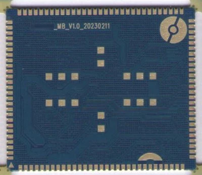
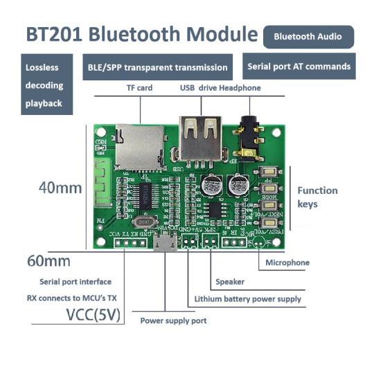
KT1025A Dual-Mode Bluetooth Audio Chip Layout Description and Design Precautions
1.Brief Overview
1. First, please refer to the provided BT201 test DEMO module as the standard.
2. If using the chip independently without testing the BT201 module and directly proceeding to layout, background noise is highly likely if experience is limited. Therefore, always compare with the manufacturer’s test board first.
3. The BT201 solution does not include FM functionality. Please note this. The FM circuit should be left floating without hesitation.
2.Precautions
1. Background noise or interference is common in Bluetooth audio products. Do not be careless during layout.
2. If you have not worked on audio products before, study online resources thoroughly. Assuming things casually will naturally lead to noise issues.
3. The core principle is to separate analog ground and digital ground. If unclear, consult an experienced engineer.
4. Ensure a clean power supply. Use an LDO whenever possible instead of a DC-DC converter.
5. Bluetooth operates at high-frequency RF and radiates energy, so some background noise is inevitable but can be minimized. With good design, noise is imperceptible to the human ear, though it may be measurable with instruments.
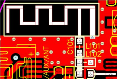
3.Antenna Description
1. For antenna and component packaging, directly refer to the PCB files of the DEMO module, available in the document library.
2. The Bluetooth antenna has no special requirements. Follow the provided package and reference instructions.
3. The Bluetooth antenna does not require impedance matching, and standard copper thickness is sufficient. Don't over complicate it—Bluetooth has a low entry barrier.
4.Power Supply Description
(1)The BT201 test board has minimal background noise, barely noticeable to the human ear.
(2)You can try powering it with a phone charger, which should not produce significant noise.
(3)Battery power is ideal as it provides pure DC and is very clean. However, consider the battery's load capacity.
(4)USB output from a desktop computer may produce significant ripple, leading to background noise. Avoid using it.
(5)If the board includes a DC-DC converter, it may cause noise. The optimal power supply is an LDO, such as a 7805.
(6)The BT201 module can drive a maximum speaker of 4 ohms, 3W with a 5V supply.
(7)When driving speakers, ensure sufficient current with a stable power supply. Insufficient current can cause speaker distortion, buzzing, etc.
(8)If possible, purchase various amplifier modules online for comparison testing. We sell Bluetooth chips, but amplifier-related noise, distortion, or other issues are extended topics that are complex and cannot be explained briefly.
5.How to check if the board has background noise?
(1)Use a clean power supply, ideally a battery, and disconnect all front-end power circuits.
(2)Connect the chip's headphone output and listen for noise. If none, check the rear-stage amplifier circuit.
(3)If USB playback has no noise but Bluetooth does, this does not necessarily indicate a problem.
(4)Use headphones to check for noise. If none, the issue lies in the amplifier section, so inspect it.
(5)If noise is present with headphones, disconnect the rear-stage amplifier and inspect the Bluetooth chip's peripheral circuits. Determine whether noise occurs during Bluetooth or MP3 playback. For Bluetooth noise, check if capacitors around the main controller are properly soldered and if they are too close to the Bluetooth module. Refer to other instructions for troubleshooting.
(6)For noise testing, avoid using a computer's USB or a charger's USB. Use a clean power supply with strong load capacity, ideally tested at 5V, not 3.7V.
6.Methods to Reduce Bluetooth Background Noise
(1)Keep the Bluetooth antenna and Bluetooth module as far as possible from analog circuits.
(2)The chip's analog ground must be connected to the power ground at the input.
(3)Check capacitors around the chip for issues such as short circuits or poor soldering.
(4)Add multiple vias to the GND of the Bluetooth section.
7.Selection and index requirements of crystal oscillators
(1)Bluetooth has high frequency offset requirements, so the crystal oscillator's quality is critical for performance. During selection, ensure consistency and stability, with a frequency deviation of ≤±10ppm and a recommended load capacitance (CL) of 12pF.
Note: Crystal-to-ground capacitors C102 = C103 = 2*CL – (4pF~6pF), where CL is the crystal's load capacitance.
(2)For designs with no size constraints, use the crystal specified in our DEMO, which is cost-effective and high-performing.
(3)For size-constrained designs, use a 24M-3225 crystal, which is slightly more expensive but performs well.
Recommendation: Use our provided crystal, which is more cost-effective and quality-assured compared to random purchases.
8.Simple PCB Layout Precautions
(1)The input voltage to LDO_IN (Pin 18 of the chip) must not exceed +5.5V.
(2)The chip must strictly separate digital GND and analog AGND (refer to the provided BT201 PCB).
(3)During PCB routing, digital GND and analog AGND must be routed separately and connected only at the battery input. If the design includes a pre-amplifier ground, connect AGND to it.
(4)All decoupling capacitors on the main controller must be placed as close as possible to the chip pins, with short ground return paths.
(5)Prioritize the placement of the Bluetooth antenna. The RF antenna must be near the board edge (or in an open area if structural constraints apply). The antenna matching circuit must be close to the RF pin, with short routing. The antenna's ground plane should follow the yellow outline in the antenna package, and the space on both sides should be as wide as possible, as shown in the diagram avove.
(6)The 24M crystal must be placed close to the chip's clock pins (BTOSCO and BTOSCI). Its routing must be shielded with a ground plane, kept away from interference sources, and not routed parallel to other data lines.
(7)Audio signal lines (DACL, DACR, AUXL, AUXR, MIC, etc.) must be routed away from digital signals (LCD/LED signals, USB, SD, etc.).
#bluetooth#audiochip#bluetoothchip#voicechip#ble#spp#electronic#coding#embeddeddevelopment#devlog#aiot
0 notes
Text
What Sets Apart a Great Electronics Design Engineer and a Top-Tier PCB Designer
Developing cutting-edge products requires more than just a basic understanding of electronics—it demands specialized expertise at multiple levels of the design process. While the roles of an electronics design engineer and a PCB designer often overlap, each discipline has its own set of core skills, priorities, and best practices. Understanding these differences can help companies build stronger teams and ensure both functionality and manufacturability from concept to production.
1: Foundations: Concept vs. Layout
Electronics Design Engineer
System-level thinking: Architects circuits that meet performance, power, and cost targets.
Component selection: An electronics design engineer chooses processors, sensors, power supplies, and other parts based on specifications and availability.
Simulation and validation: Uses SPICE, MATLAB, or custom scripts to verify that circuits behave as intended under various conditions.
PCB Designer
Physical realization: Translates schematic diagrams into board layouts, deciding component placement, routing, and layer stacks.
Signal integrity: Manages trace lengths, impedance control, and differential pairs to prevent timing mismatches and noise.
Thermal management: Integrates heat sinks, copper pours, and thermal vias to maintain reliable operating temperatures.

2: Technical Skills: Breadth vs. Depth
Breadth of Knowledge (Engineer)
A great electronics engineer understands analog and digital domains, power management, RF techniques, and often systems integration. Their toolkit includes:
Circuit simulation tools (e.g., Cadence, LTspice)
Firmware debugging (e.g., JTAG, SWD)
Test equipment (oscilloscopes, spectrum analyzers)
Depth of Expertise (PCB Designer)
A top-tier PCB designer goes deep into board stack-up design, advanced routing strategies, and material characteristics:
PCB CAD software mastery (e.g., Altium Designer, Mentor Xpedition)
High-speed design considerations (e.g., controlled impedance, crosstalk analysis)
3: Collaboration and Workflow
Communication Styles
Electronics engineers often work in cross-functional teams—mechanical, software, and compliance—to validate overall design requirements. Their deliverables include schematics, block diagrams, and simulation reports.
PCB designers interact heavily with manufacturing partners. They must document fabrication drawings, assembly notes, and BOM details clearly to avoid production delays.
By recognizing the strengths each role brings—and fostering close collaboration between them—teams can bring innovative, reliable products to market faster and more efficiently.
Source: https://extrondesignservice.blogspot.com/2025/05/what-sets-apart-great-electronics.html
0 notes
Text
PCB Design Driven by Precision, Practicality and Performance

At Arrival Electronics Limited, we understand that PCB design isn’t just a step in product development—it’s the foundation that supports every component, signal path, and functionality. Whether you're developing a next-generation medical device, a robust industrial control unit, or a compact consumer electronic product, our role is to ensure your ideas are backed by dependable, efficient, and expertly engineered printed circuit boards.
With decades of hands-on experience in electronics, our team has worked with companies across multiple industries, helping bring projects to life—from concept through to production.
In this article, we’ll share what makes a strong design, the practical elements that often go unnoticed, and how our services help keep your project moving forward from the drawing board to delivery.
Why PCB Design Matters
Designing the right board isn't just about connecting components—it's about ensuring the entire electrical system performs reliably, consistently, and within its intended environment. A well-thought-out layout contributes to:
Product longevity and durability
Efficient power consumption
Signal integrity and reduced noise
Thermal control and mechanical stability
Overlooking critical details during this stage can lead to performance issues, unnecessary rework, or even total product failure. We take every aspect seriously to help our clients avoid costly missteps and stay on track.
What Makes a Solid Design?
Over the years, we’ve found that strong board design depends on more than just software skills or technical knowledge. It’s about having the awareness to balance practical considerations with real-world requirements. Here’s what we focus on in every project:
1. Clear Design Objectives
Before a single trace is laid out, we work closely with you to understand the end-use of the product. Is it intended for a high-vibration environment? Will it operate at high frequency? These questions shape everything from component selection to board layout.
2. Efficient Layout and Routing
We pay close attention to the physical layout, making sure component placement allows for clean, short signal paths and minimal electromagnetic interference. Where needed, we apply differential pair routing, impedance control, and strategic layer stacking.
3. Manufacturability
A design that’s difficult to produce can quickly eat into budgets and timelines. We align our designs with your manufacturing capabilities—choosing standard sizes, spacing, and materials that avoid bottlenecks in production.
4. Thermal Management
Heat can quietly cause long-term damage. We integrate copper pours, thermal vias, and heat sinks when necessary, ensuring temperature-sensitive components stay within safe operating ranges.
5. Design for Testability
We keep diagnostics in mind from the outset. Well-placed test points and clearly labelled nets allow engineers to easily validate performance and troubleshoot issues during development.
Our Approach
What sets us apart is the level of care and accountability we bring to each project. We don’t treat board design as a one-size-fits-all task. Instead, we tailor our process to match your product’s specific technical and commercial requirements.
Collaborative from the Start
We believe good design starts with good communication. Our team begins by understanding your specifications, timelines, and constraints. If needed, we assist with component selection and design reviews, helping guide decisions that support project success long-term.
In-House Expertise
Our engineers bring decades of collective experience across RF design, digital and analogue electronics, signal integrity, and power distribution. This depth of expertise means we’re equipped to handle both complex multilayer PCBs and simpler single-sided designs with the same level of detail and reliability.
Detailed Documentation
We provide comprehensive documentation for every design, including Gerber files, BOMs, assembly drawings, and test documentation. Everything is clearly structured, so your production team or manufacturer has what they need to get started without delay.
Supporting Every Stage of Development
We understand how interconnected the design process is with the rest of the product lifecycle. That’s why our support doesn’t end once the board layout is finished.
Prototyping
We help bridge the gap between design and validation by assisting with prototype builds. If changes are needed, we provide quick iterations without compromising design integrity.
Compliance
Many products need to meet specific regulatory standards. Our knowledge of EMC, safety, and industry certifications helps keep your project aligned with compliance from the ground up.
Component Availability
Supply chain challenges can affect even the most carefully engineered layouts. We actively review component availability early in the process and suggest practical alternatives when necessary. This helps keep your project on schedule and reduces the risk of unexpected delays.
A Closer Look at Our Capabilities
Here’s a snapshot of the types of board layout work we handle:
Single-sided and double-sided configurations
Multilayer builds (up to 24 layers)
High-speed digital and analog signal routing
RF and microwave applications
Flexible and rigid-flex formats
Power distribution and regulation paths
Projects with tight impedance and signal integrity demands
All layouts are created using industry-standard tools, including Altium Designer and Cadence Allegro, ensuring smooth integration with your existing workflows.
Industries We Serve
One of the strengths of our team is our versatility. We’ve worked with clients across sectors including:
Medical Technology: Supporting devices that require extreme reliability and precise electrical behavior.
Industrial Automation: Creating robust PCBs for use in high-temperature, high-vibration environments.
Consumer Electronics: Helping bring compact and functional designs to market faster.
Automotive: Designing for safety, efficiency, and long-term performance in vehicle systems.
Telecommunications: Handling high-frequency signal requirements and tight timing constraints.
No matter the application, we bring the same level of care and engineering discipline to every project.
Focused on Accuracy
Every layout we deliver goes through rigorous design rule checks (DRC), electrical rule checks (ERC), and internal peer reviews. We follow industry best practices and adapt our quality assurance process to meet the specific standards of your sector.
We’ve earned the trust of clients across the UK by consistently delivering high-quality work with a personal touch. Our focus is on making your project a success—not just through technical execution, but through reliability, responsiveness, and genuine collaboration.
Common Challenges We Help Solve
If you’ve experienced any of the following issues, we’re here to help:
Designs that aren’t manufacturable without rework
Unstable prototypes or unexpected signal behaviour
Thermal problems during test or usage
Poor EMI performance or compliance failures
Designs delayed by long lead-time components
The Edge of Partnering With Us
There are many design services out there. What makes us different is the way we treat our clients and the projects they entrust to us. When you work with us, you get more than a technical service—you gain a partner who’s committed to your success.
We listen. Your needs guide every design decision we make.
We respond quickly. Tight timelines don’t faze us—we’re used to working in dynamic environments.
We follow through. From first sketch to final sign-off, we’re with you every step of the way.
Whether you’re a start-up developing your first prototype or an established manufacturer needing dependable support for your next product line, we bring the right mix of experience, care, and clarity to help you move forward.
Let’s Begin Your Project
IIf you're looking for dependable design services with a team that understands the real-world pressures of product development, we’re here for you at Arrival Electronics Limited. Our process is built around clear communication, careful planning, and engineering you can trust, including expert PCBA services to ensure every component is perfectly integrated.
We’re more than just a distributor—we’re your engineering partner. From bespoke solutions to component sourcing and full system support, we’re here to help turn your vision into reality.
For more about our services or to start a conversation, visit arrivalelectronics.co.uk.
0 notes
Text
Not Just a Netlist: Why True PCB Design Starts After the Schematic
What if your schematic—meticulously drawn and logically flawless—is only the beginning of the real design? Too often, PCB design is mistaken as a process that simply converts schematics into copper. In reality, the layout stage introduces new dimensions: physics, geometry, manufacturability, and risk. This is where engineering becomes an applied art. In this article, we’ll explore how true PCB design unfolds after the schematic is done, and how that process defines the actual success of your board. Let’s sharpen our approach to what PCB design really means.

Schematic Isn’t the Whole Truth
The schematic defines logical connections, but it ignores spatial context. In other words, while it tells you what connects to what, it doesn’t account for how those connections affect each other in a physical medium. Real-world considerations like parasitics, inductance, return paths, and trace geometry are completely absent.
Once you leave the schematic stage, the board begins to behave like a complex, analog ecosystem—even if the design is fully digital. Voltage drops across planes, thermal coupling between components, and interference between signals can radically alter how a "correct" schematic performs in reality.
Component Placement Defines Everything
Component layout is the first—and arguably the most crucial—step in post-schematic design. It influences routing complexity, power distribution, thermal paths, and even EMI behavior.
Flow matters: Think about signal directionality and data flow. Position elements to mirror functional grouping and logic sequence.
Thermal zones: High-power devices should have enough spacing and copper pour for heat to dissipate. Placement directly affects cooling options.
Test point accessibility: Consider debugging early. Hidden or unserviceable components create issues down the line.
Mechanical limitations: Mounting holes, connectors, and enclosures will limit placement, so they should be locked in early.
Poor placement leads to compromised routing and potential signal problems, even if the schematic is flawless.
Routing Is Electrical Engineering in Disguise
After placement, routing turns your conceptual circuit into a real-world one. This step isn't just about making connections—it's about how current and signals travel across a physical medium.
1. Controlled impedance isn’t optional anymore
High-speed signals demand matched impedances and consistent routing geometries. This includes trace width, spacing, and via handling.
2. Return paths matter as much as forward traces
Ignoring return current paths results in ground loops and EMI issues. Careful ground plane design is essential to maintain integrity.
3. Length matching isn’t only for differential pairs
Signals that need to arrive in sync—like address lines on a memory bus—should be length-tuned, even if they’re not differential.
4. Via strategy impacts signal quality
Each via adds inductance. Excessive layer changes can distort high-speed signals, so minimize vertical transitions where possible.
Power Distribution is a Design Discipline
Most schematics show power as a single net label—like 3.3V or GND—but once you start routing, you realize it’s a complex subsystem of its own.
Decoupling placement and quantity: Bulk caps don’t replace local ones. Proper distribution avoids ripple and maintains rail stability.
Plane shape and integrity: Fragmented power planes introduce voltage drop and inductive noise. Solid pours reduce impedance paths.
Thermal coupling: Power distribution should also help manage heat. High-current paths need adequate copper width and thickness.
Design for Manufacturability Isn’t Optional
Many new designers focus on circuit behavior and forget that PCBs are physical products. If the board can’t be reliably manufactured, even the best design fails.
Clearance compliance: Make sure all spacing respects your fabricator’s minimums.
Via-in-pad issues: Unless using filled or capped vias, avoid placing them in pads—it causes solder voids and manufacturing defects.
Panelization awareness: Understand how your board fits into a panel. Odd shapes or edge components can complicate the process.
Silkscreen readability: Overlapping silkscreen on pads or vias can mislead assembly technicians or obscure information.
Thermal Behavior is Invisible Until It’s Not
A board can function perfectly during a bench test, yet fail in the field due to poor heat handling. That’s a design issue—not a system issue.
Use thermal reliefs only where necessary. Too many reduce copper connectivity, affecting current-carrying capacity.
Don’t just rely on heatsinks. Spread heat using planes, vias, and strategic copper pours.
Hot spots often occur near voltage regulators, processors, and RF sections. Early simulations help avoid surprises.
Design Rules are Not a Safety Net—They’re a Language
DRCs (Design Rule Checks) and constraints shouldn’t be used to fix problems—they should guide design. Experienced engineers use constraints like communication tools with the layout.
Customize rules for each layer and net class.
Treat DRCs as dynamic guards, not static thresholds.
Regularly update them during schematic and placement to reflect real-world insights.
Post-Layout Verification Isn’t Just Simulation
Simulation tools are essential, but so is human verification. Carefully examine:
Critical trace lengths
Power integrity
Thermal modeling
EMI hotspots
Layer stack correctness
These checks often uncover issues that no schematic can show—like loop areas, discontinuities, or parasitic resonances.
Conclusion
True PCB design happens where logic meets physics. The schematic is only the blueprint—real design begins when space, current, and heat start interacting. Every trace, via, and pad you place tells a story far beyond simple connectivity. Think beyond the schematic, because that’s where the actual engineering starts.
0 notes
Text
Surface Finishes for Multilayer PCBs and Their Impact
Multilayer PCBs are essential in modern electronic systems where high-density routing, signal integrity, and reliability are critical. While inner layers are encapsulated during lamination, the outer layers of a multilayer PCB are exposed for component assembly — making surface finish a key factor in performance and long-term reliability.
Surface finish not only protects the exposed copper but also directly influences soldering quality, component compatibility, and board lifespan, especially in complex multilayer designs.
Why Surface Finish Is Critical in Multilayer PCBs
In a multilayer PCB, especially those with 6, 8, or more layers, outer-layer copper traces and pads are often extremely dense and designed for fine-pitch SMT components such as BGAs, QFNs, or high-pin-count connectors.
A good surface finish must:
Ensure consistent solderability across dense pad arrays
Maintain flatness to support reliable assembly of micro-components
Provide oxidation protection during storage and processing
Be compatible with lead-free reflow profiles
Handle multiple reflow cycles without degradation
Multilayer PCBs often undergo more complex assembly and higher thermal stress, so the surface finish must meet higher standards than simple single- or double-layer boards.
Common Surface Finishes for Multilayer PCBs
1. ENIG (Electroless Nickel Immersion Gold)
The most popular surface finish for multilayer boards, especially in high-density and high-reliability applications.
Provides excellent flatness for fine-pitch components (e.g. BGAs)
Stable during multiple reflow cycles
Compatible with high-speed signals due to smooth surface
Long shelf life, ideal for staged assembly
Slightly higher cost but justified by performance
Widely used in servers, telecom equipment, and aerospace PCBs.
2. OSP (Organic Solderability Preservative)
Preferred for cost-sensitive multilayer boards with fine-pitch components.
Flat surface suitable for automated SMT
Environmentally friendly and lead-free
Lower cost than ENIG
Limited shelf life, requires controlled handling
Not ideal for boards requiring multiple assembly cycles
Often used in consumer electronics and automotive applications.
3. Immersion Silver
Used for multilayer boards requiring high signal integrity or RF performance.
Low surface roughness ensures good impedance control
Suitable for high-frequency multilayer PCBs
Sensitive to tarnishing and handling
Better electrical performance than ENIG in certain designs
Good choice for communication equipment and high-speed digital boards.
4. Lead-Free HASL
Sometimes used in low-cost multilayer boards, but not recommended for very dense designs.
Cost-effective, robust finish
Less flat surface can cause soldering issues on fine-pitch pads
May lead to solder bridging in dense layouts
Acceptable for through-hole or mixed technology boards
Usually applied to industrial control or power-related multilayer PCBs.
Surface Finish Considerations in Multilayer PCB Design
When choosing a surface finish for multilayer PCBs, consider:
Assembly method (SMT vs through-hole, single vs multiple reflows)
Pad density and component type (especially fine-pitch packages)
Signal performance needs (RF, impedance control, etc.)
Environmental factors (RoHS, storage conditions)
Budget vs reliability trade-offs
In many high-reliability or mission-critical multilayer designs, ENIG or Immersion Silver is preferred despite higher cost, due to their consistent performance.
Final Thoughts
The outer layers of a multilayer PCB may seem like a small part of a complex system, but the choice of surface finish can make or break the final product. Whether it's ensuring reliable solder joints for 0.4 mm pitch BGAs, withstanding multiple reflow cycles, or maintaining performance in high-frequency circuits — the right surface finish is critical.
Understanding the relationship between board complexity, material stack-up, and surface treatment is essential for delivering a reliable, high-performance multilayer PCB.

0 notes
Text
ASC: The Ultimate Destination for High-Performance Digital PCB and PCB Digital Solutions
In the digital age, the backbone of every advanced electronic device is a reliable and efficient digital PCB. At American Standard Circuits (ASC), we specialize in delivering world-class PCB digital solutions that cater to the needs of innovators across a spectrum of industries. From aerospace and automotive to medical, telecommunications, and green energy, ASC’s commitment to quality, speed, and technical expertise makes us the preferred partner for digital PCB manufacturing and design.

Unmatched Expertise in Digital PCB Manufacturing
ASC’s reputation as a leader in digital PCB manufacturing is built on decades of experience, state-of-the-art facilities, and a relentless pursuit of innovation. We offer a comprehensive range of PCB digital services, from the simplest single-sided boards to intricate multilayer and HDI (high-density interconnect) designs. Our advanced capabilities allow us to support even the most complex digital PCB requirements, ensuring your products are equipped for maximum performance and reliability.
Our digital PCB manufacturing capabilities include:
Multilayer and HDI digital PCB fabrication: Up to 40+ layers for sophisticated electronic systems.
Controlled impedance and high-speed signal management: Critical for data-intensive and high-frequency digital applications.
Blind, buried, and microvias: Enabling compact, space-saving PCB digital layouts.
Conductive and non-conductive via filling: Supporting advanced circuit design and reliability.
Edge plating, castellations, and custom finishes: For specialized connectivity and enhanced durability.
Lead-free and RoHS-compliant processes: Meeting global environmental and safety standards.
We partner with top-tier material suppliers such as Isola, Nelco, Panasonic, Shengyi, and Taconic, ensuring every digital PCB we produce meets the highest industry standards.
Rapid Turnaround and Certified Quality
At ASC, we understand that speed is essential in bringing your innovations to market. That’s why we offer quick-turn digital PCB services, with some projects completed in as little as 24 hours. Our robust quality assurance program is backed by Class III and MIL certifications, making us a trusted supplier for mission-critical applications where failure is not an option.
Every PCB digital solution undergoes rigorous inspection and testing, guaranteeing reliability, performance, and consistency. Our commitment to quality means you can trust ASC to deliver digital PCBs that exceed your expectations.
End-to-End Support and Engineering Excellence
From initial concept to final delivery, ASC’s team of digital PCB experts is dedicated to your success. We provide comprehensive engineering support, including design-for-manufacturability (DFM) reviews, material selection guidance, and rapid prototyping. Our responsive customer service ensures that most technical questions are answered immediately, helping you avoid costly delays and keep your project on track.
Serving a Wide Range of Industries
ASC’s digital PCB and PCB digital solutions are integral to the success of companies in:
Aerospace & Defense: Certified, rugged digital PCBs for high-reliability environments.
Automotive: Advanced PCB digital systems for next-generation vehicles.
Medical: Precision digital PCBs for diagnostic, imaging, and monitoring equipment.
Telecommunications: High-frequency, high-speed digital PCB solutions for modern networks.
Industrial & Green Energy: Durable and efficient digital PCBs for automation and sustainable energy systems.
Choose ASC for Your Digital PCB Needs
When you choose ASC, you’re partnering with a leader in digital PCB and PCB digital innovation. Our advanced manufacturing capabilities, certified processes, and experienced team ensure your digital PCB projects are completed on time, within budget, and to your exact specifications.
0 notes
Text
Can HDI PCBs Keep Up with AI Hardware Demands?
As the artificial intelligence (AI) revolution gains momentum, the need for smarter, faster, and more efficient hardware is at an all-time high. At the core of this evolution is the printed circuit board (PCB) — the silent workhorse behind every intelligent machine. Specifically, the HDI Printed Circuit Board (High-Density Interconnect PCB) is stepping into the spotlight, offering the compactness, speed, and capability modern AI systems require.
But with increasing complexity and power in AI algorithms, can HDI PCBs keep up with the pace of innovation? At Pcb-Togo Electronic, Inc., we specialize in crafting high-performance HDI Printed Circuit Board solutions designed to meet and exceed the ever-growing expectations of AI-driven hardware. In this post, we’ll explore how HDI PCBs are rising to the challenge and why they’re becoming indispensable in today’s AI landscape.
What Are HDI PCBs and Why Do They Matter?
HDI Printed Circuit Boards differ from traditional PCBs in both structure and capability. They utilize microvias, blind/buried vias, and high-density routing to accommodate more components in less space. This compact architecture reduces signal travel distance, minimizes losses, and allows for faster processing — all crucial elements for AI systems that operate at blistering speeds and demand impeccable accuracy.
The typical AI processor, whether in a data center or an autonomous vehicle, needs a reliable, dense interconnect system to maintain performance. HDI PCBs deliver that reliability in a smaller, lighter, and more efficient footprint.
Why AI Hardware Demands Are Escalating
AI workloads — from machine learning inference to real-time edge processing — require lightning-fast communication between components, robust data throughput, and efficient thermal handling. As AI systems become more embedded in mobile devices, wearables, and compact robotics, the pressure mounts on hardware designers to shrink board sizes without sacrificing performance.
These demands translate directly into challenges that the HDI Printed Circuit Board must solve:
Higher signal integrity
Greater heat dissipation
Denser component placement
Multi-layer interconnectivity
Reduced electromagnetic interference (EMI)
Traditional PCBs simply can’t keep up. HDI PCBs, on the other hand, are uniquely suited for the job — if designed and manufactured correctly.
How HDI PCBs Meet AI Hardware Needs
Let’s break down how HDI PCBs directly address the performance gaps AI hardware faces:
Miniaturization Without Compromise
AI-enabled devices are getting smaller. Smartphones, smartwatches, and drones are powerful yet compact. HDI PCBs offer multiple layers and stacked vias, enabling high functionality in limited space.
Signal Integrity
AI processors often run at high frequencies. HDI PCBs reduce signal path lengths and crosstalk, enhancing the signal integrity necessary for high-speed processing.
Thermal Management
Advanced AI chips generate a lot of heat. HDI PCBs incorporate thermal vias and advanced materials that effectively disperse heat, ensuring components don’t overheat or fail.
High-Speed Interconnects
With fine pitch components and narrow trace widths, HDI Printed Circuit Boards enable faster communication between AI subsystems — a must for tasks like neural network inference.
Increased Layer Count
Many AI applications require multilayer designs. HDI technology allows designers to stack more functionality into a compact footprint, which would be impossible with conventional PCBs.
Challenges and Considerations
Despite their advantages, HDI PCBs do come with engineering and production challenges. These include:
Higher manufacturing costs due to advanced fabrication methods
Complex design rules for impedance control and signal routing
Material selection issues, especially in high-temperature environments
However, the return on investment is clear for high-performance applications. At Pcb-Togo Electronic, Inc., our team collaborates closely with engineers to create optimized HDI PCB layouts that align with AI performance goals while staying within budget.
What's Next for HDI PCBs in AI?
The future of AI involves even more intensive computing — think quantum-inspired AI processors, real-time 3D object recognition, and edge inference with cloud synchronization. HDI Printed Circuit Boards will need to evolve as well, integrating embedded passive components, leveraging new materials like liquid crystal polymer (LCP), and incorporating optical interconnects.
Our R&D team at Pcb-Togo Electronic, Inc. is actively engaged in developing next-generation HDI solutions tailored for tomorrow’s AI. Whether you’re designing for a new wearable AI assistant or a smart factory sensor array, we’re ready to help you bring your innovation to life.
Why Choose Pcb-Togo Electronic, Inc.?
We don’t just build HDI PCBs — we engineer them for the future. With decades of expertise in PCB manufacturing and a deep understanding of AI hardware demands, we offer:
Precision fabrication of 4+ layer HDI boards
Advanced testing for signal and thermal performance
Fast turnaround and prototyping
Customized consultation from schematic to production
Final Thoughts
Can HDI PCBs keep up with AI hardware demands? Absolutely — if they’re built by a partner who understands both the challenges and opportunities ahead. The evolution of AI is not slowing down, and neither should your hardware. HDI Printed Circuit Boards, when engineered with foresight and precision, are not only keeping pace — they’re leading the charge.
To discover how our HDI PCB solutions can elevate your next AI project, Find Out More about our capabilities.
By partnering with Pcb-Togo Electronic, Inc., you ensure that your AI hardware infrastructure is as advanced, efficient, and reliable as the algorithms it supports. Let's build smarter systems together — starting from the circuit board up.
Original Link: https://pcbtogo.blogspot.com/2025/05/can-hdi-pcbs-keep-up-with-ai-hardware.html
0 notes
Text
What to Look for in a Trusted PCB Fabrication Company
Choosing a PCB fabrication company is a crucial step in the process of developing high-performance electronic products. Whether you're building prototypes or preparing for full-scale production, the reliability and expertise of the fabrication partner can directly influence the quality, performance, and success of your final product.
With so many options available, knowing what to look for in a trusted provider can help you avoid costly delays, product flaws, or missed market opportunities. Here are the key factors to consider when selecting a PCB fabrication company.
1. Proven Track Record and Industry Experience
Experience matters when it comes to PCB fabrication. A company with a long-standing presence in the industry has likely dealt with a wide range of design complexities and fabrication challenges. Look for a PCB fabrication company with a proven track record in delivering reliable and innovative solutions for industries such as telecommunications, automotive, healthcare, aerospace, and consumer electronics.
Client testimonials, portfolio case studies, and positive reviews are excellent indicators of a company’s credibility and reliability.
2. Range of Fabrication Capabilities
A dependable PCB assembly manufacturer should offer a full spectrum of fabrication capabilities tailored to your project’s specifications. From single-layer to multilayer boards, rigid to flex PCBs, and HDI (High-Density Interconnect) technologies, your fabrication partner must be capable of handling a variety of board types and complexities.
The ability to provide custom options, advanced materials, and specialized finishes also reflects the company’s technical flexibility and dedication to quality.
3. Advanced Technology and Equipment
The technological edge of a PCB fabrication company plays a major role in ensuring precision, consistency, and efficiency throughout the production process. Check whether the company uses the latest software, automation systems, and inspection tools like AOI (Automated Optical Inspection) and X-ray for multilayer PCB verification.
Companies that invest in state-of-the-art machinery and continuous improvement practices are more likely to deliver better turnaround times and fewer defects in finished products.
4. Quality Control and Certifications
Quality assurance should be one of the first things you evaluate. Trusted PCB Manufacturing Company adheres to industry-recognized standards such as ISO 9001, IPC-A-600, and RoHS compliance. These certifications validate that the company follows strict processes to maintain consistency and safety in production.
Ask about their testing protocols—do they conduct electrical testing, impedance control, or thermal stress analysis? Strong internal quality control systems reduce the risk of malfunction or product failure later in the development cycle.
5. Transparent Communication and Customer Support
Effective communication is key to building trust. A reputable PCB manufacturing assembly company will assign a dedicated account manager or support team to guide you throughout the process, from design file review and quote generation to prototyping, production, and delivery.
You want a partner that is responsive to questions, transparent about timelines and costs, and capable of solving challenges quickly should any issues arise.
6. Turnaround Time and On-Time Delivery
Time-to-market is critical in today’s competitive environment. Choose a PCB fabrication company that can meet your deadlines through quick-turn services without compromising on quality. The ability to deliver prototypes in a few days or scale production rapidly based on demand can give your business a significant competitive edge.
Final Thoughts
Partnering with the right PCB fabrication company ensures not only quality output but also a smooth and stress-free production experience. By focusing on experience, technology, quality control, and support, you can find a fabrication partner that aligns with your goals and consistently delivers high-performance results for every project.
0 notes
Text
Application and Design Essentials of Fuse Holders in Modern Automotive Electronic Systems

I. Introduction
As automotive electronics and intelligence advance, vehicle electrical systems are evolving from traditional 12 V low-voltage networks toward 48 V mild-hybrid and higher-voltage architectures. As core circuit-protection and isolation components, fuse holders must not only handle high currents and short-circuit capacities but also withstand severe mechanical shocks, electromagnetic interference, and harsh environmental conditions. This article analyzes fuse-holder applications in automotive electronics from three perspectives—high-impact testing in 12 V/48 V systems, electromagnetic compatibility (EMC), and water-proof ratings (IP 67/IP 69K)—and, through case examples, explores key design considerations and related technologies.
II. Challenges in 12 V and 48 V Systems
System Voltage and Current Levels 12 V systems: Traditional ICE vehicles’ main power rail, powering ignition, lighting, sensors, and body-control modules. Typical fuse ratings range from 5 A to 80 A. 48 V mild-hybrid systems: Widely adopted in recent mild-hybrid vehicles to support high-power motor starts, regenerative braking, and electric-assist steering. Peak currents can reach 200–300 A.
Short-Circuit Arc and Melting Characteristics When short-circuit currents spike to thousands of amperes, the fuse must melt in milliseconds while suppressing arc energy to protect adjacent components and the plastic housing. In 48 V systems, integrated metal-alloy fuse elements and fuse-holder designs are critical to rapidly form a melt point in a low-impedance path and isolate the arc.
High-Temperature Environment and Thermal Management Under-hood temperatures can exceed +110 °C. In 48 V circuits, sustained high currents generate significant heat. Both structural and material choices must balance heat resistance and conductivity.
III. High-Impact and Vibration Testing
1. Standards and Test Requirements
ISO 16750-3 “Road vehicles – Environmental conditions and testing for electrical and electronic equipment – Part 3: Mechanical loads” Shock tests: Half-sine pulses (e.g., 100 g, 18 ms) and full-vehicle collision simulations (e.g., 30 g, 6 ms multiple pulses). Vibration tests: Random vibration (5 Hz–2 kHz, peak 10 g) and sine sweep (10 Hz–500 Hz).
USP 7637-2 Transient Electrical Pulse (Electrical Surge) Testing Simulates line short-circuit or load disconnection over-voltage pulses on fuse-holder contacts.
2. Design Considerations and Examples
Housing and Pin Retention Use threaded locks or clip-style metal inserts to prevent pin loosening under ±100 g shocks. Example: A premium ECU fuse holder uses an integrated φ2 mm stainless-steel insert molded into the plastic housing; after six-axis shock testing, contact resistance changes by <2 mΩ.
Spring Preload and Contact Stability Spring material: nickel-plated chromium stainless steel (CTE ≈13 ×10⁻⁶/K), validated via 500 h creep test at 150 °C. By tuning wire diameter and coil count, insertion/extraction force remains constant under vibration, maintaining contact-resistance stability within ±5%.
Base and Support Structures Add alignment posts and support pillars on the PCB or metal bracket to share shock loads and prevent the fuse holder from separating under impact. Example: A 48 V starter-motor fuse module passed 72 h of 3 g sine vibration (10 Hz–100 Hz) with no solder-joint failures or housing cracks.
IV. Electromagnetic Compatibility (EMC) Design
1. Main Interference Types
Radiated Emission: High dI/dt during fuse melting induces electromagnetic noise in nearby metal structures.
Conducted Emission: Short-circuit or melt pulses can inject noise back into the vehicle power distribution network.
Immunity: Must withstand ISO 11452 (antenna-injection) and ISO 7637 (surge/transient) requirements.
2. Design Strategies and Examples
Shielding and Grounding Metallize the fuse-holder housing or line a module interior with tin-plated copper foil to ensure a robust flange-to-ground connection. Example: A body-control-module fuse holder with an inner copper-plated shell achieves grounding resistance <5 mΩ, reducing radiated emission by 8 dB.
Filtering and Arc Suppression Integrate miniaturized LC filters or clamping diodes within the holder to tame short-circuit transients. In 48 V high-current holders, combine multilayer ceramic capacitors and large-value inductors to suppress differential and common-mode noise from 1 MHz to 30 MHz.
Material Selection Choose UL 94 V-0 plastics and low-dielectric-loss materials (e.g., LCP) to limit high-frequency coupling. Use high-temperature, flame-retardant plastics loaded with ferrite particles for EMI absorption and mechanical strength.
V. Water-Proofing and Dust-Proofing: IP 67/IP 69K
1. Rating Definitions
IP 67: Dust-tight; immersion up to 1 m for 30 min.
IP 69K: High-temperature, high-pressure spray (80 °C, 8–10 MPa), simulating under-hood cleaning procedures.
2. Structural and Sealing Designs
Silicone O-Ring and Gasket Grooves Design U-grooves at the cover–base interface to house high-temperature silicone O-rings (–40 °C to +200 °C rated). Example: An engine-compartment fuse holder with dual-O-ring U-grooves passed 100 cycles of 80 °C high-pressure water spray with zero ingress.
Overmolded, Monolithic Construction Overmold fuse terminals directly in plastic, eliminating assembly interfaces and extra seals. Materials: LCP with flame-retardant additives reduces joint count and boosts IP 69K reliability.
Self-Sealing Wire Connectors Use waterproof contact caps or integrated cone seals at the wire-harness interface to ensure end-to-end protection from the holder through the harness.
VI. Additional Features and Future Trends
Intelligent Monitoring Integrate Hall-effect current and temperature sensors with CAN/LIN interfaces to stream real-time melt events, overcurrent warnings, and historical logs to the vehicle network.
Modularity and Serviceability Develop 12 V/48 V hybrid modules allowing swift fuse-holder replacement without swapping entire distribution boxes.
New Materials and Miniaturization Graphene-enhanced composites and high-thermal-conductivity ceramics will enable higher current density and lighter fuse-holder designs.
Digital-Twin and Virtual Testing Leverage CFD/FEA thermal simulations and virtual vibration trials to cut design-iteration cycles to under two weeks.
VII. Conclusion
As the “first line of defense” in automotive electronic circuits, fuse holders in 12 V and 48 V systems must overcome high shocks, strong EMI, and harsh environmental demands. By combining:
Mechanical-structure optimization (locking features, preload springs, support pillars);
Comprehensive EMC measures (shielding, filtering, material absorption);
Robust water- and dust-proofing (O-rings, overmolding);
Smart and modular evolutions,
automakers can ensure reliable, serviceable, and upgradable protection for engine compartments, chassis controls, body electronics, and mild-hybrid power systems. Looking ahead, rising demands for power density and connected intelligence will drive further integration, material innovation, and digital design of fuse holders—cementing their role as the bedrock of automotive electronic reliability.
en.dghongju.com
0 notes
Text
How to make golden finger PCB
Gold Finger is a row of gold-plated conductive contacts designed on the edge of a printed circuit board (PCB), named after their surface being gold-plated and resembling fingers. It is the physical interface that enables electrical connection between PCB and other devices such as motherboard slots, expansion card interfaces, etc.So,how to make golden fingers PCB?
1. Structural design of golden fingers
-Oblique (guide angle) design
The edge of the golden finger should be designed at 45 ° or other angles (such as 20 °, 30 °) to reduce friction damage when inserted into the slot. If not chamfered, the right angle is prone to scratching the slot, reducing reliability.
-Safe distance
The golden finger should maintain a safe distance of 0.6-1.5mm from the edge of the board to prevent damage to the coating during beveled edge treatment. The thickness range of the board is usually 1.2-2.4mm, and if it exceeds this range, it may not be possible to beveled it.
-Layout of long and short gold fingers
Main lead width of 40mil, secondary lead width of 20mil, connection points of 6mil, spacing of 8mil. When the leads enter the single board, they need to be connected diagonally or with rounded corners to avoid impedance jumps caused by right angles.
2. Electrical and solder mask design of Golden Finger
-Solder mask window
The golden finger area needs to be completely opened to avoid poor contact caused by solder mask ink residue. The window opening range should be 10mm larger than the edge of the board and kept at a distance from the surrounding copper skin to prevent copper exposure.
-Restrictions on surface copper plating
Copper plating is prohibited on the surface of the gold finger to avoid multiple identical network solder pads being connected as a whole, which may affect insertion and removal.
-Inner layer copper cutting treatment
The inner layer needs to be copper cut by at least 3mm to reduce the impedance difference between the gold finger and the impedance line, while enhancing ESD protection capability. Some designs (such as PCIe) require full copper cutting in the gold finger area.
3. Material and Coating Selection
-Electroplated hard gold
Thickness 3-50 μ m, containing nickel/cobalt alloy, high hardness (200+HV), strong wear resistance, suitable for high-frequency plugging scenarios (such as graphics cards, industrial equipment), but with high cost.
-Chemical immersion gold (ENIG)
thickness 1-3 μ m, smooth surface, low cost, suitable for low insertion and extraction frequency scenarios (such as consumer grade memory), but poor wear resistance.
---
The manufacturing process of golden fingers, how to make golden fingers?
1. Core process flow of Golden Finger
-Substrate treatment: Copper substrates are etched to form conductive contacts, followed by nickel plating as the bottom layer to improve adhesion and corrosion resistance.
-Gold plating process:
-Electroplating hard gold: By electrolytically depositing gold cobalt/gold nickel alloy, the thickness is controllable and suitable for local high wear resistance requirements.
-Chemical deposition of gold: forming a uniform gold layer through non current deposition, low cost, suitable for whole board processing.
-Diagonal cutting: precise guide angles are achieved using CNC milling machines or laser cutting, typically ranging from 20 ° to 45 °.
2. Special process requirements
-CAM compensation: The inner copper foil needs to be stacked according to the product type (80mil for ordinary products, 40mil for optoelectronic/memory products), with a lead width of 12mil and strict calibration of solder pad spacing.
-Anti oxidation treatment: Before gold plating, the copper surface needs to be thoroughly cleaned, and some processes introduce nitrogen gas protection to prevent oxidation.
---
Key considerations in the manufacturing process of golden fingers
1. Process control
-Consistency of plating thickness: When electroplating hard gold, it is necessary to ensure uniform thickness and avoid local thinning that may cause a decrease in wear resistance.
-Drilling accuracy: The aperture and depth should be consistent to avoid interference or damage to the PCB during insertion and removal.
2. Quality control
-Wear resistance test: High frequency insertion and extraction scenarios (such as PCIe) require ≥ 500 insertion and extraction tests to ensure that the coating does not peel off.
-DFM detection: Use tools such as Huaqiu DFM to detect design files in advance and avoid production risks. The cost of gold finger products is high, and it is necessary to strictly avoid rework of finished products.
3. Environment and operating standards
-Pollution prevention: It is forbidden to directly touch the golden fingers during operation to avoid surface contamination by oil or impurities.
-Storage and transportation: shockproof packaging is required to avoid damage to the coating caused by mechanical impact.
---
Comparison and Trends
-Alternative solution: Gold finger tin plating/silver has low cost but short lifespan; Emerging high-density connectors (such as LCP materials) are gradually being applied, but gold fingers still dominate the field of high reliability.
-Environmental trend: In the future, lead-free electroplating or renewable materials may be used to reduce environmental impact.
By optimizing design and process control, Goldfinger continues to play a critical role in high-frequency, high reliability electronic devices such as 5G and AI hardware.
0 notes
Text

Looking for a high-precision custom PCB manufacturer?
At Hitech Circuits, we specialize in advanced multilayer PCB prototyping, tailored to your unique requirements.
Trace/space down to 3mil (0.075mm) Local fine-line spacing as tight as 2.5mil Impedance control within ±8% Hole tolerance up to ±0.05mm
Let us turn your complex PCB designs into reality. Get in touch today! hitechcircuits.com
0 notes
Text
HDI PCB vs. Traditional Multilayer PCB: What’s the Difference?
As electronic products continue to shrink in size and increase in functionality, designers are faced with new challenges in PCB layout and integration. Two common solutions are Traditional Multilayer PCBs and HDI (High-Density Interconnect) PCBs. Though they serve similar purposes, they differ significantly in design approach, manufacturing complexity, and application scope.
What is a Traditional Multilayer PCB?
A traditional multilayer PCB consists of three or more conductive layers, typically stacked symmetrically with insulating materials (prepreg and core) in between. These boards use through-hole vias to connect all layers and are widely used in industrial, automotive, and consumer electronics.
Standard via types: Through-hole
Layer count: Usually 4–12 layers
Trace width & spacing: Limited by mechanical drilling
Common applications: Power supplies, industrial controllers, communication modules
What is an HDI PCB?
HDI (High-Density Interconnect) PCBs are a more advanced type of multilayer board designed for higher wiring density in a smaller footprint. HDI boards make use of microvias, blind/buried vias, and via-in-pad technologies to achieve compact layouts.
Advanced via types: Microvias, blind vias, buried vias
Layer count: Often 6–20+, including build-up layers
Trace width & spacing: Much finer (can be below 75μm)
Common applications: Smartphones, tablets, medical devices, aerospace electronics
Key Differences
1. Via Technology
Traditional multilayer PCBs rely mainly on mechanical drilling and through-hole vias, which limit routing density.
HDI PCBs use laser-drilled microvias that connect only adjacent layers, allowing finer routing and stacked via structures.
2. Density and Miniaturization
HDI allows more interconnections per unit area, which supports smaller components (e.g., BGAs with 0.4mm pitch).
Traditional PCBs are less suitable for extremely compact or high-pin-count layouts.
3. Manufacturing Complexity
HDI fabrication requires advanced processes like laser drilling, sequential lamination, and high-precision registration.
Traditional multilayer boards follow a simpler, more mature process and are easier to produce in volume.
4. Cost
HDI boards are generally more expensive due to complex manufacturing and tighter tolerances.
Traditional multilayer PCBs are more cost-effective for larger, less space-constrained designs.
5. Signal Integrity
HDI offers shorter trace lengths and better impedance control, making it suitable for high-speed digital and RF signals.
Traditional boards may struggle with signal integrity at very high frequencies.
When to Use HDI or Traditional Multilayer?
Choose HDI PCB when:
Space is extremely limited (e.g., wearables, smartphones)
High-speed or high-frequency signals are involved
You need finer pitch components (e.g., CPU, GPU, DDR)
You aim for thinner, lighter, more compact devices
Choose Traditional Multilayer PCB when:
Size and weight are less critical
The design uses standard components and moderate speeds
Cost is a major concern
Volume production and fast lead time are priorities
Conclusion
Both HDI and traditional multilayer PCBs play important roles in modern electronics. The right choice depends on your application’s complexity, space constraints, performance requirements, and budget. HDI pushes the limits of miniaturization and performance, while traditional multilayer PCBs remain a reliable and economical solution for many mainstream applications.

0 notes
Text
Top Microwave PCB Manufacturer for High-Quality RF Microwave PCB Fabrication
ASC-I is a leading microwave PCB manufacturer, specializing in the design and microwave PCB fabrication of high-performance RF microwave PCBs. Our microwave PCBs are engineered for precision, durability, and superior signal integrity, making them ideal for industries such as aerospace, defense, telecommunications, medical, and automotive. With advanced manufacturing techniques and high-frequency materials, we ensure that every RF microwave PCB meets the highest standards of quality and reliability.

Why Choose ASC-I for Microwave PCB Fabrication?
1. Expert Microwave PCB Manufacturer with Proven Industry Experience
With years of expertise, ASC-I delivers cutting-edge microwave PCB fabrication solutions. Our team of engineers and technicians specializes in producing high-frequency RF microwave PCBs that offer minimal signal loss and exceptional thermal stability.
2. High-Performance Materials for Microwave PCBs
We use advanced laminates like Rogers, Teflon, and ceramic-filled PTFE in our microwave PCB fabrication process. These materials provide low dielectric loss, high-frequency stability, and superior thermal resistance, ensuring optimal performance for microwave PCBs in demanding environments.
3. Custom RF Microwave PCB Solutions for Complex Applications
ASC-I offers customized RF microwave PCB solutions to meet specific requirements. Whether you need single-layer, double-layer, or multilayer microwave PCBs, we provide tailored designs with precise impedance control and optimized performance.
4. Advanced Manufacturing & Rigorous Testing
As a trusted microwave PCB manufacturer, we follow strict quality control protocols. Our microwave PCB fabrication process includes signal integrity analysis, impedance verification, and environmental testing to ensure that every RF microwave PCB meets industry standards for reliability and efficiency.
Applications of Microwave PCBs
Our microwave PCBs are designed for high-frequency applications across multiple industries, including:
Aerospace & Defense: Radar systems, satellite communication, avionics, and military-grade RF technology.
Telecommunications: 5G base stations, RF transceivers, and high-speed wireless communication.
Medical Technology: MRI, CT scanners, and RF-based diagnostic systems.
Automotive & IoT: ADAS (Advanced Driver Assistance Systems), vehicle-to-vehicle communication, and IoT applications.
ASC-I: Your Trusted Partner for Microwave PCB Fabrication
As a premier microwave PCB manufacturer, ASC-I is committed to delivering high-quality RF microwave PCBs with industry-leading performance. Our microwave PCB fabrication expertise, combined with cutting-edge technology and stringent quality control, ensures that we provide the best microwave PCBs for your specific applications.
If you need reliable, high-performance RF microwave PCBs, ASC-I is the perfect choice. Contact us today to discuss your microwave PCB fabrication requirements and experience top-tier manufacturing solutions.
0 notes