#Machine learning in semiconductor manufacturing
Explore tagged Tumblr posts
Visit Tumblr Blog
Explore Tumblr blogs with no restrictions, modern design and the best experience.
Last Seen Tumblr Blogs


Fun Fact
Tumblr Inc. has $15.1M in annual revenue.
Text
Machine learning applications in semiconductor manufacturing
Machine Learning Applications in Semiconductor Manufacturing: Revolutionizing the Industry
The semiconductor industry is the backbone of modern technology, powering everything from smartphones and computers to autonomous vehicles and IoT devices. As the demand for faster, smaller, and more efficient chips grows, semiconductor manufacturers face increasing challenges in maintaining precision, reducing costs, and improving yields. Enter machine learning (ML)—a transformative technology that is revolutionizing semiconductor manufacturing. By leveraging ML, manufacturers can optimize processes, enhance quality control, and accelerate innovation. In this blog post, we’ll explore the key applications of machine learning in semiconductor manufacturing and how it is shaping the future of the industry.
Predictive Maintenance
Semiconductor manufacturing involves highly complex and expensive equipment, such as lithography machines and etchers. Unplanned downtime due to equipment failure can cost millions of dollars and disrupt production schedules. Machine learning enables predictive maintenance by analyzing sensor data from equipment to predict potential failures before they occur.
How It Works: ML algorithms process real-time data from sensors, such as temperature, vibration, and pressure, to identify patterns indicative of wear and tear. By predicting when a component is likely to fail, manufacturers can schedule maintenance proactively, minimizing downtime.
Impact: Predictive maintenance reduces equipment downtime, extends the lifespan of machinery, and lowers maintenance costs.
Defect Detection and Quality Control
Defects in semiconductor wafers can lead to significant yield losses. Traditional defect detection methods rely on manual inspection or rule-based systems, which are time-consuming and prone to errors. Machine learning, particularly computer vision, is transforming defect detection by automating and enhancing the process.
How It Works: ML models are trained on vast datasets of wafer images to identify defects such as scratches, particles, and pattern irregularities. Deep learning algorithms, such as convolutional neural networks (CNNs), excel at detecting even the smallest defects with high accuracy.
Impact: Automated defect detection improves yield rates, reduces waste, and ensures consistent product quality.
Process Optimization
Semiconductor manufacturing involves hundreds of intricate steps, each requiring precise control of parameters such as temperature, pressure, and chemical concentrations. Machine learning optimizes these processes by identifying the optimal settings for maximum efficiency and yield.
How It Works: ML algorithms analyze historical process data to identify correlations between input parameters and output quality. Techniques like reinforcement learning can dynamically adjust process parameters in real-time to achieve the desired outcomes.
Impact: Process optimization reduces material waste, improves yield, and enhances overall production efficiency.
Yield Prediction and Improvement
Yield—the percentage of functional chips produced from a wafer—is a critical metric in semiconductor manufacturing. Low yields can result from various factors, including process variations, equipment malfunctions, and environmental conditions. Machine learning helps predict and improve yields by analyzing complex datasets.
How It Works: ML models analyze data from multiple sources, including process parameters, equipment performance, and environmental conditions, to predict yield outcomes. By identifying the root causes of yield loss, manufacturers can implement targeted improvements.
Impact: Yield prediction enables proactive interventions, leading to higher productivity and profitability.
Supply Chain Optimization
The semiconductor supply chain is highly complex, involving multiple suppliers, manufacturers, and distributors. Delays or disruptions in the supply chain can have a cascading effect on production schedules. Machine learning optimizes supply chain operations by forecasting demand, managing inventory, and identifying potential bottlenecks.
How It Works: ML algorithms analyze historical sales data, market trends, and external factors (e.g., geopolitical events) to predict demand and optimize inventory levels. Predictive analytics also helps identify risks and mitigate disruptions.
Impact: Supply chain optimization reduces costs, minimizes delays, and ensures timely delivery of materials.
Advanced Process Control (APC)
Advanced Process Control (APC) is critical for maintaining consistency and precision in semiconductor manufacturing. Machine learning enhances APC by enabling real-time monitoring and control of manufacturing processes.
How It Works: ML models analyze real-time data from sensors and equipment to detect deviations from desired process parameters. They can automatically adjust settings to maintain optimal conditions, ensuring consistent product quality.
Impact: APC improves process stability, reduces variability, and enhances overall product quality.
Design Optimization
The design of semiconductor devices is becoming increasingly complex as manufacturers strive to pack more functionality into smaller chips. Machine learning accelerates the design process by optimizing chip layouts and predicting performance outcomes.
How It Works: ML algorithms analyze design data to identify patterns and optimize layouts for performance, power efficiency, and manufacturability. Generative design techniques can even create novel chip architectures that meet specific requirements.
Impact: Design optimization reduces time-to-market, lowers development costs, and enables the creation of more advanced chips.
Fault Diagnosis and Root Cause Analysis
When defects or failures occur, identifying the root cause can be challenging due to the complexity of semiconductor manufacturing processes. Machine learning simplifies fault diagnosis by analyzing vast amounts of data to pinpoint the source of problems.
How It Works: ML models analyze data from multiple stages of the manufacturing process to identify correlations between process parameters and defects. Techniques like decision trees and clustering help isolate the root cause of issues.
Impact: Faster fault diagnosis reduces downtime, improves yield, and enhances process reliability.
Energy Efficiency and Sustainability
Semiconductor manufacturing is energy-intensive, with significant environmental impacts. Machine learning helps reduce energy consumption and improve sustainability by optimizing resource usage.
How It Works: ML algorithms analyze energy consumption data to identify inefficiencies and recommend energy-saving measures. For example, they can optimize the operation of HVAC systems and reduce idle time for equipment.
Impact: Energy optimization lowers operational costs and reduces the environmental footprint of semiconductor manufacturing.
Accelerating Research and Development
The semiconductor industry is driven by continuous innovation, with new materials, processes, and technologies being developed regularly. Machine learning accelerates R&D by analyzing experimental data and predicting outcomes.
How It Works: ML models analyze data from experiments to identify promising materials, processes, or designs. They can also simulate the performance of new technologies, reducing the need for physical prototypes.
Impact: Faster R&D cycles enable manufacturers to bring cutting-edge technologies to market more quickly.
Challenges and Future Directions
While machine learning offers immense potential for semiconductor manufacturing, there are challenges to overcome. These include the need for high-quality data, the complexity of integrating ML into existing workflows, and the shortage of skilled professionals. However, as ML technologies continue to evolve, these challenges are being addressed through advancements in data collection, model interpretability, and workforce training.
Looking ahead, the integration of machine learning with other emerging technologies, such as the Internet of Things (IoT) and digital twins, will further enhance its impact on semiconductor manufacturing. By embracing ML, manufacturers can stay competitive in an increasingly demanding and fast-paced industry.
Conclusion
Machine learning is transforming semiconductor manufacturing by enabling predictive maintenance, defect detection, process optimization, and more. As the industry continues to evolve, ML will play an increasingly critical role in driving innovation, improving efficiency, and ensuring sustainability. By harnessing the power of machine learning, semiconductor manufacturers can overcome challenges, reduce costs, and deliver cutting-edge technologies that power the future.
This blog post provides a comprehensive overview of machine learning applications in semiconductor manufacturing. Let me know if you’d like to expand on any specific section or add more details!
#semiconductor manufacturing#Machine learning in semiconductor manufacturing#AI in semiconductor industry#Predictive maintenance in chip manufacturing#Defect detection in semiconductor wafers#Semiconductor process optimization#Yield prediction in semiconductor manufacturing#Advanced Process Control (APC) in semiconductors#Semiconductor supply chain optimization#Fault diagnosis in chip manufacturing#Energy efficiency in semiconductor production#Deep learning for semiconductor defects#Computer vision in wafer inspection#Reinforcement learning in semiconductor processes#Semiconductor yield improvement using AI#Smart manufacturing in semiconductors#AI-driven semiconductor design#Root cause analysis in chip manufacturing#Sustainable semiconductor manufacturing#IoT in semiconductor production#Digital twins in semiconductor manufacturing
0 notes
Text
#GPU Market#Graphics Processing Unit#GPU Industry Trends#Market Research Report#GPU Market Growth#Semiconductor Industry#Gaming GPUs#AI and Machine Learning GPUs#Data Center GPUs#High-Performance Computing#GPU Market Analysis#Market Size and Forecast#GPU Manufacturers#Cloud Computing GPUs#GPU Demand Drivers#Technological Advancements in GPUs#GPU Applications#Competitive Landscape#Consumer Electronics GPUs#Emerging Markets for GPUs
0 notes
Text
Over the past few decades, the semiconductor industry has consistently been at the forefront of technological innovation. It has been the bedrock on which the digital age has been built and continues to shape the future. As we look ahead, two pivotal trends are poised to revolutionise this sector: artificial intelligence (AI) and nanotechnology. For the UK, a hub of technological advancement, these trends present exciting opportunities and challenges. Read the article to know more.
#Semiconductor Manufacturing#AI#Nanotechnology#semiconductor#semiconductor industry#Machine learning#Artificial Intelligence#UK#AGAS
0 notes
Note
What are some of the coolest computer chips ever, in your opinion?
Hmm. There are a lot of chips, and a lot of different things you could call a Computer Chip. Here's a few that come to mind as "interesting" or "important", or, if I can figure out what that means, "cool".
If your favourite chip is not on here honestly it probably deserves to be and I either forgot or I classified it more under "general IC's" instead of "computer chips" (e.g. 555, LM, 4000, 7000 series chips, those last three each capable of filling a book on their own). The 6502 is not here because I do not know much about the 6502, I was neither an Apple nor a BBC Micro type of kid. I am also not 70 years old so as much as I love the DEC Alphas, I have never so much as breathed on one.
Disclaimer for writing this mostly out of my head and/or ass at one in the morning, do not use any of this as a source in an argument without checking.
Intel 3101
So I mean, obvious shout, the Intel 3101, a 64-bit chip from 1969, and Intel's first ever product. You may look at that, and go, "wow, 64-bit computing in 1969? That's really early" and I will laugh heartily and say no, that's not 64-bit computing, that is 64 bits of SRAM memory.
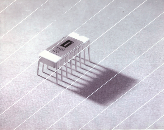

This one is cool because it's cute. Look at that. This thing was completely hand-designed by engineers drawing the shapes of transistor gates on sheets of overhead transparency and exposing pieces of crudely spun silicon to light in a """"cleanroom"""" that would cause most modern fab equipment to swoon like a delicate Victorian lady. Semiconductor manufacturing was maturing at this point but a fab still had more in common with a darkroom for film development than with the mega expensive building sized machines we use today.
As that link above notes, these things were really rough and tumble, and designs were being updated on the scale of weeks as Intel learned, well, how to make chips at an industrial scale. They weren't the first company to do this, in the 60's you could run a chip fab out of a sufficiently well sealed garage, but they were busy building the background that would lead to the next sixty years.
Lisp Chips
This is a family of utterly bullshit prototype processors that failed to be born in the whirlwind days of AI research in the 70's and 80's.
Lisps, a very old but exceedingly clever family of functional programming languages, were the language of choice for AI research at the time. Lisp compilers and interpreters had all sorts of tricks for compiling Lisp down to instructions, and also the hardware was frequently being built by the AI researchers themselves with explicit aims to run Lisp better.
The illogical conclusion of this was attempts to implement Lisp right in silicon, no translation layer.
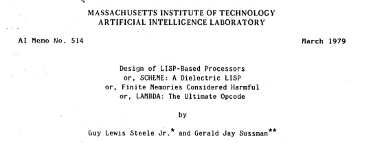
Yeah, that is Sussman himself on this paper.
These never left labs, there have since been dozens of abortive attempts to make Lisp Chips happen because the idea is so extremely attractive to a certain kind of programmer, the most recent big one being a pile of weird designd aimed to run OpenGenera. I bet you there are no less than four members of r/lisp who have bought an Icestick FPGA in the past year with the explicit goal of writing their own Lisp Chip. It will fail, because this is a terrible idea, but damn if it isn't cool.
There were many more chips that bridged this gap, stuff designed by or for Symbolics (like the Ivory series of chips or the 3600) to go into their Lisp machines that exploited the up and coming fields of microcode optimization to improve Lisp performance, but sadly there are no known working true Lisp Chips in the wild.
Zilog Z80
Perhaps the most important chip that ever just kinda hung out. The Z80 was almost, almost the basis of The Future. The Z80 is bizzare. It is a software compatible clone of the Intel 8080, which is to say that it has the same instructions implemented in a completely different way.
This is, a strange choice, but it was the right one somehow because through the 80's and 90's practically every single piece of technology made in Japan contained at least one, maybe two Z80's even if there was no readily apparent reason why it should have one (or two). I will defer to Cathode Ray Dude here: What follows is a joke, but only barely

The Z80 is the basis of the MSX, the IBM PC of Japan, which was produced through a system of hardware and software licensing to third party manufacturers by Microsoft of Japan which was exactly as confusing as it sounds. The result is that the Z80, originally intended for embedded applications, ended up forming the basis of an entire alternate branch of the PC family tree.
It is important to note that the Z80 is boring. It is a normal-ass chip but it just so happens that it ended up being the focal point of like a dozen different industries all looking for a cheap, easy to program chip they could shove into Appliances.
Effectively everything that happened to the Intel 8080 happened to the Z80 and then some. Black market clones, reverse engineered Soviet compatibles, licensed second party manufacturers, hundreds of semi-compatible bastard half-sisters made by anyone with a fab, used in everything from toys to industrial machinery, still persisting to this day as an embedded processor that is probably powering something near you quietly and without much fuss. If you have one of those old TI-86 calculators, that's a Z80. Oh also a horrible hybrid Z80/8080 from Sharp powered the original Game Boy.
I was going to try and find a picture of a Z80 by just searching for it and look at this mess! There's so many of these things.
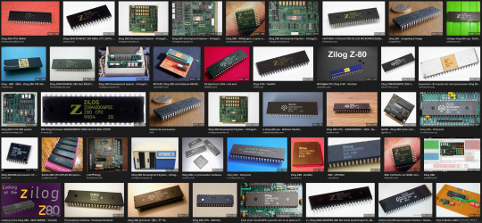
I mean the C/PM computers. The ZX Spectrum, I almost forgot that one! I can keep making this list go! So many bits of the Tech Explosion of the 80's and 90's are powered by the Z80. I was not joking when I said that you sometimes found more than one Z80 in a single computer because you might use one Z80 to run the computer and another Z80 to run a specialty peripheral like a video toaster or music synthesizer. Everyone imaginable has had their hand on the Z80 ball at some point in time or another. Z80 based devices probably launched several dozen hardware companies that persist to this day and I have no idea which ones because there were so goddamn many.
The Z80 eventually got super efficient due to process shrinks so it turns up in weird laptops and handhelds! Zilog and the Z80 persist to this day like some kind of crocodile beast, you can go to RS components and buy a brand new piece of Z80 silicon clocked at 20MHz. There's probably a couple in a car somewhere near you.
Pentium (P6 microarchitecture)
Yeah I am going to bring up the Hackers chip. The Pentium P6 series is currently remembered for being the chip that Acidburn geeks out over in Hackers (1995) instead of making out with her boyfriend, but it is actually noteworthy IMO for being one of the first mainstream chips to start pulling serious tricks on the system running it.

The P6 microarchitecture comes out swinging with like four or five tricks to get around the numerous problems with x86 and deploys them all at once. It has superscalar pipelining, it has a RISC microcode, it has branch prediction, it has a bunch of zany mathematical optimizations, none of these are new per se but this is the first time you're really seeing them all at once on a chip that was going into PC's.
Without these improvements it's possible Intel would have been beaten out by one of its competitors, maybe Power or SPARC or whatever you call the thing that runs on the Motorola 68k. Hell even MIPS could have beaten the ageing cancerous mistake that was x86. But by discovering the power of lying to the computer, Intel managed to speed up x86 by implementing it in a sensible instruction set in the background, allowing them to do all the same clever pipelining and optimization that was happening with RISC without having to give up their stranglehold on the desktop market. Without the P5 we live in a very, very different world from a computer hardware perspective.
From this falls many of the bizzare microcode execution bugs that plague modern computers, because when you're doing your optimization on the fly in chip with a second, smaller unix hidden inside your processor eventually you're not going to be cryptographically secure.
RISC is very clearly better for, most things. You can find papers stating this as far back as the 70's, when they start doing pipelining for the first time and are like "you know pipelining is a lot easier if you have a few small instructions instead of ten thousand massive ones.
x86 only persists to this day because Intel cemented their lead and they happened to use x86. True RISC cuts out the middleman of hyperoptimizing microcode on the chip, but if you can't do that because you've girlbossed too close to the sun as Intel had in the late 80's you have to do something.
The Future
This gets us to like the year 2000. I have more chips I find interesting or cool, although from here it's mostly microcontrollers in part because from here it gets pretty monotonous because Intel basically wins for a while. I might pick that up later. Also if this post gets any longer it'll be annoying to scroll past. Here is a sample from a post I have in my drafts since May:

I have some notes on the weirdo PowerPC stuff that shows up here it's mostly interesting because of where it goes, not what it is. A lot of it ends up in games consoles. Some of it goes into mainframes. There is some of it in space. Really got around, PowerPC did.
237 notes
·
View notes
Text
Cybernetics with Chinese Characteristics & why we suck at the real Grand Strategy Game
Part 2 - The Quickening
Back in 2023, I wrote this more blog-like post about the mid 20th century McCarthyite purges of the Jet Propulsion Laboratory and the knock on effects that had - Namely the inception of the Chinese nuclear program, one-child policy and Chinese computing scene.
Since nothing is new under the sun, we have recently witnessed yet another example of America shooting itself in the foot, yet again, due to it's McCarthyite style purge of Chinese technology.
The release of the Chinese created AI system DeepSeek R1 last week has lead to the largest US stock market loss in history with NVIDIA stock decimated.
A record $465 Billion was wiped off its valuation in a single day. In 2024, the government of Turkey spent this much in a year on it's responsibilities?
Why did this happen?

As always, a lot can be put down to US foreign policy, and the in-intended implications of seemingly positive actions.
Do you want to start a trade war?
Back in the relatively uncontroversial days of the first Trump Presidency (Yes it does feel odd saying that) there were scandals with hardware provided by Chinese company Huawei. This led to the National Defense Authorization Act for Fiscal Year 2019 which explicitly banned Huawei and ZTE's hardware from use in US Government institutions. It also meant the US had to authorise US component manufacturer purchases by these companies.
Crucially this had a 27 month window. This allowed both companies to switch suppliers, and production to domestic suppliers. This actually led to Chinese chip advances. Following on from this came the 2022 move by the US Department of Commerce: "Commerce Implements New Export Controls on Advanced Computing and Semiconductor Manufacturing Items to the People’s Republic of China (PRC) ". This further limited the supply of semiconductor, supercomputer, and similar hardware to the PRC and associated countries.
Ok, well so far this is fairly dry stuff. You might think it would hamper Chinese development and, to some extent, it did.
It also proved to be the main catalyst for one financial quant.
Meet the Quant

Meet Liang Wenfeng (梁文锋). Educated to masters level, Liang was keen to apply machine learning methods to various field, but couldn't get a break. Finally, in the mid 2000's, he settled on a career investigating quantitative trading using machine learning techniques.
He became successful, founding several trading firms based around using machine learning methods, but his interest in base AI never seemed to cease. It was in 2021 that he started purchasing multiple NVIDIA GPUs to create a side project, leading to the creation of DeepSeek in 2023.
Now, due to import limitations, there were limitations on computation. This, however, did not stop DeepSeek's programming team.
Instead they used it as their strength.
Constrains Breed Innovation

For many years, the Western model of AI releases have focussed on making ever larger and larger models.
Why?
Let's break this down from an evolutionary point of view. Modern Western technology companies are largely monopolistic and monolithic. Many of these companies have previously hired staff at higher salaries not to fill roles, but to deny their competitors, and middle market firms, high-flying staff.
They also closely guard trade secrets. What's the training data? What algorithms were used in construction? Guess you'd better chat up some Silicon Valley bros at parties to find out.
For these kinds of firms, having control over large models, housed in data centres makes perfect sense. Controlling model deployment on their own computing systems, and not using local machines, means that they can not only control their systems more carefully, it also means that they can gatekeep access.
If your business model is to allow people to access your models on your servers, and your employees are focussed on making the biggest, best, models, there is no impetus to innovate more efficient, smaller models.
Companies such as OpenAI therefore have the following traits:
Research/Model focus on size over efficiency
Profit driven culture, with emphasis on closed source code
OpenAI's initial focus was as a non-for-profit developing Artificial General Intelligence. This became a for-profit driven company over time. - “I personally chose the price and thought we would make some money.” - Sam Altman
Staff working within paradigm they set in the early 2020's with established code libraries and direct contact with hardware companies creating chips
Significant capital investment - Upwards of several $ billions
DeepSeek, in comparison, is slightly different
For DeepSeek, necessity made innovation necessary. In order to create similar, or better models, than their counterparts, they needed to significantly optimise their code. This requires significantly more work to create, and write, libraries compared to OpenAI.
DeepSeek was started by financial quants, with backgrounds in mainly mathematics and AI. With a focus on mathematics and research, the main drive of many in the company has been exploration of the research space over concerns about profitability.
DeepSeek has also done what OpenAI stopped years ago: actually releasing the code and data for their models. Not only can these models therefore be run via their own gated servers, anyone can replicate their work and make their own system.
For DeepSeek, their traits were:
Research/Model focus on both efficiency and accuracy
Research driven culture, with open nature - “Basic science research rarely offers high returns on investment” - Liang Wenfeng
Strong mathematical background of staff, with ability to work around software, and hardware, constraints
Low capital investment of around $5.5 million

From an evolutionary point of view, DeepSeek's traits have outcompeted those of OpenAI.
More efficient models cost less to run. They also more portable to local machines.
The strong ability of DeepSeek's research focussed staff allowed them to innovate around hardware constraints
Opening up the code to everyone allows anyone (still with the right hardware) to make their own version.
To top it off, the cost to make, and run, DeepSeek R1 is a fraction of the cost of OpenAI's model
House of Cards

Now we can return to today. NVIDIA has lost significant market value. It's not just limited to NVIDIA, but to the entire US technology sector with the most AI adjacent companies losing from 10% to 30% of their valuation in a single day.
The culture, and business model, of OpenAI isn't just limited to OpenAI, but to the entire US technology ecosystem. The US model has been to create rentier-style financial instruments at sky-high valuations.
US tech stocks have been one of the only success stories for America over the past few decades, ever since the offshoring of many manufacturing industries. Like a lost long-unemployed Detroit auto-worker the US has been mainlining technology like Fentanyl, ignoring the anti-trust doctors advice, injecting pure deregulated substances into its veins.
The new AI boom? A new stronger hit, ready for Wall Street, and Private Equity to tie the tourniquet around its arm and pump it right into the arteries.
Like Prometheus, DeepSeek has delved deep and retrieved fire from the algorithmic gods, and shown it's creation to the world. The stock market is on fire, as the traders are coming off of their high, realising they still live in the ruin of barren, decrepit, warehouses and manufactories. The corporate heads, and company leaders reigning over the wreckage like feudal lords, collecting tithes from the serfs working their domain.
A Tale of Two Cities

The rise of DeepSeek isn't just a one-off story of derring-do in the AI world: It's a symbolic representation of the changing world order. DeepSeek is but one company among many who are outcompeting the US, and the world, in innovation.
Where once US free-markets led the world in manufacturing, technology and military capability, now the US is a country devoid of coherent state regulated free-market principles - its place as the singular world power decimated by destroying the very systems which made it great.
"Our merchants and master-manufacturers complain much of the bad effects of high wages in raising the price, and thereby lessening the sale of their goods both at home and abroad. They say nothing concerning the bad effects of high profits. They are silent with regard to the pernicious effects of their own gains. They complain only of those of other people." - Adam Smith, The Wealth of Nations
By selling the jobs of working class communities to overseas businesses, destroying unions and creating rentier based business models without significant anti-trust measures, US business and political elites have sealed the present fate of the country.
The CCP led, but strongly anti-trust enforcing, China has been able to innovate, ironically, using the free-market principles of Adam Smith to rise up and create some of the world's best innovations. The factories, opened by Western business leaders to avoid union/worker labour costs in their own countries, have led Shenzhen, and similar cities, to become hubs of technological innovation - compounding their ability to determine the future of technologies across the world.

Will America be able to regain its position on top? It's too early to say, but the innovative, talented, people who made America in the 20th century can certainly do it again.
As Franklin D. Roosevelt once said: “The liberty of a democracy is not safe if the people tolerated the growth of private power to a point where it becomes stronger than the democratic state itself...
We know now that Government by organized money is just as dangerous as Government by organized mob.
Never before in all our history have these forces been so united against one candidate as they stand today. They are unanimous in their hate for me—and I welcome their hatred.”

Until then, here's a farewell to the American Century 在那之前, 再见美国世���
#cybernetics#cybernetic#ai#artificial intelligence#DeepSeek#OpenAI#ai technology#long reads#politics#us politics
14 notes
·
View notes
Text
The Future of Semiconductors: Unveiling a World of Possibilities
**The Future of Semiconductors: Unveiling a World of Possibilities**
As we stand on the brink of a new era, the semiconductor industry finds itself at the heart of a technological revolution. The impact of semiconductors on our lives has been profound, driving advancements across industries and shaping the very fabric of our modern civilization. But what lies ahead for this dynamic and transformative field? Let's delve into the future of semiconductors and the boundless possibilities that await us.
**1. Quantum Leap in Computing:**
The race towards quantum computing is intensifying, and semiconductors will play a pivotal role in unlocking its true potential. Quantum processors, built on novel semiconductor materials, have the power to process vast amounts of data in a fraction of the time it takes traditional computers. The future of computing will transcend current limitations, empowering us to solve complex problems previously deemed insurmountable.
**2. AI and Machine Learning:**
The era of artificial intelligence is upon us, and semiconductors will serve as the backbone of AI and machine learning applications. With the growing demand for AI-driven technologies in autonomous vehicles, robotics, healthcare, and more, the semiconductor industry is set to witness an unprecedented surge in AI-focused chip designs. Neuromorphic computing, inspired by the human brain's architecture, could unlock revolutionary AI capabilities, paving the way for cognitive computing and self-learning systems.
**3. The Internet of Things (IoT) Revolution:**
As IoT proliferates, the demand for energy-efficient and high-performance semiconductor devices will skyrocket. We envision a future where billions of interconnected devices communicate seamlessly, facilitated by advanced semiconductor technologies. Ultra-low-power processors, sensors, and wireless communication chips will define the landscape of the IoT revolution, shaping smart cities, wearables, and an interconnected world.
**4. Green and Sustainable Semiconductors:**
Sustainability will be a driving force in the semiconductor industry's future. Innovations in materials and manufacturing processes will lead to environmentally friendly and energy-efficient semiconductor solutions. From eco-friendly chip packaging to renewable energy-powered fabs, the industry will strive to minimize its carbon footprint, contributing to a greener tomorrow.
**5. Silicon Photonics and Beyond:**
The integration of photonics with silicon promises a new era of ultra-high-speed data transmission and processing. Silicon photonics will revolutionize data centers, enabling faster communication between chips and reducing data bottlenecks. Moreover, emerging technologies like 2D materials and carbon nanotubes offer exciting possibilities for futuristic semiconductor devices that could outperform traditional silicon-based chips.
**6. Security and Privacy:**
With the increasing dependence on connected devices, security and privacy will be paramount. Future semiconductor designs will prioritize hardware-based security features to protect against cyber threats and safeguard sensitive data. Trusted execution environments and secure enclaves will become integral components of semiconductor devices, ensuring user confidence in an interconnected world.
**7. Global Collaboration and Talent Development:**
The future of semiconductors will thrive on global collaboration and talent development. International partnerships will foster innovation, as countries pool their resources and expertise. Companies will invest in nurturing a diverse and skilled workforce, driving advancements and promoting a culture of inclusion and creativity.
The future of semiconductors is bright, brimming with possibilities that have the potential to redefine our world. As innovators, engineers, and visionaries, let's embrace this transformative journey together. Let's harness the power of semiconductors to build a future that empowers, connects, and inspires generations to come.
*The future is here, and it's in the hands of those who dare to dream and innovate with semiconductors as their guiding light.*
2 notes
·
View notes
Text
Rugged Embedded System Market Faces New Challenges Amid Growing Cybersecurity and Supply Chain Risks
The rugged embedded system market is experiencing robust growth due to increasing demand across defense, industrial, transportation, and energy sectors. These specialized systems are designed to operate reliably in harsh environments—extreme temperatures, vibrations, moisture, dust, and electromagnetic interference. As industries become more digitized and reliant on automation, the need for rugged solutions continues to rise.

Market Overview
Rugged embedded systems are compact, durable computing devices with embedded software tailored for mission-critical applications. Unlike general-purpose computers, these systems prioritize reliability, minimal maintenance, and long life cycles. The market includes hardware (boards, systems, modules) and software (real-time operating systems, middleware), all optimized for rugged performance.
In 2024, the market size is estimated to exceed USD 5 billion, with projections indicating steady growth through 2030. The compound annual growth rate (CAGR) is expected to remain above 7%, driven by sectors that demand continuous operation in extreme conditions.
Key Drivers of Growth
One of the primary growth drivers is the defense and aerospace industry. Military applications, such as battlefield communication systems, drones, and surveillance units, require rugged embedded platforms that function without fail. Governments worldwide continue to invest in smart military infrastructure, further accelerating demand.
Industrial automation is another significant driver. With the rise of Industry 4.0, smart factories rely on rugged embedded systems for controlling robotic systems, monitoring sensor networks, and managing industrial IoT operations. These systems must perform flawlessly in settings where shock, heat, and contamination are constant threats.
The transportation sector also plays a vital role. Railways, maritime fleets, and automotive manufacturers employ rugged systems for fleet management, navigation, engine control, and safety monitoring. As autonomous vehicles and connected infrastructure evolve, the demand for rugged computing systems with enhanced processing power and connectivity grows.
Energy and utilities, especially oil and gas, use rugged embedded systems in offshore rigs, pipeline monitoring, and power grid control. These systems help reduce downtime and enhance safety, offering long-term returns on investment.
Technological Advancements
The rugged embedded system market is evolving rapidly with technological innovations. The integration of AI and machine learning into rugged systems is a notable trend, enabling predictive maintenance, real-time analytics, and adaptive control systems.
Additionally, the move towards modular and scalable architectures allows developers to customize systems for specific applications while reducing time-to-market. These platforms are increasingly leveraging edge computing, enabling data processing at the source rather than relying on centralized cloud infrastructure. This improves response times and minimizes the risks associated with network latency or outages.
5G connectivity is also being introduced into rugged systems, enhancing real-time data transmission and supporting advanced applications like augmented reality for field maintenance and operations.
Market Challenges
Despite strong growth, several challenges persist. High development and production costs can hinder adoption, especially for small- and medium-sized enterprises. Designing systems that meet stringent environmental and safety certifications, such as MIL-STD-810 and IP ratings, requires substantial R&D investment.
Supply chain disruptions, particularly in semiconductor components, can delay manufacturing and increase costs. The market also faces increasing pressure to balance performance with power efficiency, particularly in remote or mobile applications with limited access to power sources.
Furthermore, cybersecurity concerns are rising as rugged systems become more connected. Protecting these systems from cyber threats is crucial, especially in critical infrastructure and defense applications.
Regional Insights
North America holds a dominant share of the rugged embedded system market, primarily due to its advanced defense sector and strong presence of key players. Europe follows closely, with major contributions from aerospace and rail transportation industries. The Asia-Pacific region, particularly China, Japan, and India, is expected to witness the fastest growth due to rapid industrialization, expanding defense budgets, and infrastructure development.
Future Outlook
The rugged embedded system market is poised for sustained expansion, fueled by growing demand for reliable computing in harsh environments. As digital transformation accelerates across sectors, the market will continue to evolve, with a strong focus on AI integration, edge intelligence, and modular design.
Companies that invest in innovation, offer flexible customization, and meet evolving industry standards will be well-positioned to lead in this competitive landscape. Despite challenges, the long-term outlook for the rugged embedded system market remains optimistic.
0 notes
Text
🌐 Semiconductor Market Set to Triple by 2032, Surpassing $2.06 trillion. Here's What's Driving It.
Recent market analyses indicate a robust growth trajectory for the semiconductor industry, projecting a significant expansion over the next decade.
📈 Semiconductor Market Forecast (2024–2032)
2024 Market Size: $681.05 billion
2025 Projection: $755.28 billion
2032 Forecast: $2,062.59 billion
CAGR (2024–2032): 15.4%
This represents nearly a 3x growth in just eight years.

🌍 Asia-Pacific Leads the Charge
In 2024, the Asia-Pacific region accounted for approximately 52.93% of the global semiconductor market, driven by countries like Taiwan, South Korea, and China. These nations are investing heavily in semiconductor manufacturing and R&D to maintain their competitive edge.
🔑 Key Drivers Behind the Growth
Artificial Intelligence (AI) and Machine Learning The surge in AI applications, from data centers to edge devices, is fueling demand for advanced semiconductors capable of handling complex computations.
5G and IoT Expansion The global rollout of 5G networks and the proliferation of Internet of Things (IoT) devices require a vast array of semiconductors, from RF chips to sensors.
Automotive Industry Transformation The shift towards electric vehicles (EVs) and autonomous driving technologies is increasing the semiconductor content per vehicle, driving substantial market growth.
Government Initiatives and Investments Policies like the U.S. CHIPS Act and similar initiatives in Europe and Asia are injecting billions into domestic semiconductor production, aiming to bolster supply chain resilience.
Emerging Technologies Advancements in areas like quantum computing, augmented reality (AR), and virtual reality (VR) are creating new avenues for semiconductor applications.
💡 Implications for Stakeholders
For Innovators: The evolving landscape presents opportunities to develop specialized chips tailored for AI, 5G, and other emerging applications.
For Investors: The semiconductor sector's projected growth underscores its potential for substantial returns, particularly in companies leading in innovation and manufacturing capabilities.
0 notes
Text
Why Is Electronics and Communication Engineering in Hyderabad Ideal for Aspiring Engineers?

Electronics and Communication Engineering (ECE) has long been regarded as one of the most versatile and in-demand engineering disciplines in India and globally. Among the many cities offering high-quality education in ECE, Hyderabad stands out due to its strong academic infrastructure, flourishing tech industry, and dynamic learning environment. For students looking to pursue Electronics and Communication Engineering in Hyderabad, institutions like HITAM (Hyderabad Institute of Technology and Management) offer a holistic and industry-relevant curriculum that equips graduates with the skills to thrive in today’s competitive landscape.
In this post, we’ll explore why Hyderabad, particularly HITAM, is becoming a hotspot for ECE education.
Why Choose Electronics and Communication Engineering?
Before diving into Hyderabad-specific advantages, it’s important to understand the appeal of ECE as a career path.
ECE blends principles of electrical engineering and computer science, offering a wide scope in sectors such as:
- Telecommunications
- Embedded Systems
- Signal Processing
- Consumer Electronics
- Robotics and Automation
- Semiconductor Industry
- IoT (Internet of Things)
- AI and Machine Learning
Graduates can work as design engineers, communication analysts, embedded systems developers, or research scientists in the public and private sectors.
Why Hyderabad for ECE?
Hyderabad has become a tech powerhouse in India, with a thriving ecosystem of IT parks, electronics manufacturing hubs, and R&D centers. The city’s growth in these sectors directly complements ECE students' training.
Here are some compelling reasons to study Electronics and Communication Engineering in Hyderabad:
1) Thriving Tech Ecosystem: Hyderabad is home to major global and Indian tech giants like Qualcomm, Intel, Microsoft, and TCS. These companies actively recruit engineering graduates, especially those with a background in ECE.
2) Startup Culture: The city has a robust startup ecosystem, supported by initiatives like T-Hub and WE-Hub. ECE students interested in entrepreneurship find Hyderabad to be a nurturing ground for innovation and prototyping.
3) Academic Excellence: Institutes like HITAM are leading the way in providing a future-ready engineering education. HITAM, in particular, emphasizes experiential learning, industry internships, and research-focused study, preparing students for both jobs and higher education.
4) Smart City Advantage: Hyderabad is rapidly transforming into a smart city, with IoT-based urban infrastructure and smart grids—areas directly related to ECE. Students gain practical exposure to these developments, enhancing real-world learning.
Why HITAM for Electronics and Communication Engineering?
HITAM is a NAAC-accredited institution and an emerging name among the top engineering colleges in Hyderabad. It offers a highly relevant and innovative ECE program integrating academic knowledge with practical application.
Let’s look at the factors that set HITAM apart:
1) Outcome-Based Education: HITAM follows a strong Outcome-Based Education (OBE) model aligned with NBA accreditation standards. This approach ensures that students graduate with demonstrable problem-solving, innovation, and project management skills.
2) Industry-Aligned Curriculum: HITAM’s ECE curriculum is frequently updated in collaboration with industry experts. Students are trained in modern tools like MATLAB, VHDL, Python, and machine learning technologies relevant to ECE.
3) Project-Based Learning: HITAM emphasizes hands-on, project-based learning (PBL). Students work on real-world problems, sometimes collaborating with industry partners, building portfolios that make them job-ready.
4) Advanced Laboratories: HITAM boasts state-of-the-art labs for embedded systems, digital signal processing, IoT, and VLSI design. These labs provide a rich environment for experimentation, prototyping, and research.
5) Research and Innovation: HITAM encourages undergraduate research through its Innovation & Entrepreneurship Development Cell (IEDC). ECE students regularly participate in hackathons, publish papers, and receive funding for tech innovations.
6) Placement Support: HITAM has a strong placement cell with established links to the electronics and IT industries. Students from the ECE stream have secured roles in companies like Infosys, Capgemini, Tech Mahindra, and startups working in IoT and automation.
7) Ethical and Sustainable Learning: In addition to technical excellence, HITAM instills sustainability, ethics, and leadership values—essential traits in today’s engineering landscape.
Future Scope for ECE Graduates from Hyderabad
Graduating with an ECE degree from Hyderabad opens doors in multiple industries. Some of the future-focused roles include:
- AI Hardware Engineer
- Communication Network Designer
- IoT Systems Architect
- Embedded System Developer
- VLSI Chip Designer
- Wireless Protocol Engineer
The Indian government’s push for "Make in India" and Digital India has further boosted the demand for skilled ECE professionals, particularly in electronics design and manufacturing.
Additionally, Hyderabad’s expanding aerospace, defense, and smart manufacturing sectors seek professionals with ECE expertise.
Conclusion
Studying Electronics and Communication Engineering in Hyderabad is a smart decision for any engineering aspirant. With its vibrant tech ecosystem, high-quality academic institutions like HITAM, and strong industry collaboration, Hyderabad provides everything a student needs to grow into a competent and successful ECE professional.
If you’re passionate about blending technology with communication systems, innovating solutions, and working on cutting-edge technologies, pursuing ECE at an institution like HITAM will give you the strong foundation and exposure you need.
Explore HITAM’s ECE program and take your first step toward a future in advanced electronics and communication. 👉 Visit: https://hitam.org/electronics-and-communication-engineering/ to learn more.
0 notes
Text
The Role of Semiconductors in the nasdaq 100 index
The nasdaq 100 index serves as a focused snapshot of the largest non-financial companies listed on the Nasdaq Stock Market. Heavily tilted toward sectors such as technology, consumer services, and health sciences, this index captures the rhythm of innovation-led enterprises that shape the global digital economy.
Performance Anchored in Technology
The nasdaq 100 index is largely driven by technology-oriented firms that specialize in hardware, software, digital platforms, and cloud-based infrastructure. These companies often feature at the cutting edge of artificial intelligence, data processing, and next-generation connectivity.
Tech manufacturers, from semiconductor giants to specialized chip designers, contribute significantly to index fluctuations. Their performance is frequently influenced by product demand cycles, international supply chain dynamics, and advances in computing capabilities.
Communications and Platform Evolution
Digital communication companies within the nasdaq 100 index continue to evolve in response to changing consumption patterns. The surge in content streaming, virtual conferencing, and social media interaction has added depth to the index’s digital ecosystem.
These firms leverage vast user networks and scalable software frameworks to grow platform reach and efficiency. The influence of these platforms on the index is heightened by their integration into both consumer lifestyles and enterprise workflows.
Health Innovation and Biotechnology
Another area shaping the nasdaq 100 index involves companies in biotechnology and health technology. These entities work across genomics, diagnostics, and therapeutic solutions, often undergoing product trials and research phases before reaching regulatory clearance.
Their performance can have episodic effects on the broader index, especially when breakthrough studies or approvals take place. While the health segment is relatively smaller than technology within the index, its contributions can provide balance and diversity in momentum.
Retail Transformation and Consumer Trends
Retail-focused digital brands in the nasdaq 100 index have experienced strong shifts as consumer behavior adapts to e-commerce and mobile-first interaction. These companies are typically involved in direct-to-consumer models and depend heavily on logistical agility and customer analytics.
Seasonal demand changes, pricing strategies, and platform enhancements often shape performance for these names. As more retail transitions to cloud and mobile formats, the consumer technology space is expected to remain prominent within the index.
Data Infrastructure and Cloud Services
A cornerstone of the nasdaq 100 index remains its cloud and infrastructure service providers. These companies offer services for enterprise storage, workflow automation, and remote computing—all of which underpin the digital economy.
From small businesses to global corporations, demand for scalable infrastructure continues to rise. Consequently, enterprise-grade solutions in networking, cybersecurity, and SaaS have gained a stable presence across the index's top listings.
Artificial Intelligence and Machine Learning Integration
AI has emerged as a pivotal catalyst influencing activity within the nasdaq 100 index. Whether through autonomous systems, AI-powered analytics, or speech recognition, multiple companies are embedding machine learning into their operations.
These efforts contribute not only to efficiency but also to new product verticals, strategic alliances, and R&D commitments. The pace of AI adoption has become a trend closely monitored by market participants when evaluating the trajectory of the index.
Environmental Tech and Clean Data
Several companies in the nasdaq 100 index have begun integrating energy-efficient operations and sustainability-based solutions. These include data centers with lower carbon footprints and cloud infrastructure designed for optimal energy use.
This trend reflects broader corporate strategies around environmental compliance, technological responsibility, and stakeholder alignment—factors that increasingly define long-term business narratives.
Market Sensitivity and Sector Movements
The performance of the nasdaq 100 index is also influenced by macro-level indicators such as inflation trends, monetary policies, and international trade developments. Because the index features globally recognized corporations, it is sensitive to changes in supply logistics, regulatory frameworks, and policy shifts abroad.
Sector rotation, particularly between cyclical and defensive segments, can also influence daily and weekly trends within the index. Observers continue to track how market sentiment aligns with the fundamental strength of technology and services firms included in the index.
The nasdaq 100 index encapsulates a dynamic cross-section of high-growth, non-financial firms that drive digital transformation worldwide. From foundational hardware providers to cutting-edge cloud innovators, the index reflects evolving trends across enterprise technology, consumer behavior, and scientific advancement.
0 notes
Text
X-ray Inspection System Market to Reach $1.3 Billion by 2034: Key Growth Trends

The global X-ray inspection system market was valued at US$ 820.0 million in 2023 and is projected to grow at a compound annual growth rate (CAGR) of 4.5% from 2024 to 2034, reaching approximately US$ 1.3 billion by the end of the forecast period. X-ray inspection systems utilize high-energy electromagnetic radiation to penetrate materials, create detailed images of internal structures and detect foreign objects or defects in finished goods. Widely adopted in food and beverage, pharmaceutical, electronics, aerospace, automotive and security sectors, these systems are prized for their non-destructive testing capability, high throughput and automated data analysis.
Market Drivers & Trends
Food Safety and Compliance: As global regulatory standards tighten (e.g., HACCP, FDA FSMA), food and beverage processors increasingly rely on X-ray inspection to detect contaminants metal, glass, stone and dense organic matter without damaging products or packaging. Non-destructive X-ray scanning helps lower recall risk, reduce waste and maintain brand reputation.
Security Applications: Rising threats from smuggling operations at ports and airports to screening in public buildings are driving demand for advanced X-ray security systems with real-time threat algorithms. Governments worldwide are allocating larger budgets for state-of-the-art X-ray checkpoint scanners.
Technological Advancements: Integration of artificial intelligence (AI) and machine learning (ML) enables automated pattern recognition, reducing false positives and operator intervention. The rise of 3D computed tomography (CT) X-ray systems offers volumetric inspection, delivering a complete internal view for precision industries such as aerospace and semiconductors.
Industry 4.0 Integration: Network-enabled “smart factories” leverage X-ray systems with IoT connectivity for continuous process monitoring, predictive maintenance and centralized quality control dashboards.
Latest Market Trends
3D Imaging Adoption: Leading vendors are rolling out affordable CT-based X-ray scanners that provide layer-by-layer inspection. This trend is particularly strong in electronics and pharmaceutical packaging, where minute defect detection is critical.
High-Throughput Lines: To meet the demands of e-commerce and fast-moving consumer goods, manufacturers are deploying multi-lane X-ray conveyors that can inspect hundreds of units per minute.
Compact, Modular Designs: Smaller form-factor X-ray units with quick-swap detectors allow manufacturers to retrofit existing lines with minimal downtime.
Sustainability Focus: New models consume up to 30% less energy and feature advanced shielding materials for safer, eco-friendly operation.
Key Players and Industry Leaders
METTLER TOLEDO
Nordson Corporation
Comet Group
Anritsu
Viscom SE
North Star Imaging Inc.
Nikon Corporation
ISHIDA CO., LTD.
OMRON Corporation
TOSHIBA IT & CONTROL SYSTEMS CORPORATION
3DX-RAY
Sesotec GmbH
Visiconsult GmbH
Scienscope
Recent Developments
July 2023: Nikon Americas Inc. acquired Avonix Imaging LLC to enhance its digital CT inspection portfolio, strengthening its position in industrial metrology.
May 2023: Mettler-Toledo launched the X2 Series, democratizing high-performance X-ray inspection for small and mid-sized food processors with an attractive price-performance ratio and extended service life.
September 2022: Mettler-Toledo introduced a next-generation low-density contaminant detection algorithm, improving identification of plastics and other soft materials in packaged foods.
Other strategic partnerships and product launches throughout 2024 signal an industry pivot toward AI-enabled, cloud-connected X-ray platforms.
Market New Opportunities and Challenges
Opportunities:
Emerging Economies: Rapid expansion of packaged-food and pharmaceutical industries in Asia Pacific and Latin America presents untapped demand for inspection systems.
Custom Solutions: Growing need for tailor-made inspection equipment e.g., for novel packaging formats—creates value-added service opportunities.
After-Sales Services: Predictive maintenance contracts and software upgrades offer recurring revenue streams for OEMs.
Challenges:
High Capital Expense: Initial investment and regulatory approval costs can deter small and medium enterprises.
Technological Complexity: Integrating AI/ML and CT functionality requires specialized expertise, potentially slowing adoption.
Regulatory Variability: Differing international standards necessitate customizable system configurations, complicating product roadmaps.
Future Outlook
Over the next decade, the X-ray inspection market will be defined by deeper AI integration, miniaturized hardware and flexible, plug-and-play architectures. As throughput demands rise particularly in automated e-commerce packing facilities systems capable of inspecting multiple lines simultaneously will gain traction. Continued investments in R&D will lower per-unit cost and enhance detection of low-density contaminants. By 2034, the proliferation of Industry 4.0 ecosystems will position X-ray inspection as a cornerstone technology for end-to-end digital quality control.
Explore core findings and critical insights from our Report in this sample - https://www.transparencymarketresearch.com/sample/sample.php?flag=S&rep_id=35627
Market Segmentation
Segment
Sub-segments
Type
Digital Imaging, Film-based Imaging
Dimension
2D, 3D
Function
Manual, Automated
End-use
Electronics & Semiconductors; Oil & Gas; Aerospace; Government Infrastructure; Automotive; Power Generation; Food & Pharmaceuticals; Packaging; Others
Region
North America; Europe; Asia Pacific; Middle East & Africa; South America
Regional Insights
Asia Pacific: Held the largest share in 2023, driven by stringent food safety regulations, booming packaged-food consumption and rapid pharmaceutical industry growth in China and India.
North America: Continues to invest heavily in airport/port security and high-tech manufacturing, supporting robust market expansion.
Europe: Emphasizes sustainability and energy efficiency, prompting vendors to introduce eco-friendly X-ray systems.
Middle East & Africa / South America: Emerging security and food safety infrastructure projects are creating early adopter markets.
Why Buy This Report?
Comprehensive Analysis: In-depth coverage of market drivers, restraints, opportunities and emerging trends through 2034.
Strategic Insights: Analyst viewpoints on technology adoption, competitive landscape and regulatory impacts.
Data-Rich: Quantitative forecasts by segment, region and end-use, plus historical data from 2020–2022.
Vendor Profiles: Detailed company overviews, product portfolios, financials and strategic developments of leading players.
Actionable Recommendations: Guidance on market entry, pricing strategies and partnership opportunities for OEMs, investors and end-users.
This electronic (PDF) + Excel package equips decision-makers with the intelligence needed to gain competitive advantage in the dynamic X-ray inspection system market.
Frequently Asked Questions
Q1. What is driving the rapid adoption of X-ray inspection in the food industry? A: Stricter food safety regulations (e.g., HACCP, FDA), consumer demand for contaminant-free products and the need to minimize recalls and waste.
Q2. How does 3D CT X-ray inspection improve upon traditional 2D systems? A: 3D CT systems provide volumetric imaging, enabling detection of defects at any depth and offering comprehensive analysis of complex assemblies.
Q3. Which regions offer the highest growth potential through 2034? A: Asia Pacific, driven by rapid urbanization, expansion of packaged-food and pharmaceutical sectors, and government investments in quality infrastructure.
Q4. Are AI and machine learning capabilities standard in modern X-ray inspection systems? A: Leading suppliers now integrate AI/ML for pattern recognition and automated defect classification, though adoption varies by industry and budget.
Q5. What are the key barriers to entry for new players in this market? A: High R&D costs, regulatory approvals and the technical complexity of integrating advanced imaging modalities and analytics.
About Transparency Market Research Transparency Market Research, a global market research company registered at Wilmington, Delaware, United States, provides custom research and consulting services. Our exclusive blend of quantitative forecasting and trends analysis provides forward-looking insights for thousands of decision makers. Our experienced team of Analysts, Researchers, and Consultants use proprietary data sources and various tools & techniques to gather and analyses information. Our data repository is continuously updated and revised by a team of research experts, so that it always reflects the latest trends and information. With a broad research and analysis capability, Transparency Market Research employs rigorous primary and secondary research techniques in developing distinctive data sets and research material for business reports. Contact: Transparency Market Research Inc. CORPORATE HEADQUARTER DOWNTOWN, 1000 N. West Street, Suite 1200, Wilmington, Delaware 19801 USA Tel: +1-518-618-1030 USA - Canada Toll Free: 866-552-3453 Website: https://www.transparencymarketresearch.com Email: [email protected]
0 notes
Text
Photomask Inspection Market Future Outlook Driven by Technological Innovation and Rising Semiconductor Demand
The photomask inspection market future outlook is highly optimistic, fueled by growing demand in the semiconductor industry and rapid innovation in inspection technologies. As chip designs become increasingly complex and feature sizes shrink, the need for high-precision photomask inspection solutions becomes more critical than ever. Photomask inspection market technologies are evolving to meet the stringent quality control standards demanded by manufacturers aiming for zero-defect production.
Photomasks, essential in the photolithography process of chip fabrication, act as stencils that transfer intricate circuit patterns onto wafers. Any defect in a photomask can lead to significant losses due to faulty chips, hence the rising importance of accurate and reliable inspection tools. With the global push towards advanced nodes, the margin for error has decreased, making photomask inspection a vital part of the manufacturing pipeline.

Technological Advancements Fueling Market Growth
One of the main forces driving the photomask inspection market is technological innovation. The shift towards EUV (Extreme Ultraviolet Lithography) in semiconductor manufacturing is increasing the complexity of photomasks, which now require more advanced inspection systems. Traditional inspection methods are proving inadequate for these cutting-edge technologies, paving the way for the adoption of sophisticated techniques such as e-beam inspection and deep learning-based defect detection.
Moreover, artificial intelligence and machine learning are being integrated into inspection systems to enhance speed and accuracy. These technologies enable faster analysis of large datasets generated during inspections and help identify patterns or defects that may go unnoticed with conventional methods.
Rising Demand in Consumer Electronics and Automotive Sectors
The growing use of semiconductors in consumer electronics, automotive applications, and industrial equipment is significantly boosting the photomask inspection market. Smartphones, smart TVs, IoT devices, and electric vehicles all rely on complex semiconductor chips. This surging demand translates to higher production volumes and a need for stringent quality checks at every stage, including photomask inspection.
In the automotive sector, especially with the rise of electric and autonomous vehicles, the requirement for flawless chip performance is even more crucial. Photomask inspection ensures that only high-quality masks are used in chip production, minimizing the risk of defects and improving reliability.
Regional Market Insights
Asia-Pacific continues to dominate the photomask inspection market, primarily due to the presence of major semiconductor manufacturing hubs in countries like Taiwan, South Korea, China, and Japan. These regions house leading foundries and integrated device manufacturers that consistently invest in advanced inspection technologies.
North America also plays a vital role, driven by strong R&D capabilities and the presence of key technology providers. Europe, with its focus on industrial automation and automotive innovation, contributes significantly as well, especially in terms of demand for high-precision chips.
Challenges and Restraints
Despite its positive outlook, the photomask inspection market faces several challenges. One major concern is the high cost associated with advanced inspection equipment. The development and maintenance of these systems require significant investment, which can be a barrier for smaller semiconductor manufacturers.
Additionally, as inspection technology becomes more advanced, there is a growing need for skilled personnel to operate and interpret the systems accurately. The shortage of such talent could slow down adoption rates among manufacturers looking to implement the latest inspection solutions.
Future Opportunities and Strategic Developments
Looking ahead, the market presents vast opportunities, especially in niche areas such as 3D integrated circuits, AI chips, and quantum computing. These specialized chips demand ultra-high precision during fabrication, thereby elevating the importance of photomask inspection.
Partnerships and collaborations between semiconductor companies and inspection equipment providers are also expected to drive innovation. Strategic mergers and acquisitions could further consolidate technological capabilities and expand market reach.
As sustainability becomes a growing concern, companies are also exploring eco-friendly inspection technologies that minimize energy consumption and reduce waste. This green shift, though still emerging, could open new pathways for growth in the market.
Conclusion
The future outlook for the photomask inspection market is marked by continuous innovation, increasing demand across industries, and strategic technological integration. As the semiconductor industry pushes the boundaries of performance and miniaturization, photomask inspection will remain a critical enabler of progress. Companies investing in advanced inspection tools and embracing next-generation technologies will be best positioned to thrive in this rapidly evolving landscape.
0 notes
Text
Quantum Computing Market Size, Share, Trends, Demand, Growth, Challenges and Competitive Outlook
Global Quantum Computing Market - Size, Share, Demand, Industry Trends and Opportunities
Global Quantum Computing Market, By System (Single Qubit Quantum System, Multiple Qubit System), Qubits (Trapped Ion Qubits, Semiconductor Qubits and Super Conducting), Offering (Systems, Services), Deployment Model (On-Premises, Cloud), Component (Hardware, Software and Services), Application (Cryptography, Simulation, Parallelism, Machine Learning, Algorithms, Others), Logic Gates (Toffoli Gate, Hadamard Gate, Pauli Logic Gates and Others), Verticals (Banking and Finance, Healthcare and Pharmaceuticals, Defense, Automotive, Chemical, Utilities, Others) – Industry Trends.
Access Full 350 Pages PDF Report @
**Segments**
- **Technology**: The quantum computing market can be segmented based on different technologies such as superconducting, trapped ions, semiconductor, and others. Superconducting technology is currently the most widely used technology in quantum computing due to its relatively easier scalability and lower error rates. Trapped ions technology is known for high coherence times and low error rates, making it suitable for certain applications. Semiconductor-based quantum computing is also gaining traction due to its potential to leverage existing semiconductor manufacturing processes.
- **Application**: Another key segment is based on applications such as optimization, machine learning, cybersecurity, and others. Optimization applications are one of the earliest and most prominent use cases for quantum computing, where it can significantly outperform classical computers in solving complex optimization problems. Machine learning is another rapidly growing application area, where quantum computing can enhance algorithms and speed up training processes. Cybersecurity is also emerging as a critical application due to the potential of quantum computers to break traditional encryption methods.
- **End-User**: The quantum computing market can also be segmented based on end-users such as healthcare, finance, defense, automotive, and others. Healthcare industry is exploring quantum computing for drug discovery, genomics, and personalized medicine. Finance sector is leveraging quantum computing for risk assessment, portfolio optimization, and algorithmic trading. Defense industry is interested in quantum computing for secure communications, cryptography, and battlefield simulations. Automotive sector is exploring quantum computing for vehicle design, supply chain optimization, and autonomous driving.
**Market Players**
- **IBM**: IBM is a key player in the quantum computing market with its IBM Q Network offering access to its quantum computers via the cloud. The company is actively involved in quantum research and developing quantum algorithms for various industries.
- **Google**: Google has made significant advancements in quantum computing with its 72-qubit Bristlecone processor and the quest for quantum supremacy. The company is working on developing practical quantum algorithms and applications.
- **Microsoft**: Microsoft is investing heavily in quantum computing research through itsIn the rapidly evolving quantum computing market, segmentation plays a crucial role in understanding the diverse dynamics and potential opportunities within the industry. The segmentation based on technology provides insights into the different approaches and methodologies utilized in quantum computing systems. Superconducting technology stands out as a widely adopted approach due to its scalability and relatively lower error rates. Trapped ions technology, on the other hand, offers high coherence times and minimal error rates, making it suitable for specific applications that require high precision. Semiconductor-based quantum computing is gaining momentum as it leverages existing semiconductor manufacturing processes, offering a unique pathway for integration into the mainstream technology landscape.
The segmentation based on applications highlights the diverse use cases and potential impact of quantum computing across various industries. Optimization applications have been a cornerstone of quantum computing, demonstrating superior performance in solving complex optimization problems compared to classical computers. Machine learning is rapidly becoming a key application area, with quantum computing showcasing the potential to enhance algorithms and accelerate training processes in data-intensive environments. Cybersecurity has emerged as a critical application due to the threat quantum computers pose to traditional encryption methods, driving the need for advanced security solutions.
End-user segmentation delves into the specific industries that are leveraging quantum computing technology to drive innovation and address industry-specific challenges. In the healthcare sector, quantum computing is being explored for applications such as drug discovery, genomics, and personalized medicine, showcasing the potential to revolutionize healthcare delivery and patient outcomes. The finance industry is harnessing quantum computing for risk assessment, portfolio optimization, and algorithmic trading, seeking to gain a competitive edge through enhanced computational capabilities. The defense sector is focusing on quantum computing for secure communication, cryptography, and simulations to bolster national security and strategic decision-making. The automotive industry is exploring quantum computing for applications in vehicle design, supply chain optimization, and autonomous driving, aiming to enhance efficiency and drive innovation in the mobility landscape.
Market players such as IBM, Google, and Microsoft are at the forefront of driving innovation and shaping the future of quantum computing. IBM's IBM Q**Segments**
- **Technology**: The quantum computing market can be segmented based on different technologies such as superconducting, trapped ions, semiconductor, and others. Superconducting technology is currently the most widely used technology in quantum computing due to its relatively easier scalability and lower error rates. Trapped ions technology is known for high coherence times and low error rates, making it suitable for certain applications. Semiconductor-based quantum computing is also gaining traction due to its potential to leverage existing semiconductor manufacturing processes.
- **Application**: Another key segment is based on applications such as optimization, machine learning, cybersecurity, and others. Optimization applications are one of the earliest and most prominent use cases for quantum computing, where it can significantly outperform classical computers in solving complex optimization problems. Machine learning is another rapidly growing application area, where quantum computing can enhance algorithms and speed up training processes. Cybersecurity is also emerging as a critical application due to the potential of quantum computers to break traditional encryption methods.
- **End-User**: The quantum computing market can also be segmented based on end-users such as healthcare, finance, defense, automotive, and others. Healthcare industry is exploring quantum computing for drug discovery, genomics, and personalized medicine. Finance sector is leveraging quantum computing for risk assessment, portfolio optimization, and algorithmic trading. Defense industry is interested in quantum computing for secure communications, cryptography, and battlefield simulations. Automotive sector is exploring quantum computing for vehicle design, supply chain optimization, and autonomous driving.
**Market Players**
-
Core Objective of Quantum Computing Market:
Every firm in the Quantum Computing Market has objectives but this market research report focus on the crucial objectives, so you can analysis about competition, future market, new products, and informative data that can raise your sales volume exponentially.
Size of the Quantum Computing Market and growth rate factors.
Important changes in the future Quantum Computing Market.
Top worldwide competitors of the Market.
Scope and product outlook of Quantum Computing Market.
Developing regions with potential growth in the future.
Tough Challenges and risk faced in Market.
Global Quantum Computing-top manufacturers profile and sales statistics.
Highlights of TOC:
Chapter 1: Market overview
Chapter 2: Global Quantum Computing Market
Chapter 3: Regional analysis of the Global Quantum Computing Market industry
Chapter 4: Quantum Computing Market segmentation based on types and applications
Chapter 5: Revenue analysis based on types and applications
Chapter 6: Market share
Chapter 7: Competitive Landscape
Chapter 8: Drivers, Restraints, Challenges, and Opportunities
Chapter 9: Gross Margin and Price Analysis
How the Report Aids Your Business Discretion?
This section of this Market report highlights some of the most relevant factors and growth enablers that collectively ensure a high-end growth spurt
The report unravels details on pronounced share assessments across both country-wise as well as region-based segments
A leading synopsis of market share analysis of dynamic players inclusive of high-end industry veterans
New player entry analysis and their scope of new business models
The report includes strategic recommendations for new business veterans as well as established players seeking novel growth avenues
A detailed consultation services based on historical as well as current timelines to ensure feasible forecast predictions
A thorough evaluation and detailed study of various segments as well as sub-segments across regional and country-specific developments
Details on market estimations, market size, dimensions
A review of market competitors, their high-end product and service portfolios, dynamic trends, as well as technological advances that portray high end growth in this Market
Browse Trending Reports: Waterproof Coatings and Membranes Market Homogenizers Market Nitric Acid Market Vaginitis Therapeutics Market Non-Stick Cookware Market Hybrid and Community Cloud as a Service Market Automotive Multi Axis Positions Sensors Market Natural Spirits Market Coronavirus Test Kits Market High Performance Lubricant Market Disposable Tea Flask Market
About Data Bridge Market Research:
Data Bridge set forth itself as an unconventional and neoteric Market research and consulting firm with unparalleled level of resilience and integrated approaches. We are determined to unearth the best market opportunities and foster efficient information for your business to thrive in the market. Data Bridge endeavors to provide appropriate solutions to the complex business challenges and initiates an effortless decision-making process.
Contact Us:
Data Bridge Market Research
US: +1 614 591 3140
UK: +44 845 154 9652
APAC : +653 1251 975
Email: [email protected]
0 notes
Text
Equal1’s Bell-1: New Silicon Quantum Server For Data Centers

The Bell-1 Quantum Server, launched by Irish firm Equal1, is a quantum computing milestone. The Bell-1 is the first rack-mounted silicon quantum computer, designed for High-Performance Computing (HPC) data centres. Quantum Computing 2.0, launched by Equal1, seeks to make this powerful technology more accessible than ever.
Instead of the large, complicated installations used in prior quantum computers, the Bell-1 is designed for practical usage and easy integration into the data centre architecture. Corporate executives unveiled Bell-1 on March 16.
Standard requirements and compact size For Data Centres
Top features of the Bell-1 are its operating needs and form factor, which mesh well with regular IT environments. The Bell-1 Quantum Server may be put on data centre racks due to its standard size and rack-mountability. Its size is comparable to GPU servers. It weighs slightly over 440 pounds (200 kilogrammes), yet it's rack-mounted and fits in any rack space.
Unlike typical quantum systems, the Bell-1 does not need specialist infrastructure. Simply plug it into a 110V/220V single-phase outlet. Its 1600 W power consumption is comparable to a top GPU server and extremely low for a quantum computer. This shows far lower energy use than many traditional quantum devices.
Innovative Cooling: Self-Contained Cryogenics
The Bell-1's integrated closed-cycle cryocooler is a key engineering breakthrough. Quantum operations need extremely low temperatures, which have typically required large, external dilution freezers and complex cooling systems. Bell-1 cooling is contained in its rack-mounted container.
This unique self-contained mechanism lets the Bell-1 operate at 0.3 Kelvin. 0.3 Kelvin is near absolute zero at -459.13 F or 272.85 C. This ultra-low temperature requires no cooling infrastructure or equipment, simplifying deployment.
The Basics of Silicon Spin Qubits
Silicon-based spin qubits are a major Bell-1 technological choice. This contrasts with trapped-ion or superconducting qubit quantum computing systems.
Bell-1 presently has six qubits. Spin qubits made of silicon are advantageous. Smaller silicon-based qubits allow more qubits per device. This technique can also use semiconductor manufacturing methods. Interoperability with well-established manufacturing processes indicates scalability and dependability that novel fabrication techniques may struggle with. Qubit control and lengthy coherence are possible with pure silicon manufacturing. Complex quantum algorithms and calculations need coherence time, a qubit's capacity to exist in several quantum states.
The Bell-1's main chip, the Unity 6-Qubit Quantum Processing System, uses spin qubits.
Classical and Quantum Processing on One Chip
Future generations are expected to complete the Bell-1's architectural breakthrough of several processing units on a single chip. The newest technology features quantum processor units (QPUs) together with Arm CPUs, which are efficient and compact, and neural processing units (NPUs), which accelerate artificial intelligence and machine learning.
Putting these components on a chip is a major step. It aims to eliminate the complex coordination needed to govern processing and communication among conventional and quantum computing components. This comprehensive technique is designed to integrate with AI and HPC systems for powerful, on-demand quantum acceleration.
Enhancing Current Developments and Error Correction
Equal1 tried silicon-based quantum computing before Bell-1. The company grows on December 2024 announcements. The previous achievements set new standards for silicon qubit arrays and quantum controller circuits. This includes establishing world-leading gate fidelity and gate speed for single-qubit and two-qubit systems, respectively, reducing mistakes and speeding up processes.
Quantum computing requires error correction because qubits are sensitive to external noise. Reading, control, and error correction are included into the Bell-1 processor. A unique AI-powered error correction system developed with Arm is also used on the platform. AI-assisted system and on-chip capabilities aim to improve quantum computing reliability.
Possible Scalability and Future-Proofing
Equal1 expects the Bell-1 to be the first Bell Quantum Server. Equal1's QSoC technology will be completely integrated into future generations. By merging control, reading, and error correction into a single chip, this approach aims to exploit the semiconductor architecture for unprecedented scalability and dependability.
Bell-1 design incorporates future-proof scalability. It supports QSoC-based field updates, so early adopters may upgrade their computers instead of replacing them when new models are introduced. The company also plans to make semiconductors with more qubits than the current six.
Quantum Computing 2.0: Accessibility and Deployment
Equal1 intends to bring quantum computing to enterprises with a rack-mounted machine that plugs into standard electricity and doesn't require cryogenics or specialist equipment. Due to its simplicity of implementation in existing data centres and simple integration with AI and HPC operations, businesses may use quantum acceleration whenever they need it.
#Bell1#Bell1Quantum#QuantumServer#DataCenters#QuantumComputing20#graphicsprocessingunit#GPUserver#Siliconspinqubits#qubits#qubittechnology#QuantumSystemonChip#News#Technews#Technology#Technologynews#govindhtech
0 notes
Text
Next Generation Memory Market Resilience and Risk Factors Impacting Growth to 2033
The Next-Generation Memory (NGM) market is undergoing a transformative phase, driven by the escalating demands of artificial intelligence (AI), Internet of Things (IoT), and data-intensive applications. These advanced memory technologies, including Magnetoresistive RAM (MRAM), Resistive RAM (ReRAM), Phase-Change RAM (PCRAM), and High Bandwidth Memory (HBM), are poised to redefine data storage and processing paradigms.
Key Technologies and Applications
High Bandwidth Memory (HBM): Advanced memory solutions like HBM3E and HBM4 are being developed to meet the high-speed data processing requirements of AI and machine learning applications. For instance, Nvidia has requested SK Hynix to expedite the supply of HBM4 chips to support its AI technology development.
MRAM and ReRAM: These non-volatile memory technologies offer high endurance and low power consumption, making them ideal for IoT devices and embedded systems. Their integration into these devices ensures reliable data storage and fast access speeds.
PCRAM: Utilized in applications requiring high-speed data access and low latency, such as in-memory computing and real-time data processing systems.
Download a Free Sample Report: - https://tinyurl.com/yshzhzxy
Market Drivers
AI and Machine Learning: The surge in AI applications necessitates memory solutions that can handle vast amounts of data with minimal latency. Next-generation memory technologies are tailored to meet these demands, offering high-speed data access and processing capabilities.
IoT Expansion: The proliferation of IoT devices generates enormous data volumes, requiring efficient and reliable memory solutions. NGM technologies like MRAM and ReRAM provide the necessary speed and endurance to support the growing IoT ecosystem.
Data Center Evolution: Modern data centers require memory solutions that balance speed, capacity, and energy efficiency. NGM technologies are being integrated into data centers to enhance performance and reduce energy consumption.
Challenges and Considerations
High Manufacturing Costs: The production of next-generation memory technologies involves complex processes and specialized materials, leading to higher manufacturing costs compared to traditional memory solutions.
Integration Complexities: Integrating NGM technologies into existing systems and infrastructure can be challenging, requiring significant investment in research and development and potential redesigns of hardware components.
Future Outlook
The next-generation memory market is poised for substantial growth, driven by technological advancements and the increasing demands of AI, IoT, and data-intensive applications. As companies continue to innovate and develop more efficient and cost-effective memory solutions, the adoption of NGM technologies is expected to accelerate across various industries.
Recent Industry Developments
Nvidia's Request to SK Hynix: Nvidia has asked SK Hynix to expedite the delivery of HBM4 chips by six months to support its AI technology development, highlighting the growing need for advanced memory solutions in AI applications.
Micron's Expansion Plans: Micron Technology is expanding its market share in high-bandwidth memory chips, with new R&D facilities in the U.S. and potential production in Malaysia, aiming to meet the increasing demand for advanced memory solutions.
Read Full Report: - https://www.uniprismmarketresearch.com/verticals/semiconductor-electronics/next-generation-memory
0 notes