#PCB Assembly Automation
Explore tagged Tumblr posts
Visit Tumblr Blog
Explore Tumblr blogs with no restrictions, modern design and the best experience.
Last Seen Tumblr Blogs


Fun Fact
Tumblr has a low social media market share in South America.
Text
What Makes Aimtron Electronics a Leader in ESDM and PCB Assembly?

In today’s fast-paced world of electronics manufacturing, companies are constantly looking for ways to innovate, streamline operations, and improve the quality of their products. One company that stands out in this space is Aimtron Electronics, a leader in the field of Electronics System Design and Manufacturing (ESDM) and PCB (Printed Circuit Board) Assembly. But what sets AImtron apart from its competitors?
Let’s explore the key factors that have helped Aimtron Electronics become a trailblazer in the ESDM and PCB assembly industries.
1. Comprehensive End-to-End ESDM Solutions
Aimtron Electronics offers a complete range of services that span the entire product lifecycle, from initial concept to final delivery. This end-to-end capability allows the company to provide tailored solutions that meet the unique needs of its clients. Whether it's designing a custom PCB, developing complex electronics systems, or providing full-scale manufacturing, Aimtron integrates each step seamlessly, ensuring quality and efficiency throughout the process.
This ability to handle every phase of the development cycle means clients don't have to manage multiple vendors, which can lead to miscommunication, delays, and inconsistencies. Aimtron’s holistic approach not only simplifies the process but also accelerates time-to-market, which is crucial in today’s competitive electronics landscape.
2. Cutting-Edge PCB Assembly Technology
Aimtron Electronics has built a reputation for using the latest technology and techniques in PCB assembly. The company invests heavily in advanced manufacturing equipment, including pick-and-place machines, automated optical inspection (AOI) systems, and reflow soldering technology. These innovations ensure that each PCB assembly is completed with the highest level of precision and reliability.
Moreover, Aimtron’s facilities are designed to handle a wide range of PCB assembly types, including single-sided, double-sided, and multi-layer boards. This versatility means that the company can meet the needs of a variety of industries, from consumer electronics to automotive and industrial applications.
3. Uncompromising Quality Control Standards
One of the hallmarks of AImtron Electronics is its commitment to quality. The company adheres to strict industry standards, such as ISO 9001 and IPC-2221, ensuring that its products meet or exceed the highest benchmarks in the ESDM and PCB assembly industries. AImtron integrates quality control (QC) at every stage of the production process, from design to final assembly.
To further ensure the reliability of its products, AImtron employs automated testing systems, in-circuit testing (ICT), and functional testing to detect any potential defects early in the process. These rigorous quality control measures reduce the likelihood of failure and improve the overall performance of the final product.
4. Design Expertise and Innovation
At Aimtron, the design team is at the heart of everything. The company’s engineers are experts in Electronics System Design (ESD), with deep knowledge in a wide variety of industries and applications. AImtron’s design capabilities cover a broad spectrum, including analog circuits, digital circuits, RF (Radio Frequency) designs, and power electronics.
The team works closely with clients to understand their unique needs and provide innovative solutions that align with their business goals. This collaborative approach ensures that each design is optimized for performance, manufacturability, and cost-efficiency. Additionally, Aimtron’s design team uses state-of-the-art CAD (Computer-Aided Design) software to create accurate and detailed schematics, reducing the likelihood of errors and streamlining the design-to-manufacturing transition.
5. Scalability and Flexibility
Aimtron Electronics excels in delivering scalable solutions. Whether a customer needs a small batch run for prototyping or high-volume production for large-scale manufacturing, Aimtron has the capacity and flexibility to meet diverse demands. The company’s manufacturing facilities are designed for scalability, enabling it to accommodate both small and large orders with equal efficiency and quality.
This flexibility is particularly beneficial for clients in industries such as medical devices, telecommunications, automotive, and aerospace, where demands can fluctuate based on market conditions, regulations, and technological advancements.
6. Commitment to Sustainability
As industries increasingly focus on reducing their environmental footprint, Aimtron Electronics has taken significant steps to ensure that its operations are both efficient and eco-friendly. The company actively embraces green manufacturing practices, such as reducing waste, recycling materials, and utilizing energy-efficient technologies in its PCB assembly process.
Aimtron also works with clients to develop environmentally friendly products, ensuring that their designs are not only high-performing but also sustainable. This commitment to sustainability resonates with clients who are looking to reduce their carbon footprint and meet global environmental standards.
7. Customer-Centric Approach
Aimtron’s customer-centric approach is one of the key factors that sets it apart from other companies in the ESDM and PCB assembly space. From the initial consultation to after-sales support, Aimtron places a strong emphasis on building lasting relationships with its clients.
The company offers personalized service, ensuring that each customer’s unique needs are met with tailored solutions. Aimtron’s engineering team works hand-in-hand with clients to refine designs, troubleshoot issues, and optimize product performance. Additionally, the company’s customer service team is always available to provide ongoing support, from product updates to maintenance and repair services.
8. Global Reach with Local Expertise
While Aimtron Electronics operates on a global scale, it combines this reach with local expertise to serve a diverse client base across multiple industries. The company’s team understands the nuances of different markets, from regional regulations and certifications to cultural considerations in manufacturing.
Aimtron’s ability to navigate these complexities while delivering top-tier ESDM and PCB assembly services has earned the company a strong reputation as a trusted partner in the global electronics supply chain.
Conclusion
Aimtron Electronics stands out as a leader in Electronics System Design and Manufacturing (ESDM) and PCB Assembly due to its combination of cutting-edge technology, rigorous quality standards, innovative design expertise, and a customer-focused approach. The company’s commitment to excellence, scalability, and sustainability has positioned it as a trusted partner for companies across a variety of industries.
With a strong emphasis on precision, efficiency, and reliability, Aimtron Electronics continues to push the boundaries of what’s possible in electronics manufacturing, ensuring that its clients remain competitive in an ever-evolving market.
If you're looking for a partner who can handle all your ESDM and PCB assembly needs, Amitron Electronics offers the experience, technology, and customer care you need to succeed.
#Electronics System Design and Manufacturing (ESDM)#PCB Assembly#Electronics System Design#functional testing#automated optical inspection#reflow soldering#ESDM Solutions
0 notes
Text
Cost-Effective Strategies for Efficient PCB Production by A-Gas Electronic Materials
Learn how to optimise PCB production with cost-effective strategies, including design for manufacturability, efficient production techniques, and energy efficiency. Improve quality and reduce costs. Contact A-Gas Electronic Materials for expert guidance and tailored solutions.
#PCB production#cost-effective PCB manufacturing#design for manufacturability#PCB materials#efficient PCB production#supplier collaboration#PCB inventory management#PCB energy efficiency#automated assembly#A-Gas Electronic Materials#UK#PCB production strategies#PCB quality improvement
0 notes
Text
Just How Carries Out A PCB Assembly Procedure Job?
The PCB assembly process begins with PCB fabrication, adhered to by part purchase. Parts are then put on the board utilizing automated pick-and-place devices. Solder insert is applied to connection parts during the course of reflow soldering. Inspection methods like AOI as well as practical testing ensure quality. Finally, panels are packaged for delivery after passing QC checks.
4 notes
·
View notes
Text
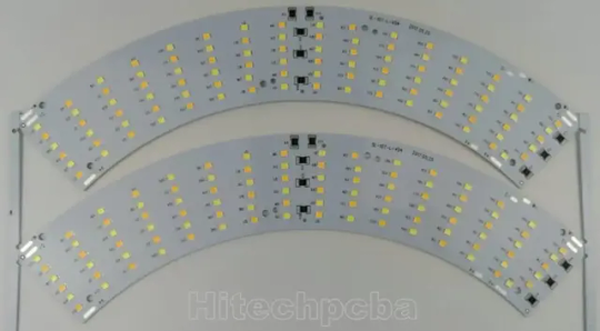
LED PCB Assembly
What is the LED Circuit Board assembly?
Generally, LED PCB assembly is considered to be a circuit board that has the LED components soldered to it. The LED is soldered to the printed circuit board and features a chip that creates the light as electrically connected. A thermal heat sink and a ceramic base are used to bond the chip. Not all the PCB products can be used in Led industry, as an LED PCB is easy to create a high volume of heat, but making it hard to cool with traditional methods. For this reason, metal core PCB is widely used in LED application because of their enhanced ability to dissipate heat, especially aluminum pcb is often used to fabricate PCB for LED lights.
We’ve had great LED PCB assembly experiences with top LED chips to brand such as Cree, Luxeon, Osram, Nichia, Lumileds, MLS, EVERLIGHT, Samsung, LG, Seoul., etc. PCB LED lights can be incorporated into numerous lighting applications due to their combination of excellent energy efficiency, low cost and maximum design flexibility.

Application of LED PCB Assembly
Hitechpcba serves customers in different industries, providing highly reliable and innovative LED PCBs for various applications:
• Horticulture light LED PCB Assembly
• LED controller PCB Assembly
• Computer LED display and indicators
• LED lights PCB Assembly for medical use
• Automotive LED PCBs Assembly include PCBs for brake lights and headlights
• Street lighting LED PCB Assembly
• Flashlights and camping accessories
• Traffic light PCB Assembly
• Commercial lighting LED PCB Assembly
LED PCB Assembly specification
Number of layers for LED PCB
These layers are made up of aluminum and magnesium, but now have Copper base material and Ceramic base materials for LED PCB industry, we can meet it.
Aluminum LED PCBs stand out among other PCBs because it has a good insulation characteristic and has a better machinery performance, the cheap cost is one important factor too.
Types of layers for LED PCB Assembly
Normally, the base layer is made using aluminum alloy metal.
This aluminum alloy substrate used in making the base makes it ideal for through-hole technology which transfers and dissipates heat.
A thermal insulation layer is made using some ceramic polymer which has good viscoelasticity characteristics.
It is highly heat resistant and protects the PCB against heat and mechanical stress.
The circuit layer, which is covered by a copper foil which can range from one to ten ounces.
LED Board type- single or in panel
Some boards are shapeless. For this reason, LED PCB panels are used. This reduces time, labor production and testing time.
Some LED PCB Assembly is done on a single board while others are done on panel boards.
LED PCB Assembly Process
Roughly, the PCBA process can be divided into theses phases: soldering paste printing > SMT (surface mounted technology) > reflow soldering > AOI (automated optical inspection)> THT (through-hole technology) > wave soldering > touch-up and cleaning > IC-programming > FCT (functional tests) > aging testing.
Below we show you the process.
Step1. Summarizing Project Information
Before contacting your supplier, make sure you have all the project information. Suppliers will need info following for quoting LED PCB assembly:
Gerber
BOM
LED PCB specification
Quotation quantity
Once you have gathered these information, you can contact us and request for a quote.
Of course, you can also provide the schematic, LED PCB Assembly pictures and even samples to us. The more details they have, the more accurate the supplier’s quotation will be.
Step2. Discussion and details about custom LED PCB Assembly
Different projects will have different requirements. Remember the special requirements mentioned in step 1? That’s going to be the focus of this session. Equipment and engineering capacity will not be identical between suppliers. Make sure your supplier has the equipment to produce and assemble major components and the corresponding testing capabilities.
For example, some vendors don’t have X-ray testing equipment, which means they can’t check the mount quality of BGA chips. Outsourcing this step will increase risk and cost. That’s what you don’t want.
Also, pay attention to time taken by the supplier to quote. Motherboards often contain hundreds or even thousands of components, and they are supplied by different manufacturers. To ensure the quality of the components, the supplier sourcing team will make multi-inquiries from these manufacturers or authorized suppliers to match customer’s requirement, which usually takes 2-3 business days, and even longer for some scarce chips. Therefore, if your project is complex and the supplier quotes you within few hours, double check with them.
Step3. Sample and feedback
After confirming the PI, the supplier will usually provide pre-production samples for your approval. At the same time, the supplier will also confirm with you the logistics plan of the bulk goods. Make sure they understand your shipping requirements, including details on packaging, customs clearance, taxes, etc.
For us to have a successful LED PCB Assembly process, its functions must be defined. Compliance requirement is defined to reduce the effect when components are selected.
The Bill of Materials is then generated from the information installed on the LED PCB.
All this information is used to assemble components which are identified from MOB to the LED PCB.
After that, the routing of traces is determined to each component, based on the size, shape of the circuit board and location of connectors.

Hitech Circuits is trusted by thousands of electronic engineers on their LED PCB assembly projects, from consumer, led bulb to precisely medical LED light, we can help you from the beginning of design stage; From commercial flood LED to industrial high power LED, from automotive LED to military LED, Venture is the perfect place for your LED PCB assembly requirement.
Hitech Circuits has been participated in hundreds and thousands of LED lighting projects, by providing LED PCB and also LED PCB assembly service.
Our LED PCB assembly had covered both ends of the Lighting Class LED size spectrum, assembling some of the largest (2 meter long boards) and some of the smallest LED Lighting applications which used in Medical Endoscopes.
LED PCB Assembly is very crucial in the current industrial development. Many electrical devises are being innovated and the old once being improved.
LED PCBs are useful due to the fact that they are made using materials that can transfer and dissipate heat. This characteristic increases device durability.
The world is changing with new technology, especially PCB technology that plays an essential role in the application of LED circuits. And the LED industry is taking advantage of this technology and growing faster.
As a full feature PCB solutions provider with more than a decade of experience, we're capable to provide LED PCB fabrication, components procurement and LED PCB assembly all under one roof. We can work with you to develop metal core PCB, aluminum circuit boards customized to your specific applications. We feature competitively priced PCBs made with standard FR-4 material that includes a thermal aluminum clad layer that will efficiently dissipate heat, keep all LED PCB components cool and significantly enhance the performance of your products.

LED pcb board, LED pcb assembly
LED with its advantages of high brightness, high efficiency, low heat, long life, is considered the most development potential in the 21st century lighting. In the market and policy driven by the rapid development of the domestic LED industry blowout has formed a relatively complete industrial chain, including the production of epitaxial wafers, chip preparation, packaging, integration, LED application. In 2010, China's LED industry scale, up from $ 827 billion in 2019 to 220 billion yuan, an annual growth rate of over 70%, higher than the 50% level of growth of the global LED lighting industry output value. Among them, the middle and lower reaches of the most complete industrial chain, accounting for 90% of the overall percentage of the GDP.Chinahas become the world's leading LED manufacturing base and important application market.
To further promote the technological innovation of the LED industry, construction and wide application of independent industry chain, China Electronic Appliance Corporation and industry associations to organize the theme of "Focus on the core energy LED Exhibition will be held November 9-11, 2010 in Shanghai International Expo Center and the 78th China Electronics Fair over the same period will be held will create from raw materials, epitaxial wafers, chip, LED bracket, LED accessories, LED packaging and supporting materials, the LED backlight upstream firm to the upstream and downstream enterprises of the display, lighting, landscaping, decorative lighting, traffic lights, automotive lighting, special lighting, to the equipment, instrumentation, software, finance, consulting and other service enterprises and technological exchanges and market trading platform, help the domestic industry sustained and healthy development, and promote the steady expansion of the LED application market.
In the LED industry chain upstream of the epitaxial wafers and LED chips accounted for 70% of the profits of the whole industry, and technology-intensive, capital-intensive, where the core technology of the LED. Well-known epitaxial wafer and chip production enterprises will be exhibited a number of energy-efficient, low heat, cost-effective LED products, many of whom have excellent products of international advanced level.
LED electronic pcb assembly��manufacturing 100% Original LED Chip with one-stop in-house pcba services
3 notes
·
View notes
Text
What is PCB Assembly ?
PCB Assembly manufacturer - Hitech Circuits Co., Limited
It’s the step in the manufacturing process in which you populate a blank board with the electronic components needed to make it into a functional printed circuit board. It’s these components that make a board into the circuit that enables an electronic product to function. PCB assembly typically takes place via one of two processes:
1. Surface-mount technology
SMT: SMT stands for “Surface Mount Technology“. The SMT components are very small sizes and comes in various packages like 0201, 0402, 0603, 1608 packages for resistors and capacitors. Similarly for Integrated circuits ICs we have SOIC, TSSOP, QFP and BGA.
The SMT components assembly is very difficult for human hands and can be time taking process so it is mostly done by automated pick and place machine.
2. Through-hole manufacturing
THT: THT stands for “Through hole Technology”. The components with leads and wires, like resistors, capacitors, inductors, PDIP ICs, transformers, transistors, IGBTs, MOSFETS are example.
The component has to be inserted on one side of PCB and pulled by leg on other side and cut the leg and solder it. The THT components assembly is usually done by hand soldering and is relatively easy.
Printed Circuit Board Assembly Techniques
There are only two common PCBA techniques available for use by a PCB designer. The methods are:
1. Automated PCB Assembly Techniques
Generally, this technique employs the use of state of the art machines, which are fully automatic. For example, the surface mount components are worth positioning with the aid of an automated pick and place machine.
Again, reflow soldering is commonly for surface mount components usually done in a reflow oven. An automated solder stencil is also used to apply the solder paste on the PCB.
Finally, high tech inspection machines are used to confirm and check the quality of the PCBA. Some of which include: Automated optical inspection machine (AOI), X-ray inspection machines, etc.
Above all, due to the precise monitoring, control of soldering, no human input and versatile machines.
This technique ensures utmost efficiency, output consistencies, and limits defects.
2. Manual PCB Assembly Techniques
This method is favorite for use with through-hole parts, which needs manual placement on the board. Besides, with these through-hole parts, it’s advisable you use wave soldering. Note that in the through- hole assembly process, you need to place the components and electronics on the PCB.
After that, you use wave soldering to solder the leads. Typically, you will need an individual to insert a component into a marked PTH. Once done, transfer the PCB to the next station where the next person will be on standby tasked with fixing another part.
What are the Benefits of SMT PCB Assembly?
SMT assembly provides many benefits and some of them are as follows:
It can be used to incorporate small components.
In SMT, the components can be placed on both sides of the board.
It assures high component densities.
Fewer holes need to be drilled for surface mounting than through-hole.
It require low initial costs and time for setting up the mass production.
SMT is the simpler and faster-automated assembly when compared to through-hole.
Errors regarding the component placement can be easily rectified.
Surface mount PCBs feature strong joints, which can easily withstand vibrations.
What are the techniques used in Surface Mount Technology?
There are several techniques for the reflow process. After applying the solder paste or a flux mixture on the board and after placing the components, the boards are conveyed to a reflow soldering oven. The techniques used for reflowing soldering include infrared lamps, hot gas convection, fluorocarbon liquids with a high boiling point, and so on.
What are the different testing methods used in SMT PCB Assembly?
Hitech Circuits as the PCB assembly manufacturer, we perform the following testing and inspection to ensure the quality of surface mount PCBs.
Automated Optical Inspection (AOI): This is performed before and after the soldering to identify the component placement, presence, and solder quality.
X-ray Testing: In this type of testing, the operator relies on the X-ray images of the PCB to check the solder joints and lead-less components such as Quad Flat Packs and ball grid arrays, which are generally not visible to naked eyes.
In-Circuit Testing (ICT): This method is used to detect manufacturing defects by testing the electrical properties in the SMT Assembly.
What type of files or documents should I send for SMT PCB Assembly?
Gerber Files: The file contains all details of physical board layers including solder masks, copper layers, drill data, legends, and so on.
Bill of Materials (BOM): This contains information on the list of items needed for the PCB manufacturing and the instructions of manufacturing.
Pick and Place File: This file contains information on all components to be used in the PCB design and their rotation and X-Y coordinates.
The whole process of PCB Assembly
1. Bare board loader machine
The first step in the PCB assembly is to arrange the bare boards on the rack, and the machine will automatically send the boards one by one into the SMT assembly line.
2. Printing solder paste
When PCB on the SMT production line, firstly, we have to print solder paste on it, and the solder paste will be printed on the pads of the PCB. These solder pastes will be melt and solder the electronic parts to the circuit board when it passes through the high-temperature reflow oven.
In addition, when testing new products, some people will use film board/adhesive cardboard instead of solder paste, which can increase the efficiency for adjusting the SMT machines.
3. Solder paste inspection machine(SPI)
Since the quality of solder paste printing is related to the quality of welding of subsequent parts, some SMT factories will use optical machine to check the quality of solder paste after printed the solder paste in order to ensure stable quality. If there any poorly printed solder paste board, we will wash off the solder paste on it and reprint, or remove the excess solder paste if there is redundant solder paste on it.
4. High speed SMT machine
Usually, we will put some small electronic parts (such as small resistors, capacitors, and inductors) to be printed on the circuit board first, and these parts will be slightly stuck by the solder paste just printed on the circuit board, so even if the speed of printing is very fast and the parts on the board will not fall away. But large parts are not suitable for use in such high speed SMT machines, which will slow down the speed of small parts assembly. And the parts will be shifted from the original position due to the rapid movement of the board.
5. Universal SMT machine
Universal SMT machine is also known as "slow machine", it will be assembled some large electronic components, such as BGA IC, connectors, etc., these parts need more accurate positions, so the alignment is very important. Use a camera to take a picture to confirm the position of the parts, so the speed is much slower than High speed SMT machine we taked before. Due to the size of the components here, not all of them are packed in tape and reel, and some may be packed in trays or tubes. But if you want the SMT machine to recognize the trays or tube-shaped packaging materials, you must configure an additional machine.
Generally, traditional SMT machines are using the principle of suction to move electronic parts, and in order to place the parts successfully, and there must be the flat surface on these electronic components for the suction nozzle of the SMT machine to absorb. However, for some electronic parts don’t have a flat surface for these machines, and it is necessary to order special nozzles for these special-shaped parts, or add a flat tape on the parts, or wear a flat cap for thees electronic parts.
6. Manual parts or visual inspection
After assembled all parts by the high speed SMT machine or Universal SMT machine and before going through the high-temperature reflow oven, and we will set up a visual inspection station here and to pick out the deviation parts or missing components boards etc., because we have to use a soldering iron to repair if there are still defectives boards after passing the high-temperature oven, which will affect the quality of the product and will also increase the cost. in addition, for some larger electronic parts or traditional DIP parts or some special reasons cannot be processed by the SMT machine before, they will be manually placed on pcb here.
7. Reflow oven
The purpose of reflow oven is to melt the solder paste and form a non-metallic compound on the component feet and the circuit board, that means to solder electronic components on the circuit board. The temperature rise and fall curves often affect the soldering quality of the entire circuit board. According to the characteristics of the solder materials, usually the reflow oven will set the preheating zone, soaking zone, reflow zone, and cooling zone to achieve the best soldering effect.
For example, the melting point for SAC305 solder paste with lead-free is about 217°C, which means that the temperature of the reflow oven must be higher than the melting points to remelt the solder paste. What's more, the maximum temperature in the reflow furnace should not exceed 250°C, otherwise many parts will be deformed or melted because they cannot withstand such a high temperature.
Basically, after the pcb passed through the reflow oven, the assembly for the entire circuit board is almost complete. If there are hand-soldered parts, we need to transfer to DIP process, and then we have to check the quality after reflow oven by QC department.
8. Automatic optical inspection(AOI)
The main purpose of setting up AOI is because some high density boards can’t be process the following ICT test, so we used AOI inspection to replace it. But even using AOI inspections, there still have the blind spots for such checking, for example, the solder pads under the components cannot be checked by AOI. At present, it can only check whether the parts have side standing issue, missing parts, displacement, polarity direction, solder bridges, lack of soldering etc., but cannot checking the BGA solderability, resistance value, capacitance value, inductance value and other components quality, so far AOI inspection can’t completely replace ICT test.
Therefore, there is still some risk if only AOI inspection is used to replace ICT testing, but ICT test is also not 100% make sure the good quality, we suggest these two ways can be combined with together to make sure the good quality.
9. PCB unloader machine
After the board is fully assembled, it will be retracted to the unloder machine, which has been designed to allow the SMT machine to automatically pick and place the board without damaging the quality for PCB.
10. Visual inspection for finished products
Normally there will be a visual inspection area in our SMT production line whether there is an AOI station or not, and it will help to check if there are any defectives after completed assembled the pcbs. If there is an AOI station, it can reduce the visual inspection worker on our SMT line, and to reduce the potential cost, and because it is still necessary to check some places that cannot be judged by AOI, many SMT factories will provide the mainly visual inspection templates at this station, which is convenient for visual inspection worker to inspect some key parts and polarity for components.
11. DIP process
DIP process is a very important process in the whole PCBA processing, and the processing quality will directly affect the functional for PCBA boards, so it is necessary to pay more attention to the DIP process. There are many preliminary preparations for DIP process. The basic process is to re-process the electronic components first, like to cut the extra pins for some DIP components, our staff received the components according to the BOM list, and will check whether the material part numbers and specifications are correct or not, and performs pre-production pre-processing according to the PCBA samples. The steps are: Use various related equipment (automatic capacitor pins cutting machine, jumper bending machine, diode and triode automatic forming machine, automatic belt forming machine and other machines) for processing.

12. ICT test
Printed Circuit board open/short circuit test (ICT, In-Circuit Test), The purpose of ICT test is mainly to test whether the components and circuits on the printed circuit board are open or short issues. It can also measure the basic characteristics of most components, such as resistance, capacitance, and inductance values to judge whether the functions of these parts are damaged, wrong parts or missing parts etc. after passing through the high-temperature reflow oven.
ICT test machines are divided into advanced and basic machines. The basic ICT test machines are generally called MDA (Manufacturing Defect Analyzer). It’s just to measure the basic characteristics of electronic components and judge open and short circuits issue we talked above.
In addition to all the functions of the basic ICT test machines, for advanced ICT test machine can also test the whole PCBA by using power, start to testing the PCBA boards by setting the program in the test machine. The advantage is that it can simulate the function of the printed circuit board under the actual power-on condition, this test can partly replace the following functional test machine (Function Test). But the cost for the test fixture of this advanced ICT test can probably buy a car, it’s too expensive and we suggest it can be used in mass production products.
13. PCBA function test
Functional testing is to make up for the ICT test, because ICT only tests the open and short circuits on the the PCBA board, and other functions such as BGA and other fuctions are not tested, so it is necessary to use a functional testing machine to test all functions on the whole PCBA board.
14. Cutting board (assembly board de-panel)
Normally, printed circuit boards will be produced in panel, and it will be assembled to increase the efficiency of SMT production. It means several single boards in one panel, such as two-in-one, four-in-one etc. After finished all the pcb assembly process, it needs to be cut into single boards, and for some printed circuit boards with only single boards also need to cut off some redundant board edges.
There are several ways to cut the printed circuit board. You can design the V-cut using the blade cutting machine (Scoring) or directly manually break off the board (not recommended). For more high density circuit boards, it will be used the professional splitting machine or the router to split the board without any damage the electronic components and printed circuit boards, but the cost and working hours will be a little longer.
Why Choose Hitech Circuits PCB Assembly Manufacturer for Your PCB Assembly Projects?
There are several PCB manufacturers specializing in PCB assemblyservices. However, Hitech Circuits PCB Assembly stands out owing to the following:
Assistance in Material Procurement:
Technically, in PCB assembly services, the quality of parts is the responsibility of the OEM; however, we ease your job by assisting you to make the right selection. We can help you procure all your parts of the same type own a single part number, thanks to our supply chain and vendor network as well as experience. This saves time and cost that goes in ordering single parts as you plan.
Testing procedures:
We are very focused on quality and thus implement stringent testing procedures at each stage of the assembly and after completion.
Fast Turnaround Times:
Our well-equipped facility and the right tools enable us to complete your requirements well before time, and without compromising on the quality or functioning of the PCBs. For simple designs we revert in 24 to 48 hours.
Cost Effectiveness:
While PCB assembly is a cost-effective alternative, we go a step further and assure that the parts you list are of a good quality and suitable for your requirement. Also, you can control the part flow and replenish them as needed. This eliminates the need to buy extra stock and store it.
Quick Quote:
We offer a quick quote based on your BOM. All you need is a detailed BOM, Gerber files, your application requirement sheet, and quantity.
We’re not one to stand still, which is why we use the latest equipment and the finest minds to create your PCB projects. We’re constantly keeping our finger on the pulse of the latest trends. And as a result, we know how to deliver the highest standards of PCB assembly to meet all your requirements.
Our dedicated, friendly customer service team also means that we support you every step of the way. Offering our expert guidance to ensure a complete PCB project that you’re happy with.
Contact us today
No matter what your printed circuit board assemblyneeds are, we always aim to deliver efficient, dependable solutions. For more information about our services, do not hesitate to get in touch with us today for a no-obligation quote
2 notes
·
View notes
Text
Aimtron: Your Reliable Partner for PCB Assembly Manufacturing Services in Illinois

In the fast-paced world of electronics manufacturing, having a trusted partner for PCB assembly services can make all the difference. That’s where Aimtron Corporation stands out. Located in the heart of Illinois, Aimtron has established itself as a leader in providing end-to-end PCB assembly and electronics manufacturing services to clients across a wide range of industries—from aerospace and defense to healthcare, industrial automation, and consumer electronics.
Why Choose Aimtron?
1. Comprehensive PCB Assembly Services
Aimtron offers a full spectrum of PCB assembly services including:
Surface Mount Technology (SMT)
Through-Hole Assembly
Turnkey PCB Assembly
BGA and Micro-BGA Assembly
Prototyping to Full-Scale Production
Whether you need a quick-turn prototype or high-volume production, Aimtron has the technology and expertise to deliver consistent quality.
2. State-of-the-Art Manufacturing Facility
At Aimtron’s Illinois facility, quality is more than a promise—it’s a standard. Equipped with cutting-edge SMT lines, automated optical inspection (AOI), X-ray inspection for BGAs, and in-circuit testing, Aimtron ensures every board meets the highest quality benchmarks.
3. Engineering Excellence
Aimtron doesn’t just assemble PCBs; it partners with clients from concept to production. Their team of skilled engineers provides:
Design for Manufacturability (DFM)
Design for Testability (DFT)
Component sourcing and BOM optimization
Technical support and value engineering
This collaborative approach reduces lead times, lowers costs, and enhances product reliability.
4. Commitment to Quality and Compliance
Aimtron is ISO 9001 and ISO 13485 certified, ITAR registered, and RoHS compliant, ensuring adherence to global quality and regulatory standards. Their robust quality management system supports continuous improvement and customer satisfaction.
5. Customer-Centric Approach
Aimtron believes in building long-term partnerships. Their customer-first philosophy translates into responsive communication, transparent pricing, and a flexible manufacturing model that adapts to changing project needs.
Serving Illinois and Beyond
While Aimtron proudly operates from Illinois, its reputation for reliability and precision extends far beyond state lines. Clients across the U.S. and internationally trust Aimtron for mission-critical electronics manufacturing solutions delivered on time and within budget.
Industries Served
Medical Devices
Aerospace & Defense
Automotive
Industrial Control
Consumer Electronics
IoT & Smart Devices
Let’s Build the Future Together
At Aimtron, innovation meets execution. With a perfect blend of technology, talent, and tenacity, Aimtron is not just a PCB assembly vendor—it’s your strategic partner in bringing great ideas to life.
Looking for a dependable PCB assembly manufacturer in Illinois? Partner with Aimtron and experience quality, reliability, and excellence every step of the way.
#ElectronicsManufacturing#PCBAssemblyServices#DesignforTestability#DesignforManufacturability#PCBassemblymanufacturerinIllinois#SurfaceMountTechnology#Through-HoleAssembly
0 notes
Text
High-Performance Thermally Conductive Adhesives – First Seal India
As electronics and industrial systems grow more compact and powerful, efficient heat dissipation becomes critical. One essential solution in thermal management is the use of thermally conductive adhesives. First Seal India stands out as a trusted supplier in India, delivering high-performance thermal adhesive solutions that offer both strong mechanical bonding and superior heat transfer capabilities.
What Are Thermally Conductive Adhesives?
Thermally conductive adhesives are specially formulated compounds designed to bond components while facilitating the transfer of heat away from sensitive electronics or mechanical parts. They are commonly used in LED lighting, power electronics, automotive systems, and heat sinks.
Why Choose First Seal India?
At First Seal India, we understand the balance between thermal conductivity, structural strength, and electrical insulation. Our thermally conductive adhesives are manufactured to meet the needs of cutting-edge industries requiring precise heat management and long-term reliability.
Key Product Features:
High Thermal Conductivity: Efficient heat dissipation (typically 1.0 – 6.0 W/mK)
Excellent Bond Strength: Long-lasting adhesion to metals, ceramics, and plastics
Dielectric Properties: Safe for use around sensitive electronic circuits
Chemical and Moisture Resistance: Performs in harsh environmental conditions
Customization Options: Available in one-part or two-part formulations (epoxy, silicone)
Applications:
Our thermally conductive adhesives are used in:
Heat sinks and power modules
Battery packs and EV components
LED assemblies and PCB bonding
Consumer electronics and telecom equipment
Industrial automation and HVAC units
Trusted by Engineers, Preferred by Industries
Backed by years of expertise in sealing, bonding, and adhesive technologies, First Seal India provides solutions that combine performance, durability, and application ease. We also offer technical support and formulation customization based on your industry requirements.
Explore our full range of adhesive and thermal management products at: 👉 https://firstsealindia.com/
0 notes
Text
Printed Circuit Board Assembly For Small And Large Orders
Printed Circuit Board Assembly (PCBA) is the system of mounting digital components onto a PCB. It involves soldering, placement, and inspection. PCBA is crucial in production electronics like smartphones, computer systems, and clinical devices. Quality manipulation, precision, and automation are key factors in making sure a dependable and useful meeting.
0 notes
Text
SMT Meaning: Understanding Surface-Mount Technology in Modern Electronics
Introduction
As technology continues to evolve, SMT (Surface-Mount Technology) has become the preferred method for assembling electronic devices. SMT enables the direct placement of components onto printed circuit boards (PCBs), allowing manufacturers to create compact, efficient, and high-performance electronics. This article explores the meaning of SMT, its benefits, applications, and future trends.
What is SMT meaning?
Surface-Mount Technology (SMT) is an electronics manufacturing technique where components are mounted directly onto the PCB surface rather than inserted into pre-drilled holes. This method enhances efficiency, reduces material usage, and streamlines automated production.
How SMT Works
1. Solder Paste Application
A layer of solder paste is precisely applied to areas on the PCB where components will be placed.
2. Automated Component Placement
Advanced pick-and-place machines position electronic components onto the board with precision.
3. Reflow Soldering
The PCB passes through a controlled heating process, melting the solder paste and forming secure electrical connections.
4. Inspection & Testing
Automated and manual inspections ensure component placement accuracy and functionality.
Key Advantages of SMT
1. Miniaturization
Allows for high-density circuit designs, reducing device size and weight.
2. Faster Production
Automation speeds up assembly, improving manufacturing efficiency.
3. Enhanced Electrical Performance
Shorter pathways improve conductivity and signal reliability.
4. Cost Savings
Reduces material consumption and lowers manufacturing costs.
5. Compatibility with Advanced Components
Supports microprocessors, wireless communication modules, and high-speed circuits.
Applications of SMT Technology
1. Consumer Electronics
Smartphones, tablets, and gaming consoles rely on SMT for efficient and compact circuitry.
2. Automotive Electronics
SMT is used in vehicle control units, infotainment systems, and safety sensors.
3. Medical Devices
Precision diagnostic tools, portable monitoring systems, and wearable health technology benefit from SMT.
4. Industrial Automation
Robotics, control systems, and IoT-enabled sensors are optimized with SMT components.
5. Aerospace and Defense
High-reliability circuit designs in satellites, avionics, and military-grade electronics use SMT technology.
Future of SMT Technology
Several advancements continue to shape SMT manufacturing, including:
Flexible PCBs – Supporting curved and bendable circuits for next-generation devices.
AI-Assisted Assembly – Improving automation precision and reducing defects.
Miniaturization Innovations – Shrinking components for even more compact designs.
Conclusion
SMT technology has revolutionized electronics manufacturing, enabling high-performance, compact, and cost-effective device production. As demand grows for smaller, smarter, and more powerful electronics, SMT will remain a critical factor in shaping the future of technology.
0 notes
Text
PCB Manufacturing: A Comprehensive Guide to Printed Circuit Board Production

Introduction to PCB Manufacturing
PCB manufacturing is the process of creating printed circuit boards, which are essential components in nearly all modern electronic devices. From smartphones to industrial machinery, PCBs provide the foundation for electrical connections and component mounting. This guide explores the PCB manufacturing process, materials, technologies, and applications.
The PCB Manufacturing Process
1. Design and Schematic Creation
Before production begins, engineers design the PCB using specialized software like Altium Designer, KiCad, or Eagle. The design includes:
Schematic diagrams (circuit connections)
Component placement
Trace routing (copper pathways)
Layer stack-up (for multi-layer PCBs)
Once the design is finalized, a Gerber file (standard PCB manufacturing file) is generated for fabrication.
2. Material Selection
The base material of a PCB is typically FR-4, a flame-resistant fiberglass epoxy laminate. Other materials include:
Flexible PCBs: Made from polyimide for bendable circuits.
High-frequency PCBs: Use Rogers material for RF applications.
Metal-core PCBs: Aluminum or copper for heat dissipation.
3. Printing the Circuit Pattern
The PCB design is transferred onto the board using one of these methods:
Photolithography: A UV-sensitive photoresist is applied, exposed to UV light, and developed to create the circuit pattern.
Direct Imaging: A laser directly etches the pattern onto the PCB.
4. Etching the Copper Layers
After the circuit pattern is printed, the unwanted copper is removed through chemical etching. The remaining copper forms the conductive traces.
5. Drilling Holes for Components
Precision CNC machines drill holes for through-hole components and vias (connections between layers).
6. Plating and Copper Deposition
The drilled holes are electroplated with copper to ensure conductivity between layers.
7. Solder Mask Application
A solder mask (usually green) is applied to protect the copper traces and prevent short circuits. Openings are left for soldering components.
8. Silkscreen Printing
Text, logos, and component labels are printed on the PCB using silkscreen ink for easy assembly and identification.
9. Surface Finish Application
A surface finish is applied to protect exposed copper and improve solderability. Common finishes include:
HASL (Hot Air Solder Leveling)
ENIG (Electroless Nickel Immersion Gold)
OSP (Organic Solderability Preservative)
10. Electrical Testing and Quality Control
Each PCB undergoes automated optical inspection (AOI) and electrical testing to ensure functionality. Defective boards are rejected.
Types of PCBs in Manufacturing
1. Single-Layer PCBs
Simplest and most cost-effective.
Used in basic electronics like calculators.
2. Double-Layer PCBs
Conductors on both sides.
Common in consumer electronics.
3. Multi-Layer PCBs
4+ layers for complex circuits (e.g., motherboards).
Requires precise PCB manufacturing techniques.
4. Flexible PCBs
Used in wearables and medical devices.
Made from bendable materials.
5. Rigid-Flex PCBs
Combines rigid and flexible sections.
Ideal for aerospace and military applications.
Advanced PCB Manufacturing Technologies
1. High-Density Interconnect (HDI) PCBs
Features microvias and finer traces.
Used in smartphones and compact devices.
2. Embedded Components
Passive components (resistors, capacitors) are embedded within the PCB.
Reduces size and improves performance.
3. 3D Printed Electronics
Emerging technology for rapid prototyping.
Combines additive manufacturing with conductive inks.
Applications of PCB Manufacturing
PCBs are used in nearly every industry, including:
Consumer Electronics (Smartphones, Laptops)
Automotive (ECUs, Infotainment Systems)
Medical Devices (Pacemakers, Imaging Systems)
Aerospace & Defense (Avionics, Radar Systems)
Industrial Automation (Robotics, Control Systems)
Challenges in PCB Manufacturing
Miniaturization: Shrinking component sizes demand precision.
High-Speed Signal Integrity: Ensuring minimal interference.
Thermal Management: Preventing overheating in dense circuits.
Environmental Regulations: Compliance with RoHS and REACH.
Future Trends in PCB Manufacturing
AI-Driven Design Optimization
Sustainable Materials (Biodegradable PCBs)
5G and IoT Integration (Higher frequency PCBs)
Automated Smart Factories (Industry 4.0)
Conclusion
PCB manufacturing is a complex yet vital process that powers modern electronics. From design to testing, each step requires precision and expertise. As technology advances, printed circuit boards will continue to evolve, enabling smaller, faster, and more efficient devices.
Whether you're an engineer, hobbyist, or industry professional, understanding PCB manufacturing helps in designing better electronic products for the future.
1 note
·
View note
Text
Top 5 Mistakes OEMs Make When Ordering ICT Fixtures
Imagine this: you're holding a sleek new smartphone, a cutting-edge medical device, or a car key fob that effortlessly connects to a smart vehicle. Behind the scenes, these modern marvels owe their flawless function to a critical yet often overlooked piece of engineering: the ICT Fixture.
In the world of electronics manufacturing, even the tiniest defect can lead to costly recalls, product failures, or customer dissatisfaction. That’s why In-Circuit Testing (ICT) remains a gold standard for ensuring quality and reliability. But for ICT to do its job effectively, it needs a sidekick built for precision and performance—the ICT Fixture.
Whether you're an OEM, a test engineer, or just curious about how complex circuit boards pass the quality test, this article breaks down why ICT Fixtures are the quiet heroes behind electronics you trust every day—and how they can transform your testing process from good to great.
Understanding the Basics: What is an ICT Fixture?
An ICT Fixture, short for In-Circuit Test Fixture, is a specialized mechanical tool used during the In-Circuit Testing (ICT) process. It connects the PCB to the test equipment using a bed-of-nails configuration, where spring-loaded test probes make contact with specific test points on the board.
These fixtures are engineered to precisely align with a given PCB layout. Once the board is placed on the fixture and clamped down, the ICT system runs a comprehensive battery of tests, verifying resistors, capacitors, transistors, diodes, solder joints, and even integrated circuits.
ICT Fixtures are essential in catching production faults such as:
Solder bridges
Missing or misaligned components
Open circuits
Incorrect component values
In high-volume manufacturing, the ICT Fixture becomes a gatekeeper of quality, ensuring that defective boards are identified and corrected before final assembly.
Why ICT Fixtures Still Matter in an Evolving Industry
With the rise of surface mount technology (SMT), miniaturization, and increasingly complex multilayer PCBs, some manufacturers have shifted towards automated optical inspection (AOI) or boundary-scan testing. But ICT Fixtures continue to offer advantages that are difficult to replace:
Comprehensive Component-Level Testing: ICT can test passive and active components under power conditions—something AOI or X-ray inspection can't provide.
Speed and Efficiency: For high-volume assembly lines, ICT Fixtures reduce testing time dramatically. Once the fixture is built, each board can be tested in seconds.
Repeatability and Accuracy: With well-designed fixtures, testing results are reliable and repeatable across thousands of units.
Integration with Functional Testing: Many manufacturers are now integrating ICT with functional test stations for a holistic quality assurance approach.
Custom ICT Fixtures: Precision is Everything
One-size-fits-all doesn't apply in the world of ICT Fixtures. Each fixture must be customized to the unique layout of a PCB. This means close collaboration between fixture manufacturers and the client’s engineering teams.
From choosing the right probe types to designing ergonomic enclosures, every detail matters. High-end fixture designers also provide value-added features such as:
Vacuum hold-down mechanisms
Pneumatic clamping systems
Guided probe modules for high-density test areas
ESD-safe materials
Easy-change fixtures for multi-product testing
If you're looking for a partner that combines cutting-edge fixture design with proven reliability, Equip-Test offers a range of ICT Fixtures tailored for various industries—from automotive and telecommunications to consumer electronics and medical devices.
Choosing the Right ICT Fixture Partner
When selecting a provider for your ICT Fixture needs, consider the following factors:
Experience and Industry Knowledge: A provider familiar with your specific sector will anticipate layout challenges and compliance requirements.
Customization Capability: Each board is different. Your partner should offer 100% custom fixture builds based on your PCB Gerber files and test requirements.
Support for Test Program Development: Some fixture companies also offer ICT test programming, which helps reduce your internal workload and ensures compatibility from the get-go.
Turnaround Time: In fast-moving production environments, lead time matters. Look for suppliers that can deliver quality fixtures quickly without sacrificing precision.
Equip-Test stands out in this space, offering not only custom ICT Fixtures but also full support for test programming, fixture repair, and upgrades, ensuring long-term value for your investment. Learn more here: https://bit.ly/3RfmPhU
Final Thoughts: ICT Fixtures Keep Your Production Flowing
In a world obsessed with innovation and rapid product cycles, it's easy to overlook the critical role of quality control. But make no mistake—without robust ICT Fixtures, the risk of faulty electronics slipping into the market rises sharply.
By investing in high-quality ICT Fixtures and partnering with experts who understand your testing challenges, you’re building a manufacturing process that’s not only fast and efficient but also trusted.
If you're ready to elevate your testing capabilities and improve PCB validation, consider working with a seasoned team like Equip-Test. Precision matters—and so does your reputation.
0 notes
Text
Finding the Right PCB Fabrication and Assembly Company in India: Powering the Future of Electronics
In the fast-paced world of electronics, every component matters—especially the printed circuit board (PCB). It’s the backbone of every electronic device, from smartphones and smartwatches to industrial machines and medical instruments. That’s why selecting a reliable PCB fabrication company in India or a trusted PCB assembly company in India is a critical step for businesses aiming to produce high-quality products efficiently and cost-effectively.

At FindingMFG, we understand how important it is to find the right manufacturing partner. Our platform bridges the gap between global buyers and India’s top electronics manufacturers, streamlining the sourcing process and ensuring reliability every step of the way.
Why Choose a PCB Fabrication Company in India?
India has positioned itself as a global electronics manufacturing hub, with a rapidly growing ecosystem of PCB fabricators offering cutting-edge technology, competitive pricing, and fast delivery. Many Indian manufacturers now operate with fully automated plants, IPC standards compliance, and global certifications such as ISO 9001 and RoHS.
Here’s why India is an ideal destination for PCB fabrication:
Advanced Capabilities: From single-layer prototypes to complex multi-layer PCBs and HDI boards, Indian companies deliver precision and performance.
Cost Advantage: Get world-class quality at a fraction of the cost compared to Western markets.
Faster Turnaround: Indian manufacturers are known for agile production cycles and on-time delivery.
Custom Solutions: Whether you need rigid, flex, or metal-core PCBs, customization is readily available.
By choosing the right PCB fabrication company in India, companies can reduce lead times, optimize costs, and ensure product reliability.
What Makes a Great PCB Assembly Company in India?
While PCB fabrication builds the board, PCB assembly brings it to life. A top-notch PCB assembly company in India offers end-to-end assembly services, ensuring that every component is placed and soldered with accuracy.
Here are key features to look for:
Full-Service Assembly: Including SMT (Surface Mount Technology), THT (Through-Hole Technology), and mixed assembly.
Component Sourcing: Reliable partners work with authorized distributors to ensure component authenticity.
Quality Control: Automated Optical Inspection (AOI), X-ray inspection, and functional testing reduce the risk of defects.
Box Build Capability: For clients looking for complete product assembly and packaging services.
Partnering with a skilled PCB assembly provider ensures that your final product meets both performance and durability standards.
Why Use FindingMFG?
FindingMFG is more than just a sourcing platform. We simplify your search for a dependable PCB fabrication company in India or PCB assembly company in India by providing:
🌐 A curated list of verified and certified manufacturers
🔍 Instant quote comparison and transparent pricing
🚚 Support for low-volume prototyping to high-volume production
🤝 Global buyer-supplier matchmaking with seamless communication tools
Whether you’re an electronics startup prototyping your first board or an established OEM looking to scale, FindingMFG ensures you connect with the right partners, faster and smarter.
Final Thoughts
As the demand for electronics grows, the need for dependable manufacturing partners becomes essential. Choosing the right PCB fabrication and PCB assembly company in India can make all the difference in your product’s quality, time-to-market, and overall success.
With FindingMFG, you gain access to India’s best electronics manufacturing resources—all in one place. Start your sourcing journey with confidence today
#pcb fabrication company#pcb fabrication company in india#pcb assembly company in india#pcb design#pcb manufacturing company#electronics manufacturing company
0 notes
Text
PCB Manufacturing: A Comprehensive Guide to Printed Circuit Board Production

Introduction to PCB Manufacturing
PCB Manufacturing is the process of creating Printed Circuit Boards (PCBs), which are essential components in nearly all modern electronic devices. From smartphones to industrial machinery, PCBs provide the foundation for electrical connections, enabling devices to function efficiently. This guide explores the PCB Manufacturing process, materials used, key technologies, and industry trends.
The PCB Manufacturing Process: Step by Step
The production of Printed Circuit Boards involves multiple stages, each requiring precision and expertise. Below is a detailed breakdown of the PCB Manufacturing workflow.
1. Design and Schematic Creation
Before production begins, engineers design the PCB using specialized software like Altium Designer, Eagle, or KiCad. The schematic defines the electrical connections, while the layout determines the physical placement of components.
2. Printing the PCB Design
Once the design is finalized, it is printed onto a laminate material using a photoplotter, which transfers the circuit pattern onto a film.
3. Substrate Preparation
The base material, typically FR-4 (fiberglass-reinforced epoxy laminate), is cleaned and coated with a photosensitive layer called photoresist.
4. Exposure and Developing
The photoresist-coated substrate is exposed to UV light through the printed film. The exposed areas harden, while the unexposed regions are washed away during the developing stage.
5. Etching the Copper Layers
The board is then immersed in an etching solution (usually ferric chloride or ammonium persulfate), which removes unwanted copper, leaving only the desired circuit traces.
6. Drilling Holes for Components
Precision CNC machines drill holes for through-hole components and vias (electrical connections between layers).
7. Plating and Copper Deposition
A thin layer of copper is electroplated onto the board to strengthen the connections and ensure conductivity.
8. Solder Mask Application
A solder mask (usually green, but available in other colors) is applied to protect the copper traces from oxidation and prevent solder bridges.
9. Silkscreen Printing
Component labels, logos, and reference indicators are printed onto the board using silkscreen printing for easier assembly.
10. Surface Finish Application
To prevent oxidation and improve solderability, a surface finish (such as HASL, ENIG, or OSP) is applied.
11. Electrical Testing and Quality Control
Automated AOI (Automated Optical Inspection) and flying probe testers verify electrical connectivity and detect defects.
12. Final Assembly and Shipping
Once tested, the PCBs are assembled with components (if required) and shipped to manufacturers for integration into electronic devices.
Materials Used in PCB Manufacturing
The quality of a Printed Circuit Board depends heavily on the materials used. Key materials include:
Copper Foil: Conducts electricity and forms the circuit traces.
FR-4 Substrate: Provides mechanical strength and insulation.
Solder Mask: Protects copper traces and prevents short circuits.
Silkscreen Ink: Adds labels and markings for assembly.
Surface Finishes (HASL, ENIG, OSP): Enhances solderability and durability.
Advanced PCB Manufacturing Technologies
As electronics evolve, PCB Manufacturing techniques continue to advance. Some cutting-edge technologies include:
1. High-Density Interconnect (HDI) PCBs
These boards feature microvias, finer traces, and multiple layers, enabling compact designs for smartphones and wearables.
2. Flexible and Rigid-Flex PCBs
Made from polyimide or other flexible materials, these PCBs are used in bendable electronics like foldable phones and medical devices.
3. Multilayer PCBs
With 4 to 50+ layers, these PCBs are essential for complex devices like servers and aerospace systems.
4. Embedded Components
Passive components (resistors, capacitors) are embedded within the PCB, reducing size and improving performance.
5. 3D Printed Electronics
Additive manufacturing is being explored for rapid PCB prototyping, allowing faster design iterations.
Challenges in PCB Manufacturing
Despite advancements, PCB Manufacturing faces several challenges:
Miniaturization: As devices shrink, producing ultra-fine traces becomes difficult.
Signal Integrity: High-speed circuits require precise impedance control.
Thermal Management: Dense PCBs generate heat, necessitating effective cooling solutions.
Environmental Regulations: Restrictions on hazardous materials (lead, halogen) impact manufacturing processes.
Future Trends in PCB Manufacturing
The PCB Manufacturing industry is evolving with new trends:
AI and Automation: Machine learning improves defect detection and process optimization.
Sustainable Manufacturing: Eco-friendly materials and lead-free soldering gain traction.
5G and IoT Demand: High-frequency PCBs are needed for 5G networks and IoT devices.
Additive Manufacturing: 3D printing could revolutionize prototyping and low-volume production.
Conclusion
PCB Manufacturing is a complex yet vital industry that powers modern electronics. From design to final testing, each step requires precision to ensure reliability and performance. As technology advances, Printed Circuit Boards will continue to evolve, enabling smaller, faster, and more efficient electronic devices. Understanding the PCB Manufacturing process helps engineers, designers, and manufacturers stay ahead in this rapidly changing field.
By keeping up with emerging trends and overcoming challenges, the PCB Manufacturing industry will remain at the heart of technological innovation. Whether for consumer electronics, automotive systems, or aerospace applications, high-quality PCBs are indispensable in today’s connected world.
1 note
·
View note
Text
Open source 24-channel USB high-voltage driver
When it comes to automation and control systems, there's often a need for multiple digitally controlled output terminals with high-voltage handling capabilities. Many existing modules are bulky, expensive, or require numerous additional components to function. To address this gap, I've developed a fully open-source, USB-controlled 24-channel high-voltage driver. This device provides precise, flexible control in a compact and user-friendly package. The project is open hardware, released under the CERN-OHL-W license, ensuring transparency from hardware schematics to firmware code. The driver module communicates via USB using a simple virtual COM port, eliminating the need for special drivers and complex setups.

At the core of the system are three TPIC6B595 shift registers, each supplying eight open-drain outputs that can handle up to 50V and sink currents of up to 150mA per channel. These registers are daisy-chained to achieve a total of 24 outputs. The outputs are designed for low-side switching and include integrated clamping diodes, making them suitable for driving inductive loads such as relays and solenoids. Data is clocked into the registers through serial input from a microcontroller, allowing for fast and reliable state updates across all channels with just a few lines of code.
The logic and communication for this module are managed by the STC15W204S microcontroller, a cost-effective yet powerful 8051-based MCU with enhanced UART performance and an integrated oscillator. This chip is paired with a CH340N USB-to-UART bridge, which presents the device as a standard virtual COM port to the host PC. Upon connection, the microcontroller listens for a set of AT-style commands sent over the serial connection. These commands are straightforward and user-friendly, for example, "ON=65280" activates the middle 8 outputs, "CLR" turns off all channels, and "VER" retrieves the firmware version. Additionally, there is a command to save the current output state to the built-in EEPROM, enabling the system to restore its output to a known state after power cycles. This interface design is perfect for scripting, automation, or integration with software tools such as Python, LabVIEW, or custom control GUIs.
The PCB is designed using KiCad and features a 2-layer layout measuring 75.25mm × 33.75mm. It includes 2.54mm pitch headers for output connections and is equipped with a USB Type-C connector. Power can be supplied through either USB or an external regulated 5V source, which can be selected via onboard jumper settings. The layout ensures clean signal routing and minimizes crosstalk or interference, even when switching high-voltage loads. Careful decoupling and protection components provide robustness for real-world applications.

The PCB for this module was fabricated by PCBWay, who generously sponsored this project. PCBWay offers high-quality PCB manufacturing and assembling services. Also, they offer CNC and 3D printing services. The PCB of this module is available to order from PCBWay. Check out the PCBWay website for its manufacturing capabilities and pricing.
The firmware for the STC15W204S is written in C using SDCC. It is easy to expand the command set, introduce new communication modes, or add timed control logic as needed. The current implementation allows full 24-bit output control using a base 10 numerical mask, making it both scriptable and human-readable. Thanks to the preloaded bootloader of the STC15W204S, firmware updates can be performed through the same serial interface. Details about this process are covered in the project documentation. Like the hardware, the firmware is released under the MIT License and is available in the project repository.
The system has been tested with a variety of 12V and 24V inductive and resistive loads, including relay banks, solenoids, and LED arrays. Since the outputs are open-drain, external voltages up to 50V can be safely switched on each channel making it ideal for a range of industrial, laboratory, or artistic applications. Output timing is reliable, with clean edge transitions observed during scope testing, and no signal integrity issues even during full 24-channel toggling. It is recommended to use individual heatsinks for the driver ICs when driving high-current inductive loads with this module. While the printed circuit board has heat transfer traces, the addition of individual heatsinks can increase the durability of the module.

Potential use cases for this module include automated test benches, home automation systems, signal routing for instrumentation, nixie tube multiplexing, and other high-voltage control tasks. The command-based protocol makes it easy to script operations or integrate this module into a larger system.
For those who wish to explore the schematics, command protocol, design rationale, and usage examples in greater depth, I have published comprehensive documentation and resources in the project wiki. This includes detailed assembly instructions, firmware flashing guidance, and tips on customizing the firmware for enhanced functionality.
All source files - including schematics, PCB layout, firmware code, and the bill of materials - are freely available at https://github.com/dilshan/24ch-usb-high-voltage-driver.
0 notes
Text
Electronics Manufacturing Services
Iljin is a leading provider of Electronics Manufacturing Services (EMS), offering end-to-end solutions including PCB assembly, prototyping, turnkey manufacturing, and quality testing. With advanced technology, a global supply chain, and strict quality control, Iljin serves industries like automotive, consumer electronics, medical devices, and industrial automation. Our commitment to innovation, precision, and reliability ensures efficient production and faster time-to-market for your products. Partner with Iljin to streamline your manufacturing process and achieve superior performance with every build. Trusted globally for excellence in electronics manufacturing.
0 notes
Text
DAEJOO : A Trusted Name in Marine & Industrial Automation Explore the Full Range at Aeliya Marine
In the constantly changing world of ocean and industrial automation, few names have withstood the test of time, providing precision, reliability, and confidence. One of them is DAEJOO, known around the globe for its cutting-edge engineering and high-reliability parts. Be it a business vessel traveling open seas or an assembly line that cannot pay the luxury of a second of downtime, DAEJOO’s automation components guarantee performance sans compromise.
At Aeliya Marine Tech, we are pleased to showcase a handpicked range of original DAEJOO products designed to satisfy marine engineers as well as industrial specialists. Ranging from hard-to-find PCBs to reliable relay units and control modules, our DAEJOO product portfolio is extensive, quality-approved, and ready to ship across the globe.
About DAEJOO Engineering Excellence You Can Rely On
DAEJOO Industrial Co., Ltd., based in South Korea, is a renowned producer of marine-grade electrical and automation components. With an emphasis on high-performance circuit design, interface reliability, and system safety, DAEJOO has emerged as the go-to option for shipyards, offshore platforms, naval maintenance teams, and industrial control engineers globally.
The mission of the company has ever been simple: to produce parts that endure, even in extreme environments. Those are products resistant to high humidity, saltwater corrosion, voltage spikes, and temperature extremes conditions prevalent both in marine and heavy industrial applications.
Discover the DAEJOO Product Categories at Aeliya Marine
Let’s start with some of the fundamental product categories found on our website under the DAEJOO banner:
1. Control Modules
DAEJOO’s control modules are the workhorse of a wide range of shipboard and industrial automation applications. With sturdy build quality and reliable interfacing logic, the modules provide the seamless execution of commands and control signals on any automation network.
Standard features :
High insulation resistance
DIN-rail mounting with compact dimensions
LED indication of diagnostic status
Fail-safe options
2. Interface Boards & PCBs
DAEJOO Printed Circuit Boards (PCBs) are designed to provide precise signal control and voltage regulation. They find application in main control panels, sensor systems, navigation controls, and motor interface units.
Regardless of whether you’re replacing a defective board or modernizing an old system, these PCBs provide :
Consistent copper trace paths
Built-in EMI protection
Components with surface-mount or through-hole
Clear part labeling and revision control
3. Relays & Timer Units
DAEJOO relays are ideal for timed switching, fault detection, and manual override systems applications. Their small sizes and conventional pin configurations simplify integration.
Benefits are:
Low power coil operation
Long mechanical and electrical life
High surge withstand capacity
ISO and IEC compliance
4. Power Supply Units & I/O Modules
In both factory and marine systems, power stability and input/output control are essential. DAEJOO’s power supply units provide stable voltage output with protective features such as overcurrent and thermal shutdown.
At the same time, their I/O modules provide :
Modular expansion
Easy plug-and-play connections
Flexible voltage and signal support (DC/AC)
Noise-filtering for reliable communication
Why Purchase DAEJOO from Aeliya Marine Tech?
At Aeliya Marine, we’re not merely product resellers we’re technical allies. Our mission is to assist engineers and purchasing teams in discovering genuine, tried, and deployable components, particularly when time and dependability are most critical.
Here’s why our customers worldwide have confidence in us:
1. Authenticated Genuine Parts
We buy directly from trusted networks so that each DAEJOO component is genuine and performance-verified. No fakes, no inferior substitutes only the original.
2. Complete Specifications & Images
We offer detailed specs, model codes, datasheets (where necessary), and hi-res images so you can be sure of what you’re getting.
3. Fast Dispatch & Global Shipping
Want it ASAP? We facilitate quick and trusted shipping to world ports and cities. Our logistics division in Mumbai is capable of processing express overseas orders.
4. Competitive Prices & Bulk Rate Discounts
Competitive prices and discounts for multi-unit purchases make Aeliya Marine the intelligent choice for business and solo technicians.
5. Professional Customer Support
We are here to assist you with selecting the proper part, confirming compatibility, and monitoring your order. Need some help with installation or wiring schematics? No worries.
Hot DAEJOO Products Available on Our Site
Below are some of our top customers’ favorites from our new DAEJOO range :
DAEJOO Interface Card DJ-2310 Series : Applied in ship automation consoles
DAEJOO DJR-105 Relay Unit : Suitable for motor protection and emergency override
DAEJOO Terminal Block DJT Series : Corrosion-proof and compact
DAEJOO Control Unit DJK-218 : Multi-channel logic control of automation systems
All of these products come with technical descriptions and pictures to assist you in identifying them properly.
Applications of DAEJOO Products
DAEJOO components are engineered to withstand the demanding requirements of various industries, including:
Marine Applications :
Engine Room Automation
Navigation Control Panels
Bridge Monitoring Systems
Alarm & Safety Circuits
Industrial Applications :
PLC-Based Automation
Machine Tool Controls
Conveyor System Integration
Power Distribution Panels
The versatility of DAEJOO components ensures that they are the first choice for engineers in various fields.
The Aeliya Marine Advantage : More Than Just a Vendor
When you buy from Aeliya Marine Tech, you’re buying from an organization that shares your sense of urgency and technical sophistication. We deal with professionals from shipyards, offshore facilities, steelworks, cement factories, and automakers who rely on us for:
Rare to find obsolete spares
System-compatible substitutes
Thoroughly inspected used & refurbished parts
Open service, from inquiry through delivery
We also assist customers in locating similar or compatible models when the original DAEJOO product is not available preventing downtime and saving money.
Wrapping Up : Reliable Technology for Demanding Systems
With DAEJOO’s established reliability and Aeliya Marine’s rapid response service, you can flow your maintenance, repair, or system upgrade project with total peace of mind. Whether you are upgrading your control room, renovating an ageing PCB, or refining a relay-based system, our DAEJOO series is designed to assist you to deliver results.
Ready to explore?
Click Here To View The Complete Daejoo products Collection
#industrial equipment#automation#industrialautomation#industrial spare parts#industrial and marine automation#marine automation#industrial automation#pcb#amplifier#meter#deajoo
0 notes