
Hello, I am Dilshan R Jayakody, 4S6DRJ, an embedded systems engineer from Sri Lanka. My interests range from Electronics, astronomy, amateur radio, Meccano modeling, and woodworking.
Don't wanna be here? Send us removal request.
Statistics
We looked inside some of the posts by jayakody2000lk and here's what we found interesting.
Average Info
Notes Per Post
1
Likes Per Post
1
Reblog Per Post
0
Reply Per Post
0
Time Between Posts
2 months
Number of Posts By Type
Text
17
Last Seen Tumblr Blogs


Fun Fact
Tumblr Inc. has $15.1M in annual revenue.
Text
Open source 24-channel USB high-voltage driver
When it comes to automation and control systems, there's often a need for multiple digitally controlled output terminals with high-voltage handling capabilities. Many existing modules are bulky, expensive, or require numerous additional components to function. To address this gap, I've developed a fully open-source, USB-controlled 24-channel high-voltage driver. This device provides precise, flexible control in a compact and user-friendly package. The project is open hardware, released under the CERN-OHL-W license, ensuring transparency from hardware schematics to firmware code. The driver module communicates via USB using a simple virtual COM port, eliminating the need for special drivers and complex setups.

At the core of the system are three TPIC6B595 shift registers, each supplying eight open-drain outputs that can handle up to 50V and sink currents of up to 150mA per channel. These registers are daisy-chained to achieve a total of 24 outputs. The outputs are designed for low-side switching and include integrated clamping diodes, making them suitable for driving inductive loads such as relays and solenoids. Data is clocked into the registers through serial input from a microcontroller, allowing for fast and reliable state updates across all channels with just a few lines of code.
The logic and communication for this module are managed by the STC15W204S microcontroller, a cost-effective yet powerful 8051-based MCU with enhanced UART performance and an integrated oscillator. This chip is paired with a CH340N USB-to-UART bridge, which presents the device as a standard virtual COM port to the host PC. Upon connection, the microcontroller listens for a set of AT-style commands sent over the serial connection. These commands are straightforward and user-friendly, for example, "ON=65280" activates the middle 8 outputs, "CLR" turns off all channels, and "VER" retrieves the firmware version. Additionally, there is a command to save the current output state to the built-in EEPROM, enabling the system to restore its output to a known state after power cycles. This interface design is perfect for scripting, automation, or integration with software tools such as Python, LabVIEW, or custom control GUIs.
The PCB is designed using KiCad and features a 2-layer layout measuring 75.25mm × 33.75mm. It includes 2.54mm pitch headers for output connections and is equipped with a USB Type-C connector. Power can be supplied through either USB or an external regulated 5V source, which can be selected via onboard jumper settings. The layout ensures clean signal routing and minimizes crosstalk or interference, even when switching high-voltage loads. Careful decoupling and protection components provide robustness for real-world applications.

The PCB for this module was fabricated by PCBWay, who generously sponsored this project. PCBWay offers high-quality PCB manufacturing and assembling services. Also, they offer CNC and 3D printing services. The PCB of this module is available to order from PCBWay. Check out the PCBWay website for its manufacturing capabilities and pricing.
The firmware for the STC15W204S is written in C using SDCC. It is easy to expand the command set, introduce new communication modes, or add timed control logic as needed. The current implementation allows full 24-bit output control using a base 10 numerical mask, making it both scriptable and human-readable. Thanks to the preloaded bootloader of the STC15W204S, firmware updates can be performed through the same serial interface. Details about this process are covered in the project documentation. Like the hardware, the firmware is released under the MIT License and is available in the project repository.
The system has been tested with a variety of 12V and 24V inductive and resistive loads, including relay banks, solenoids, and LED arrays. Since the outputs are open-drain, external voltages up to 50V can be safely switched on each channel making it ideal for a range of industrial, laboratory, or artistic applications. Output timing is reliable, with clean edge transitions observed during scope testing, and no signal integrity issues even during full 24-channel toggling. It is recommended to use individual heatsinks for the driver ICs when driving high-current inductive loads with this module. While the printed circuit board has heat transfer traces, the addition of individual heatsinks can increase the durability of the module.

Potential use cases for this module include automated test benches, home automation systems, signal routing for instrumentation, nixie tube multiplexing, and other high-voltage control tasks. The command-based protocol makes it easy to script operations or integrate this module into a larger system.
For those who wish to explore the schematics, command protocol, design rationale, and usage examples in greater depth, I have published comprehensive documentation and resources in the project wiki. This includes detailed assembly instructions, firmware flashing guidance, and tips on customizing the firmware for enhanced functionality.
All source files - including schematics, PCB layout, firmware code, and the bill of materials - are freely available at https://github.com/dilshan/24ch-usb-high-voltage-driver.
0 notes
Text
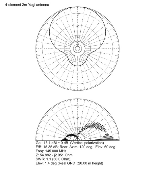
4-Element Yagi antenna for the 2m band
This blog post discusses the engineering design, construction, and performance evaluation of a 4-element Yagi-Uda antenna specifically optimized for the 2-meter amateur radio band, focusing on the frequency range of 144MHz to 145.5MHz. The project was initiated to establish strong and reliable communication with distant VHF repeaters of the RSSL (Radio Society of Sri Lanka), which are located approximately 58km and 96km from my location.

The primary objective was to develop a high-gain, directional antenna with a superior front-to-back ratio. This directionality is essential for maximizing signal capture from the desired repeater while minimizing interference and noise from unwanted directions, ultimately improving the SNR and the quality of the communication link.
VHF communication at these distances typically relies on line-of-sight propagation, making antenna gain a critical factor in overcoming path loss and achieving reliable signal levels.

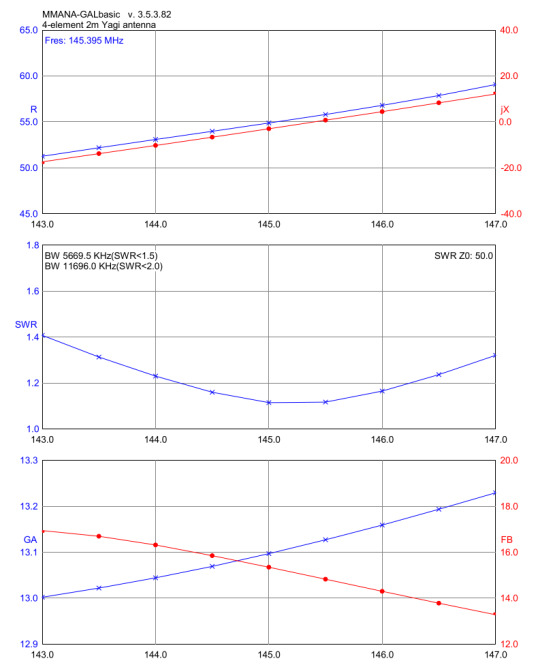
The antenna design was carried out using MMANA-GAL, a well-known and validated software suite based on the Method of Moments (MoM) for antenna analysis. While MoM simulations require significant computational resources, they deliver accurate predictions of antenna performance. This is achieved by breaking down the antenna structure into small segments and solving Maxwell's equations to determine the current distribution. This approach enables precise modeling of antenna impedance, radiation patterns, gain, and front-to-back ratio.
Key design parameters were iteratively optimized within MMANA-GAL to achieve the desired performance:
Target Frequency Band: 144MHz - 145.5MHz, encompassing the primary 2m amateur band frequencies.
Characteristic Impedance: 50Ω, to ensure impedance matching with standard RG-58 coaxial transmission line and transceiver equipment, minimizing reflected power and maximizing power transfer to the antenna.
Front-to-Back Ratio Optimization: Aiming for a high front-to-back ratio to minimize reception from the rear hemisphere, reducing interference and improving signal clarity, especially in noisy RF environments.
SWR Minimization: Achieving a VSWR as close to 1:1 as possible across the target frequency band. Low VSWR indicates efficient impedance matching and minimal power reflection back to the transmitter.
The simulation process involved adjusting the lengths of the elements and the spacing between them for the reflector, driven element, and directors of the Yagi antenna. This antenna operates on the principles of constructive and destructive interference of electromagnetic waves. The reflector, positioned behind the driven element, reflects waves forward, while the directors, located in front of the driven element, help to focus the radiated energy toward the main lobe. This arrangement increases both the forward gain and directivity of the antenna.

The optimized design, after multiple simulation iterations in MMANA-GAL, predicted the following performance metrics:
Simulated Gain: 13.1dBi. This represents a significant gain increase over a dipole antenna (approximately 2.15dBi) and translates to a substantial improvement in signal strength.
Simulated Front-to-Back Ratio: 15.35dB. This indicates that the power radiated in the forward direction is over 15dB stronger than in the backward direction, providing good directivity and rejection of rearward signals.
Simulated Input Impedance: Close to 50Ω across the 144MHz - 145.5 MHz band, ensuring a good match to standard 50Ω transmission lines.
The construction of the antenna focused on durability, lightweight design, weather resistance, and good electrical conductivity, all while keeping costs reasonable. We used 10mm diameter aluminum alloy tubes sourced from Lanka Aluminum. This diameter was selected because it is commonly available at many aluminum stores.
For the boom, we use a rigid 19.05mm (3/4 inch) square aluminum box bar, also sourced from Lanka Aluminum. This material is made from a similar aluminum alloy to ensure structural integrity and to serve as a common ground plane for the parasitic elements. The square profile enhances torsional stiffness compared to a round boom.
To effectively secure the components, we use 10mm ABS element holders. These holders are commonly utilized here to construct VHF/UHF TV antennas. Both the plastic holders and 10mm end caps are sourced from Kumarasinghe Radio.

The Polychrome junction box, measuring 85×85×50 mm and designed for outdoor use, is waterproof with an IP55 rating. This rating indicates that the box provides protection against dust ingress (although some dust may enter, it won’t cause harm) and shields against water jets from any direction. This makes it an essential choice for long-term outdoor deployment, ensuring the critical dipole feedpoint remains protected.
We used corrosion-resistant M3 stainless steel nuts, bolts, and washers to secure all elements and the IP box.
Precise assembly is crucial for achieving the intended performance of a Yagi antenna. All elements, except for the driven dipole, were directly and electrically bonded to the aluminum boom. This is a standard practice for Yagi antennas, as it utilizes the boom as a common ground, simplifying construction. Electrical connections were established using M3 stainless steel bolts that passed through pre-drilled holes in the aluminum tubes and boom, ensuring reliable electrical contact. The element holders provided mechanical support and maintained precise spacing between the elements, as well as a 90° angle with the boom, in accordance with the design specifications from MMANA-GAL.

The IP55 box containing the dipole was securely mounted to the underside of the aluminum boom using M3 stainless steel fasteners. To ensure consistent height with other elements, we used a strip of 10mm acrylic sheet.
Antenna VSWR and input impedance were measured across the frequency range of 144MHz - 145.5MHz using a VNA. The measured SWR of 1.1 at 145.025MHz confirms excellent impedance matching at the desired operating frequency. A Smith chart, generated by the VNA, visually represented the antenna's impedance characteristics throughout the band. It demonstrated that the impedance remained close to the target of 50Ω, indicating a broadband match across the intended operating frequencies.

The antenna was deployed at the designated operating location and oriented towards the target RSSL VHF repeaters. A subjective performance evaluation was conducted by attempting communication with the repeaters at distances of 58km (Yatiyanthota) and 96km (Piduruthalagala).
Reports from repeater users consistently indicated an S9+ signal strength, showing a significant improvement in reception when compared to a baseline mobile whip antenna.
You can find the complete design of this antenna, including all dimensions, in the PDF linked here. The Fusion 360 design file for the antenna is also available here. Additionally, the MMANA-GAL design file (in .mma format) can be downloaded from this link.
0 notes
Text
RDA5807M FM stereo receiver module
This project focuses on a simple yet powerful FM stereo tuner module. The core component of the module is RDA5807M, a single-chip broadcast FM stereo tuner that has gained popularity among designers in recent years due to its high level of integration. This integration significantly reduces the need for external components, simplifying circuit design. The RDA5807M supports a wide FM band, covering frequencies from 50MHz to 115MHz, making it adaptable to global FM standards.
Additionally, its use of a low-IF digital architecture streamlines the design process by requiring fewer external parts. The inclusion of an AGC (automatic gain control) feature ensures consistent signal reception, even in environments with fluctuating signal strengths.

The chip's digital stereo decoding capabilities deliver high-quality audio output, providing a rich stereo sound experience. Moreover, the energy efficiency of the RDA5807M makes it suitable for portable, battery-powered devices. The I2C control interface allows for easy integration with microcontrollers, enabling straightforward digital control.
This module is designed as a ready-to-use FM receiver solution, emphasizing compactness and ease of integration. It incorporates the RDA5807M IC and the STM8S003F3P MCU, along with the necessary supporting passive components, standard headers for connections, and flexible antenna connectivity options. The module is engineered to connect with commonly available 0.56-inch, 4-digit common cathode LED seven-segment display modules without any soldering.

The compact footprint of the module makes it ideal for projects where space is at a premium. Importantly, its open-source design allows for complete customization and modification.
It provides standard stereo audio output with separate left and right channels. The antenna input options allow for various antenna types, ensuring optimal signal reception. During testing, we utilized a 30cm long wire as the antenna and successfully received all FM stations clearly.
youtube
The tuner module features push switches to perform automatic station scans in both directions. The firmware limits the tuning range of the module to between 87MHz and 108MHz. Additionally, it includes digital volume control with 15 levels and a memory manager for storing up to 10 FM radio stations. The current tuner frequency is displayed on the segment display module, and there are two LEDs to indicate stereo reception and memory manager status.
The output level of this receiver module is not sufficient to drive speakers directly. Therefore, to achieve audio output through speakers, this module needs to be paired with a stereo audio amplifier. During testing, we successfully used the commonly available PAM8403 3W class-D audio amplifier with this module.

Power is supplied via a screw terminal, typically requiring a DC power source between 5V and 9V. The dimensions of the module are 72.85mm × 32.0mm.
This project is available on GitHub, providing schematics, PCB files, firmware source code, and comprehensive documentation. The hardware design of this project is licensed under CERN-OHL-W, while the firmware is licensed under the terms and conditions of the MIT license. All other resources, including documentation, are released under the Creative Commons Attribution 4.0 International license.
0 notes
Text
Resolving Keyboard Issues on the Sony ICF-SW7600GR
The Sony ICF-SW7600GR, a well-known portable shortwave receiver, has built a solid reputation for its performance and reliability. I purchased this receiver 20 years ago, and it is likely the last portable shortwave receiver manufactured by Sony. I primarily use it for shortwave listening, and it has functioned continuously for two decades. However, like all electronic devices, it is subject to component degradation over time. This post outlines the diagnostic and restorative procedures I undertook to address a complete failure of the keypad on this radio.

Initially, the radio exhibited a gradual decline in keypad functionality, which eventually led to a complete lack of response. I observed intermittent key input before all keypad operations ceased entirely. This symptom suggested a possible discontinuity or short circuit within the keypad interface circuitry.
To investigate further, I disassembled the unit to inspect the internal components. My primary focus was the flexible flat cable (FFC) connecting the front control panel to the main circuit board. A visual inspection revealed significant damage to the FFC. Specifically, the protective dielectric film had delaminated from the conductive traces, leading to potential short circuits between adjacent conductors. The FFC in question is an 18-pin cable with a forward direction, a 1.25mm pitch, and a length of 37mm.

Finding a replacement FFC with these specifications was challenging, both in local markets and popular online electronic component stores. Eventually, I consulted with a manufacturer called Shenzhen Yiwei Technology and was able to obtain a nearly identical cable. The only difference was that the new cable is 100mm long. Since this cable is located closer to the speaker, I carefully bent it and positioned it underneath the speaker magnet. Now, this cable is also available for purchase directly from the AliExpress store of the above mentioned manufacturer.

After replacing the FFC, I reassembled the unit and conducted tests. I was pleased to find that the keypad had fully restored functionality, with all keys responding as designed.

Compared to modern electronic repairs, this repair was quite straightforward. Thanks to its modular design, I was able to complete the repair using just a few Phillips screwdrivers and tweezers.
0 notes
Text
Analog pink noise generator
Pink noise is an essential tool in audio testing, widely used for analyzing speaker systems, room acoustics, and crossover networks. Unlike white noise, which has equal energy across all frequencies, pink noise features equal energy per octave, making it ideal for audio response testing. This characteristic ensures that pink noise offers a flat frequency response when analyzed on a logarithmic scale, providing a more accurate representation of audio systems.

We developed a this pink noise generator to meet various audio testing requirements. This device combines simplicity and performance, featuring a minimal component count for ease of assembly without compromising accuracy and usability. This pink noise generator design uses a reverse-biased emitter-base junction of a 2SC945 transistor as the noise source. In this configuration, the transistor behaves like a noisy zener diode, producing a broad spectrum of white noise.
In this design the NJM4558 op-amp is used to amplify and buffer the generated noise, ensuring high input impedance, stability, and consistent performance. At this stage above generated white noise is converted into pink noise using a 3dB/octave filter, which ensures equal energy distribution per octave over the audio frequency range.
The unit operates on a single-rail DC power source, compatible with 12V to 18V inputs. At our testing we found that this kit with 2SC945 from Matsushita electric starts to generate output at 8.4V and above. As we noticed this behavior is changing from vendor to vendor. For example some 2SC945's (It's manufacturer is difficult to identify) produces output at 9.1V. By considering most of the datasheets we decided 12V as the safest voltage which guaranteed the output.

To evaluate the performance of the pink noise generator, we paired it with the Simtelic KT0001 (LM386 power amplifier) module. This setup ensured that the output noise was sufficiently amplified for practical testing scenarios. This kind of setup is useful to identifying anomalies in speakers and crossover networks, measuring and optimizing room responses for audio clarity, and for microphone calibrations. When connecting this kit to an amplifier, pre-amplifier, or other analog audio equipment, always use shielded audio cables (UL1185 or equivalent) with the shortest possible length. Long, unshielded cables may introduce hum, oscillations, and distortion in the output.
The PCB for this module was fabricated by PCBWay, who generously sponsored this project. PCBWay offers high-quality PCB manufacturing and assembling services. Also, they offer CNC and 3D printing services. The pink noise generator PCB is available to order from PCBWay. Check out the PCBWay website for its manufacturing capabilities and pricing.
This kit is also available for purchase from Simtelic as a DIY kit. It is designed with through-hole components and can be assembled and tested without the need for specialized electronic assembly tools or instruments. For more details, refer to the kit's user manual provided on the Simtelic website.
0 notes
Text
Programmable Music Module
Simtelic Music Module is a user-programmable module that uses RTTTL data to store and play melodies.

RTTTL, which stands for Ring Tone Text Transfer Language, was created to provide a simple, text-based format for sharing ringtones on early mobile phones. Developed by Nokia, it quickly became popular due to its compact size and compatibility with text messaging services. This format allowed users to easily exchange custom melodies without needing specialized software or data connections.
RTTTL is a human-readable data format where each ringtone is represented as a sequence of notes, durations, and optional settings.
According to Simtelic naming conventions, this module is identified as EL0003 and is available for purchase online.

This module is built around a 32-bit MCU, a 2Kbit EEPROM, and a CH340 USB bus conversion chip. It is compatible with the latest Windows and Linux-based PCs. The module is user-friendly and provides capabilities similar to the older UM series musical chips. Its main objective is to serve as a replacement for popular melody generator chips such as the UM66, UM3561, UM3481, and others.
This module is powered by the USB bus and provides an analog AF output. It is capable of driving a small 8Ω speaker. The module features a jumper to select between different playback modes. When the jumper is open, it plays a programmed melody on a continuous loop. When the jumper is closed, the melody plays only once. To play the melody again, the user must press the push button on the module.
youtube
To flash the module, use the RTTTL loader script available in the Simtelic GitHub repository. This Python script connects to the module and transfers the specified RTTTL data file into it. The programming process takes less than 20 seconds and automatically resets the module after the flashing operation is complete. With this script, users can upload RTTTL data into the module, which can be up to 256 characters long.
RTTTL models can easily be found on the web. A few notable repositories are FlipperMusicRTTTL and the RTTTL player. Note that all RTTTL scripts provided on these sites do not work with this module, as it can only accommodate melodies that are up to 256 characters long.
This module has certain limitations. It primarily supports monophonic melodies and provides limited control over complex musical elements such as rests, ties, or dynamic changes. These limitations are inherent to RTTTL.
The module datasheet is available on the Simtelic product page.
0 notes
Text
Adapting HX711 modules for 3.3V Operation
The HX711 is a versatile integrated circuit (IC) designed for precision analog-to-digital (A/D) conversion, particularly suited for strain gauge load cell applications. It features a 24-bit A/D converter with a differential input stage capable of handling both single-ended and differential input signals. Additionally, this device offers adjustable gain amplification to accommodate various load cell sensitivities.

A common module based on the HX711 available in the market, including on AliExpress, is shown below. This module utilizes its internal analog supply regulator, which ensures a stable analog supply (AVDD) for the ADC and other internal components. The output voltage of the regulator (AVDD) is calculated using the following formula: VAVDD = VBG × (R1 + R2) / R2.

According to the electrical characteristics listed in the datasheet, the reference bypass voltage (VBG) is 1.25V. For the modules mentioned, R1 is set at 8.2kΩ and R2 at 20kΩ. By substituting these values into the formula, we calculate AVDD to be approximately 4.29V.

The HX711 IC operates within a voltage range of 2.6V to 5.5V. However, many HX711 modules on the market come with an internal voltage regulator that outputs approximately 4.29V. This can pose challenges when using the module with 3.3V microcontrollers. Furthermore, the datasheet specifies that the output voltage of the regulator should be at least 100mV lower than the supply voltage (VSUP), making the current regulator's output voltage incompatible with 3.3V supply voltages.

To address this, we need to ensure that AVDD is within the 2.6V to 3.2V range to make the module compatible with both 3.3V and 5V systems. After conducting some calculations, we determined that replacing R1 with 10kΩ and R2 with either 15kΩ or 12kΩ would be ideal. Using a 15kΩ resistor gives an AVDD of 3.1V, while using a 12kΩ resistor reduces it to 2.75V. In one of our experimental boards, we opted to replace R2 with a 12kΩ resistor.

As a further test, we lowered the AVDD to approximately 1.6V, and at this voltage, the HX711 still produced the correct results in our test setup. Interestingly, we observed that swapping R1 and R2 allows us to achieve an AVDD of 1.76V. To test this, we swapped R1 (8.2kΩ) and R2 (20kΩ) in one of the modules, and after applying a 5V supply, we noted that the AVDD returned at 1.65V, with the HX711 still providing correct outputs.

To evaluate the boards, we created a quick prototype using the STM32F405 MCU. In this prototype, we powered the HX711 module with 3.3V and directly connected its I/O pins to the STM32 GPIO pins.
For interaction with the module, we utilized the HX711 library provided at https://github.com/PCov3r/HX711-STM32-Library. The source code for our test firmware is available here.
After making the above modifications, all modules produce a stable output at 3.3V. We tested these modules with both 3.3V and 5V MCUs, using 5kg, 10kg, and 20kg load cells, and it operated correctly across all these combinations.
0 notes
Text
Alarm unit for limit switches or flow switches
Have you ever faced the frustration of dealing with an overflowing tank or a pump running dry? These unexpected events can result in costly damage and inconvenience. A reliable floater switch alarm system can provide early warnings, allowing you to take prompt action and prevent further issues. This project guides you through building a do-it-yourself floater switch alarm system using a PIC12F508 microcontroller.

The circuit for this project is relatively simple and requires very few components. The system is designed to operate with a 12V DC power supply and utilizes a 230V AC buzzer unit for audible alerts.
The circuit includes a mute function that allows you to temporarily silence the alarm for a specified duration. Additionally, a built-in timeout mechanism ensures continuous alarm activation if the floater switch remains closed for an extended period, indicating a potential emergency. This project is suitable for various applications, including home or industrial monitoring, and environmental monitoring.
The firmware for the microcontroller will control the operation of the alarm system. It should perform the following tasks:
Monitor the floater switch: Continuously read the input pin from the floater switch.
Activate the alarm: If the floater switch detects a change in water level (e.g., rising water), activate the buzzer or alarm.
Mute function: Allow the user to temporarily mute the alarm by pressing a button.
Timeouts: If the alarm remains active for an extended period, it may indicate a serious issue.
The firmware for this project is developed using the MPLAB X IDE and the XC8 C compiler. The latest firmware source code is available in the firmware directory of the project repository. The compiled firmware is also available in the release section of the project repository.

To protect the electronic components from moisture and other environmental factors, it is recommended to enclose the system in a waterproof enclosure. In our prototype build, we use an 100mm × 68mm × 50mm project enclosure to mount this controller.
This is an open hardware project. All the project firmware source code, design files, and compiled binaries are available on the GitHub project page.
0 notes
Text
RDS Data Extraction with RFtap and Wireshark
RDS (Radio Data System) is a communication protocol standard used for embedding small amounts of digital information in traditional FM radio broadcasts. It enables radio stations to transmit data such as station identification, program information, and traffic updates.
To capture and decode RDS data, one method involves using a Software Defined Radio (SDR) along with GNU Radio and RFtap. GNU Radio provides a framework for creating software radios, while RFtap acts as a bridge between GNU Radio and conventional network monitoring and packet analysis tools like Wireshark.

Unfortunately, as of the time of writing, RFtap is no longer being maintained and does not work with the latest version of GNU Radio (version 3.10.10). This post offers guidelines for rebuild and using RFtap with the new GNU Radio release.
This post assumes that the reader has access to DVB-T dongles based on the Realtek RTL2832U and a PC running Ubuntu or Debian Linux. For this, I used an RTL dongle with Rafael Micro R820T tuner and Ubuntu 24.04 LTS release.
As the first step install the following GNU Radio build dependencies into the OS:
sudo apt-get install cmake libboost-all-dev \ liblog4cpp5-dev qtcreator qtbase5-dev \ qt5-qmake python3-cheetah python3-numpy \ python3-pygtk python3-gi python3-gi-cairo \ gir1.2-gtk-4.0
sudo apt install git g++ libgmp-dev swig \ python3-mako python3-sphinx python3-lxml \ doxygen libfftw3-dev libsdl1.2-dev \ libgsl-dev libqwt-qt5-dev libqt5opengl5-dev \ python3-pyqt5 liblog4cpp5-dev libzmq3-dev \ python3-yaml python3-click \ python3-click-plugins python3-zmq python3-scipy \ libcodec2-dev libgsm1-dev libusb-1.0-0 \ libusb-1.0-0-dev libudev-dev \ python3-setuptools
sudo apt install pybind11-dev python3-matplotlib \ libsndfile1-dev libsoapysdr-dev soapysdr-tools \ python3-pygccxml python3-pyqtgraph
sudo apt install libiio-dev libad9361-dev \ libspdlog-dev python3-packaging python3-jsonschema \ python3-qtpy
sudo apt remove swig
Next, clone and build Volk (Vector-Optimized Library of Kernels)
mkdir ~/rf cd rf git clone --recursive https://github.com/gnuradio/volk.git cd volk mkdir build cd build cmake -DCMAKE_BUILD_TYPE=Release -DPYTHON_EXECUTABLE=/usr/bin/python3 ../ make sudo make install sudo ldconfig
After installing the Volk library, we can proceed to build GNU Radio.
cd ~/rf wget https://github.com/gnuradio/gnuradio/archive/refs/tags/v3.10.10.0.tar.gz tar -xvf ./v3.10.10.0.tar.gz cd gnuradio-3.10.10.0 mkdir build cd build cmake -DCMAKE_BUILD_TYPE=Release -DPYTHON_EXECUTABLE=/usr/bin/python3 ../ make -j8 make test sudo make install sudo ldconfig

Now GNU Radio is installed with all necessary components. To enable RTL SDR support, we must build and install Osmocom RTL SDR libraries and SDR components.
cd ~/rf git clone https://gitea.osmocom.org/sdr/rtl-sdr.git cd rtl-sdr mkdir build cd build cmake ../ -DINSTALL_UDEV_RULES=ON make sudo make install sudo ldconfig
cd ~/rf git clone https://gitea.osmocom.org/sdr/gr-osmosdr cd gr-osmosdr mkdir build cd build cmake ../ make sudo make install sudo ldconfig
Before plugging in the RTL-SDR dongle, we need to prevent the kernel modules for the RTL-SDR USB device from being loaded into the kernel and taking ownership of the device. To do this, simply navigate to the /etc/modprobe.d directory and create a file called rtl-sdr-blacklist.conf with the following content:
# This system has librtlsdr0 installed in order to # use digital video broadcast receivers as generic # software defined radios. blacklist dvb_usb_rtl28xxu blacklist e4000 blacklist rtl2832 blacklist rtl2830 blacklist rtl2838
Next, you should clone and build the FM RDS/TMC transceiver module for GNU Radio.
cd ~/rf wget https://github.com/bastibl/gr-rds/archive/refs/tags/v3.10.tar.gz tar -xvf ./gr-rds\ -v3.10.tar.gz cd gr-rds-3.10 mkdir build cd build cmake .. make sudo make install sudo ldconfig
For the next steps, we need to have Wireshark and RFTap. Wireshark can be installed using a package manager.
sudo apt-get install wireshark
To run Wireshark without requiring root user permissions, use the following set of commands:
sudo dpkg-reconfigure wireshark-common sudo usermod -a -G wireshark $USER newgrp wireshark
A message may be prompted in the first step above and proceed by selecting the "Yes" option.
Now restart the OS and continue with the RFTap installation.
The official RFTap repository is no longer being maintained and is not compatible with newer versions of GNU Radio. For this step, please use the RFTap fork available in my GitHub repository. This version has been successfully tested with GNU Radio 3.10.10 and Wireshark 4.2.2.
cd ~/rf git clone https://github.com/dilshan/gr-rftap.git cd gr-rftap mkdir build cd build cmake .. make sudo make install sudo ldconfig
Now get the modifier version of rds_rx_rftap.grc from the above repository.

The Wireshark Dissector file for RDS data is also available in the repository. Copy it to the ~/.config/wireshark/plugins directory. Create the directories if they do not exist.
Launch Wireshark and monitor the loopback (lo) adapter. Start GNU Radio and execute the rds_rx.grc file, which was downloaded in the above step.
youtube
If all the steps are performed correctly, the RDS data should appear in the packet list pane as UDP messages. The dissected messages can be observed through the packet bytes pane.
0 notes
Text
Echo Generator for Microphones
This project is about a single-channel microphone echo generator circuit. This circuit builds around the Holtek HT8970 echo effect generator IC. It offers complete control of the echo effect by providing delay, mix, and output level adjustments.

HT8970 is an echo/surround sound effect generator IC with 20Kb SRAM. It also contains the built-in VCO stage, AD, and DA converters. The chip costs less than 0.5 US$ and is commonly available in the market.
The given schematic offers a maximum of 320ms time delay and works with a single-rail 9V DC power supply.
In addition to the HT8970 integrated circuit, this circuit uses an NJM4558 op-amp to amplify the input and output audio signals. HT7150 voltage regulator uses in this design to power up the HT8970 IC. The HT7150 is a low-power 5V regulator IC from Holtek, the same maker of the HT8970 IC.
The circuit designs to work with 500Ω dynamic microphones. For microphone connectivity, this circuit provides a standard XLR connector. The output audio signal of this echo generator can directly couple to an AF power amplifier or a PC sound card.
youtube
We successfully tested this circuit with the EC042 dynamic microphone at the testing stages. To power up this circuit, we use a 9V DC power supply. As we observed, the maximum current drawn by this circuit was around 50mA during our test phase.
The PCBWay sponsored this project. PCBWay offers high-quality PCB manufacturing and assembling services. Also, they offer CNC and 3D printing services. The PCB of the echo effect generator is available to order from PCBWay. Check out the PCBWay website for its manufacturing capabilities and pricing.

The PCB design of this circuit uses only through-hole-type components. The dimensions of the PCB are 84.5mm × 71.0mm.
All the schematic, KiCAD PCB design files, and BoM of this circuit is available to download at this google drive location.
Overall this echo effect generator provides a natural echo sound effect. The only drawback we noticed with this IC is the significant distortion in the sound at the peak delay point.
0 notes
Text
Universal HD44780 LCD interface
YALI (Yet Another LCD Interface) is an open-source project to provide a universal interface to drive the popular Hitachi HD44780 LCD controller. This module supports 3.3V and 5V MCUs and hardware development platforms, including Arduino, STM32, PIC, and ESP8266.

The hardware module of this project consists of a 74HCT08 CMOS AND gate and a 74HC595 8-bit serial-in, parallel-out shift register. This module uses the MP1540 step-up converter to power the LCD unit connected to the system. The module has the jumper to select 3.3V or 5V DC power input.

The YALI library is developed using C and is designed to be easily integrated with any C/C++ embedded toolchain. At the initial design stages, this library was successfully tested with all Arduino development boards, NodeMCU, STM32 Blue Pill, etc. The target system must have three digital output lines with 5V or 3.3V logic levels to interface with the YALI module. As mentioned earlier, this module works successfully with 5V or 3.3V power sources and logic levels.
The YALI library provides a unified API to control the HD44780 LCD controller. It has functions to handle cursor control, custom character loading, LCD backlight control, etc.
youtube
The PCBWay sponsored this project. PCBWay offers high-quality PCB manufacturing and assembling services. Also, they offer CNC and 3D printing services. The PCB of the YALI module is available to order from PCBWay. Check out the PCBWay website for its manufacturing capabilities and pricing.
The dimensions of the YALI hardware module are 69mm × 21mm. This module is designed using SMD components and can be connected directly to the LCD unit.

This project is an open-source hardware project. All its design files, BOM, schematics, and firmware source codes are available at Github.com.
The PCB design, schematic, and other design files of this project are covered with a Attribution-ShareAlike 4.0 International license. The library source code is released under the terms of the MIT license.
#LCD#HD44780#display#PIC#Arduino#MPLAB#XC8#STM32#ESP8266#LibOpenCM3#74HC595#74HTC08#MP1540#module#API#FreeRTOS#NodeMCU#Youtube
1 note
·
View note
Text
6-channel speaker selector
At the beginning of 2018, we developed the first version of the 6-channel speaker selector using PIC16F88 MCU and ULN2803 Darlington transistor array. In this new design, we redesign it with low-cost MCU and Darlington transistor arrays. This design also provides the same functionality as the 6-channel speaker selector switch we designed earlier.
This new speaker selector uses STC15W201 MCU. This MCU is a low-cost 8051 MCU designed by STC micro. At the time of this writing, the STC15W201 can obtain for less than US$ 0.8. To drive the seven segments and to control the relays, this design uses the popular 74HC595 8-bit shift register ICs.

To select each speaker channel, we use pair of 12V DPDT relays. These relays interface to 74HC595 through a ULN2001D 3-channel Darlington transistor array IC. This 3-channel Darlington driver IC is functionally equivalent to the famous 8-channel ULN2003 IC. This ULN2001D version is an 8-pin IC and is available in both DIP-8 and SOP-8 packages.
This new board is designed to work with a 12V DC power supply and in our prototype build, we use a 12V/5A SMPS unit to power the whole system.
To get the optimal results with this circuit, use an Omron G2R-2-12DC or an equivalent type of relay with a coil current lower than 100mA.
The firmware of the STC15W201S is developed using SDCC. To flash the MCU, we use stcgal. Thanks to the built-in bootloader, we can program this MCU using a generally available 5V USB to UART module/dongle.
The complete build process of the speaker selector is shown in the video below:
youtube
The functionality of the firmware is almost identical to the old PIC16F88 firmware. After powering up the system, the active speaker channel is displayed on the seven-segment display. To switch to a different speaker channel, press the button repeatedly with short intervals.
To mute or disconnect the current speaker channel, press and hold the same button for more than 3 seconds.
As described above, all functions of this circuit can be the control using a single push switch.

The PCBWay sponsored this project. PCBWay offers high-quality PCB manufacturing and assembling services. Also, they offer CNC and 3D printing services. The Speaker selector PCB is available to order from PCBWay. Check out the PCBWay website for its manufacturing capabilities and pricing.
This project is an open-source hardware project. All its design files, schematics, and firmware source codes are available at Github.com.
The PCB design, schematic, and other design files of this project are covered with a CERN-OHL-W 2.0 license. Firmware source code is released under the terms of the MIT license.
#audio#8051#STC15W201#ULN2001D#74HC595#switch#speaker-selector#electronic-switch#AMS1117-5.0#PCBWay#prototype#SDCC#Relay#STC#Youtube
0 notes
Text
5.1 channel analog audio processor
In this project, we developed a 5.1-channel analog audio processor using PT2322 IC. PT2322 is an inexpensive analog audio processor introduced by Princeton Technology Corporation. It contains 6-channel individual channel attenuators, a 3-way tone control system for front-end speakers, and a 3D audio simulation system.

In this design, we combine PT2322 with Arduino Nano and interface it with PC/embedded computing boards through a USB port. Native GTK UI application provides to control all functions of the PT2322 IC.
The Arduino Nano can directly plugin to the PT2322 module. There are three push buttons on the panel itself to control the volume and mute the audio.
To reduce the cost and minimize the PCB size, we use both SMD and through-hole-type components in this PCB. The dimension of the PCB is 59mm × 60mm. The PCB of this module can directly order from the PCBWay project page. Using the PCBWay service, you can order high-quality PCBs at low prices. Use the PCBWay online quote tool for pricing and more details.

The Arduino firmware in this project is developed using PlatformIO. The host-side control application is written using GCC C. This UI application can be compiled and run on any Linux/GTK compatible board like PCs, Raspberry Pi, Orange Pi, BeagleBone Black, etc. All communication between the host and the module is performed through the USB UART interface provided by the Arduino Nano board.

At the prototyping stage, we test this board using an ASUS Xonar SE 5.1 channel soundcard and Creative Inspire T6300 - 5.1 analog speaker system. The above setup delivers clean audio output without any noticeable distortion.
In PT2322, the tone control system applies to front-end channels only. The remaining channels work independently from the tone control system. This is a design limitation of the IC. From our experience, this can sometimes adversely affect the surrounding listening experience.
The PT2322 has a 3-way tone control system that allows bass, mid-range, and treble control over a range of -14dB to +14dB. A 6-channel attenuation system provides up to 15dB attenuation per channel. All these controls divide into 15 steps. The master volume control can use to adjust attenuation from 79dB to 0dB in 80 steps.

This audio processing module is an open-source hardware project. All the design files, source codes, and compiled binaries are in the project repository at github.com.
#2N7002#PT2322#Arduino#Arduino Nano#Audio#USB#Linux#GTK#Surround#raspberry pi#orange pi#banana pi#BeagleBone Black#platformIO#I2C#LM78M08#UART#serial#gcc
0 notes
Text
Virtual electronic finderscope for the Stellarium
StarPointer is a virtual electronic finderscope for astronomical telescopes. This device works with Stellarium and helps the observer identify objects in the sky.
This unit can be attached to the telescope without modifications and connects with the computer through the USB port. The StarPointer uses a few onboard sensors to determine its angle and position. After obtaining that information, the unit calculates the RA (right ascension ) and DEC (declination) coordinates of the telescope and transfers those details to the Stellarium.
The StarPointer builds around the STM32F103C8 microcontroller, ADXL345 3-axis accelerometer, and HMC5883L 3-axis magnetometer. This unit communicates with the PC using the inbuilt USB peripheral of the STM32F103C8 microcontroller. The firmware of the StarPointer is developed using the LibOpenCM3 library and built using GNU ARM Embedded Toolchain.
youtube
This unit can attach to any astronomical telescope or binocular regardless of its type or mount. After attaching the unit, the user needs to calibrate the StarPointer using the configuration software. This configuration software allows StarPointer to set the latitude and longitude of the observation location, RTC date/time, and RA and DEC offsets. After performing the above steps, the unit is ready to use with the Stellarium.
The StarPointer is designed to work with Stellarium's telescope control plugin. Its firmware has been developed to work with the Meade LX200 communication protocol, and no additional modifications are needed for Stellarium to work with this sensor kit.
When assembling the sensor module, we strongly recommended using the genuine STM32F103C8T6 MCU for this project. During the prototyping stages, we found a few counterfeit STM32F103C8T6 MCUs which are not working properly with this firmware. According to our observations, most of the counterfeit STM32F103C8T6 MCUs failed to initialize the RTC and USB peripherals at the startup.
We also design a suitable enclosure for this project, and its design files are available to download at tinkercad.com. This design can be 3D printed using either ABS or PLA. To get the optimal results, we recommended attaching this enclosure to the piggyback bracket of the telescope.
The PCBWay sponsored this project. PCBWay offers high-quality PCB manufacturing and assembling services. Also, they offer CNC and 3D printing services. The StarPointer PCB is available to order from PCBWay. The StarPointer enclosure can also order from the PCBWay 3D printing service. Check out the PCBWay website for their manufacturing capabilities and pricing.

StarPointer is an open hardware project. All design files, firmware/application source codes, and schematic files are available to download at the project GitHub repository. The complete documentation is also available in the Wiki section of the GitHub repository.
#accelerometer#ADXL345#ARM#CDC#celestron#finderscope#gcc#HMC5883L#lazarus#LibOpenCM3#LX200#magnetometer#Meade#PCBWay#RT9193-33#Stellarium#STM32F103C8T6#telescope#USBLC6-2SC6#USB#RTC#Youtube
0 notes
Text
Experimental narrowband FM receiver for the 2-meter band
This project is about MC3362 and ADF4351 based modularized, 2-meter narrow band FM receiver. In this design, the receiver splits into three modules as RF preamplifier, MC3362 tuner, and ADF4351 oscillator. The RF preamplifier builts around BF900 dual-gate MOSFET. The tuner stage builts using the popular MC3362, low power narrowband FM receiver IC. For the oscillator, we use the ADF4351 DDS RF signal generator module.
The core component of this receiver is MC3362 IC. This IC was designed by Motorola and is no longer in production, but this IC is still available to purchase in many online stores. The chip we used in this receiver was purchased from a local electronic component store for LKR 75 (USD 0.2).
The RF preamplifier used in this receiver extracts from the N.Ganesan's (VU3GEK) LRR200, 2-meter band FM receiver project.

In this prototype, the above preamplifier was built as a module using a Manhattan construction technique. The SO-239 antenna input socket is also soldered directly to the preamplifier board. The preamplifier output connects to the input of the 1st mixer stage of MC3362 via a 50Ω coaxial link. This preamplifier is designed to operate using an 8V DC power source. If the BF900 transistor is not available, use an equivalent dual-gate, UHF range, N-channel MOSFET transistor.

The tuner stage of this receiver is a minimal version of the MC3362 circuit. This tuner module mainly consists of 10.7MHz and 455kHz ceramic filters, a 42IF301 - I.F transformer, and a 10.245MHz crystal. The local oscillator stage of this receiver is modified to use the ADF4351 RF signal generator. During the prototyping stages, we drive this module using a 5V DC power source.

For the oscillator stage, we use the ADF4351 DDS RF signal generator module. Apart from the ADF4351 signal generator, this module has an STM32F103-based driver and a TFT touch LCD. The RF output of this oscillator is directly connected to one of the local oscillator terminals of MC3362 IC. This module is designed to work with 5V. The supply voltage is feeding to the module through the onboard USB connector.
youtube
During the prototyping stages, we connect the AF output of this receiver to the TPA3001D1 power amplifier. Any AF power amplifier with 3W or higher rated output will work well with this receiver.
After connecting a suitable antenna, we were able to receive a very clear 2-meter band signal from the receiver. During the testing phase, we got extremely good reception of the RSSL VHF net at 145.625MHz (local oscillator frequency - 134.875MHz) from this receiver. For this test, we used a 5-element (homebrew) Yagi antenna.

PCBWay sponsored this project. PCBWay offers high-quality PCB manufacturing, PCB assembly, and CNC/3D printing services for a competitive price. Check their website for more information and pricing.
All the KiCAD design files and schematic diagrams are available on google drive.
#MC3362#BF900#ADF4351#VHF#Radio#RF#DDS#NFM#TPA3001D1#Tuner#ham radio#42IF301#amateur radio#LCD#Youtube
0 notes
Text
Wireless Call Bell
This project is about a wireless musical call bell, which I designed to meet some of my friend's requirements. This circuit design uses only the 4000 series CMOS logical ICs, NE555, UM66, and TDA7233 audio amplifier IC. For the remote control, we use a 433MHz 4-channel remote control module. This circuit is designed to work continuously with a low-power external 5V power supply.

The PCB in this call bell is designed as a single-sided PCB. The dimension of the PCB is 82mm × 50mm.
All the components in this circuit are commonly available through-hole-type components. The whole assembly process of this musical call bell is shown in the video attached to this document.
youtube
The RF remote control module we use in this project consists of a remote control decoder and encoding IC. In our version, the transmitter (key fob) has a PT2262 encoder, and the receiver has a PT2272 decoder IC. In the prototype build, the receiver and transmitter are configured to use the default address code. To utilize different address codes, tie appropriate address pin(s) to the VCC or GND on both transmitter and receiver.
To improve the working distance of the receiver, we attach a small helical antenna to the receiving module. This antenna is constructed using a 22 S.W.G telephone wire, and its dimensions are illustrated below:

With the antenna above, we successfully trigger the bell at a distance of 20 m through a few brick walls.
For the housing, we use a 196mm × 90mm × 60mm ABS project box. The drilling layout for the enclosure is illustrated below:

All the schematic, BOM, and PCB design files of this musical call bell are available from here.
#bell#CD4013#CD4072#CD4069#NE555#TDA7233#PT2262#PT2272#remote#4-channel#UHF#433MHz#antenna#helical#UM66#RF#2N3904#Youtube
0 notes
Text
Infrared remote control clone utility
IR Clone is an open-source IR remote control analyzer tool. This utility can analyze any IR remote control that modulates the IR signal with a 38kHz carrier signal. This utility has an option to store and retrieve up to 16 IR signals. In addition, it has PC software to analyze and edit captured IR signals.
The hardware component of this analyzer is built around the STM8S003F3 MCU. It has 24LC32 EEPROM installed to store the captured IR signals. This unit is designed to operate with a 5V to 9V DC power source or a 3V battery.

Operating modes such as capture or replay can be changed using an onboard jumper on the PCB. These operating modes can change at any time without restarting the unit.
In addition to the IR clone PCB, the only external component needed to operate this system is a 4×4 matrix keypad. Most of the generally available 4×4 keypads can directly couple with this system.
The dimensions of the IR Clone PCB are 41.2mm × 32.1mm, and it has been designed using both SMD and through-hole type components. In this given design, the TSOP1838 IR decoder has been used to capture the incoming signals. The output stage of this system consists of LD271, KCL5587S, or equivalent 880nm to 950nm (IR) LED. The 38kHz modulation signal required by the output stage is generated using built-in timers of the STM8S003 MCU.

Captured waveforms stored in the EEPROM can be decoded directly using the IR Clone software provided in the repository. Using this application, the user can visualize and edit the captured signals. Both IR clone software and hardware supports up to 16 channels.
To transfer the EEPROM data to the PC, use any 24LC family compatible EEPROM reader or programmer. In our presentations, we used an inexpensive CH341A based programmer to read and write the 24LC32 EEPROM.
youtube
In addition to the IR Clone software, the repository also contains a sample Python script that exhibits decoding of EEPROM data.
IR Clone is an open-source project. All the documentation, schematics, PCB design files, firmware source codes, and application source codes are available at the project repository at GitHub.com.
#24C32#IR#Infrared#STM8S003F3#SDCC#CH341A#ch341eeprom#clone#duplicator#EEPROM#ST-Link#TSOP1838#LD271#AMS1117-3.3#Analyzer#MMBT3904#stm8flash#waveforms#Youtube
0 notes